SIDECAR ASIC Control Electronics on a Chip June

- Slides: 21

SIDECAR ASIC Control Electronics on a Chip June 24 th 2005 Markus Loose

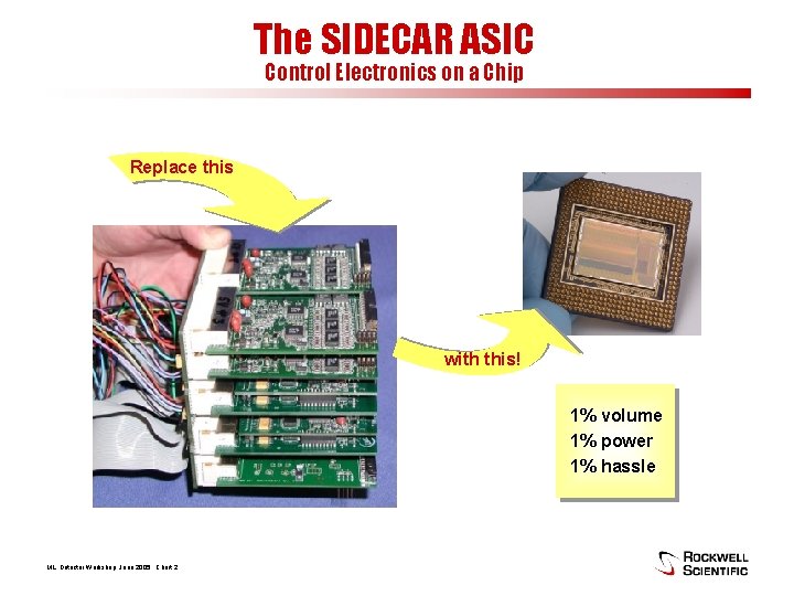
The SIDECAR ASIC Control Electronics on a Chip Replace this with this! 1% volume 1% power 1% hassle ML, Detector Workshop, June 2005 Chart 2

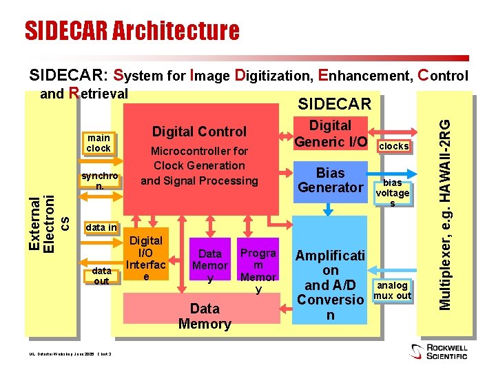
SIDECAR Architecture main clock External Electroni cs synchro n. Digital Control Microcontroller for Clock Generation and Signal Processing Digital Generic I/O Bias Generator clocks bias voltage s data in data out Digital I/O Interfac e Data Memor y Data Memory ML, Detector Workshop, June 2005 Chart 3 Progra m Memor y Amplificati on and A/D Conversio n analog mux out Multiplexer, e. g. HAWAII-2 RG SIDECAR: System for Image Digitization, Enhancement, Control and Retrieval SIDECAR

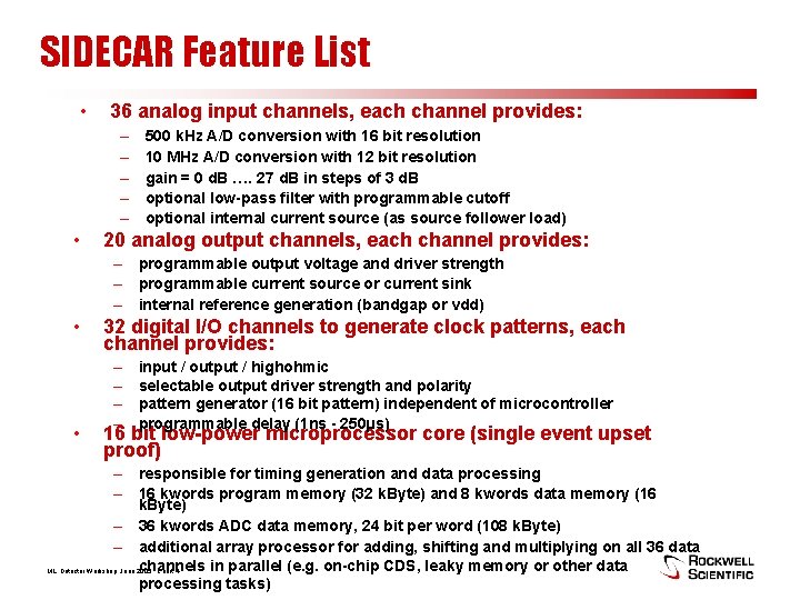
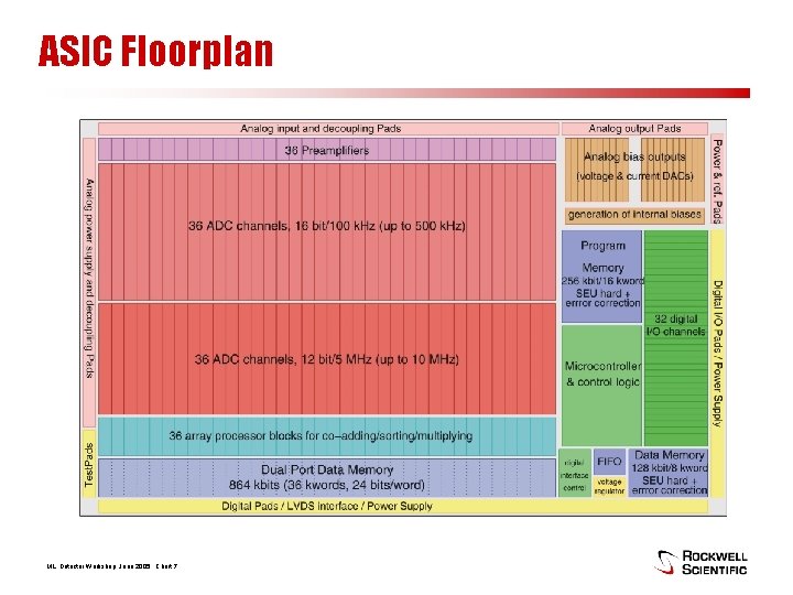
SIDECAR Feature List • 36 analog input channels, each channel provides: – – – • 500 k. Hz A/D conversion with 16 bit resolution 10 MHz A/D conversion with 12 bit resolution gain = 0 d. B …. 27 d. B in steps of 3 d. B optional low-pass filter with programmable cutoff optional internal current source (as source follower load) 20 analog output channels, each channel provides: – programmable output voltage and driver strength – programmable current source or current sink – internal reference generation (bandgap or vdd) • • 32 digital I/O channels to generate clock patterns, each channel provides: – – input / output / highohmic selectable output driver strength and polarity pattern generator (16 bit pattern) independent of microcontroller programmable delay (1 ns - 250µs) 16 bit low-power microprocessor core (single event upset proof) – responsible for timing generation and data processing – 16 kwords program memory (32 k. Byte) and 8 kwords data memory (16 k. Byte) – 36 kwords ADC data memory, 24 bit per word (108 k. Byte) – additional array processor for adding, shifting and multiplying on all 36 data channels in parallel (e. g. on-chip CDS, leaky memory or other data ML, Detector Workshop, June 2005 Chart 4 processing tasks)

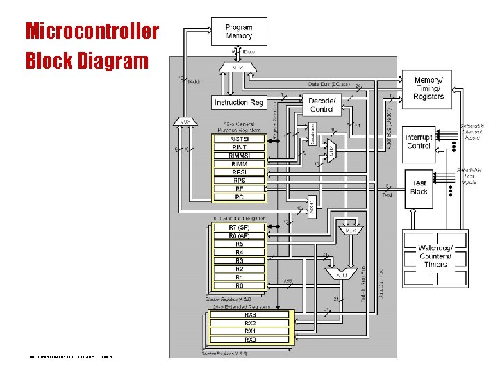
Microcontroller Block Diagram ML, Detector Workshop, June 2005 Chart 5

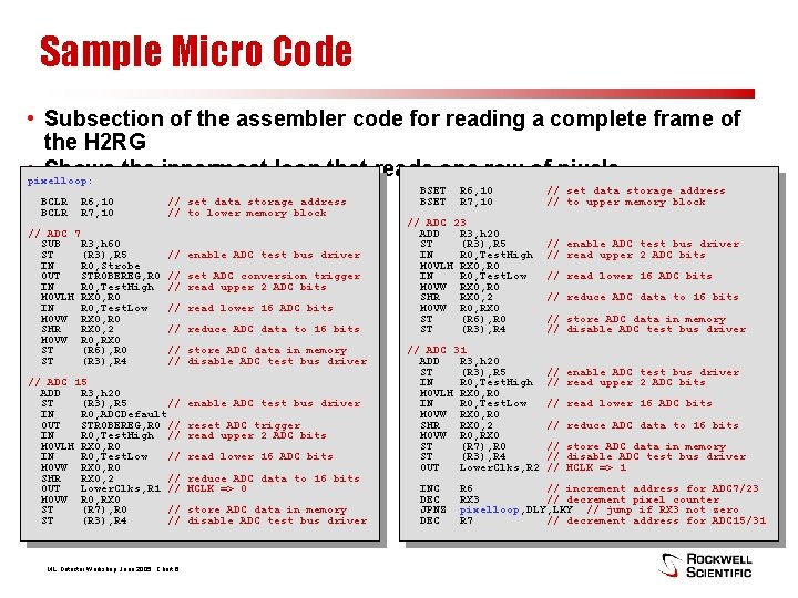
Sample Micro Code • Subsection of the assembler code for reading a complete frame of the H 2 RG • pixelloop: Shows the innermost loop that reads one row of pixels BCLR R 6, 10 R 7, 10 // ADC 7 SUB R 3, h 60 ST (R 3), R 5 IN R 0, Strobe OUT STROBEREG, R 0 IN R 0, Test. High MOVLH RX 0, R 0 IN R 0, Test. Low MOVW RX 0, R 0 SHR RX 0, 2 MOVW R 0, RX 0 ST (R 6), R 0 ST (R 3), R 4 // set data storage address // to lower memory block // enable ADC test bus driver // set ADC conversion trigger // read upper 2 ADC bits // read lower 16 ADC bits // reduce ADC data to 16 bits // store ADC data in memory // disable ADC test bus driver // ADC 15 ADD R 3, h 20 ST (R 3), R 5 // IN R 0, ADCDefault OUT STROBEREG, R 0 // IN R 0, Test. High // MOVLH RX 0, R 0 IN R 0, Test. Low // MOVW RX 0, R 0 SHR RX 0, 2 // OUT Lower. Clks, R 1 // MOVW R 0, RX 0 ST (R 7), R 0 // ST (R 3), R 4 // ML, Detector Workshop, June 2005 Chart 6 enable ADC test bus driver reset ADC trigger read upper 2 ADC bits read lower 16 ADC bits reduce ADC data to 16 bits HCLK => 0 store ADC data in memory disable ADC test bus driver BSET R 6, 10 R 7, 10 // ADC 23 ADD R 3, h 20 ST (R 3), R 5 IN R 0, Test. High MOVLH RX 0, R 0 IN R 0, Test. Low MOVW RX 0, R 0 SHR RX 0, 2 MOVW R 0, RX 0 ST (R 6), R 0 ST (R 3), R 4 // ADC 31 ADD R 3, h 20 ST (R 3), R 5 IN R 0, Test. High MOVLH RX 0, R 0 IN R 0, Test. Low MOVW RX 0, R 0 SHR RX 0, 2 MOVW R 0, RX 0 ST (R 7), R 0 ST (R 3), R 4 OUT Lower. Clks, R 2 INC DEC JPNZ DEC // set data storage address // to upper memory block // enable ADC test bus driver // read upper 2 ADC bits // read lower 16 ADC bits // reduce ADC data to 16 bits // store ADC data in memory // disable ADC test bus driver // HCLK => 1 R 6 // increment address for ADC 7/23 RX 3 // decrement pixel counter pixelloop, DLY, LKY // jump if RX 3 not zero R 7 // decrement address for ADC 15/31

ASIC Floorplan ML, Detector Workshop, June 2005 Chart 7

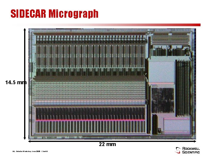
SIDECAR Micrograph 14. 5 mm 22 mm ML, Detector Workshop, June 2005 Chart 8

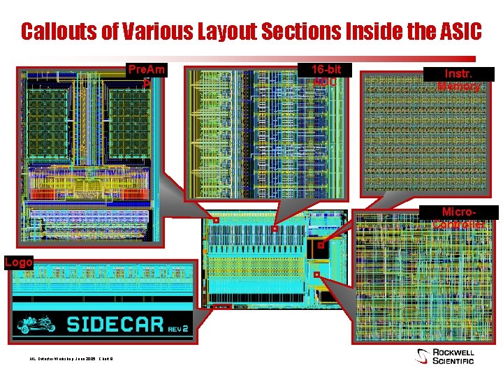
Callouts of Various Layout Sections Inside the ASIC Pre. Am p 16 -bit ADC Instr. Memory Micro. Controller Logo ML, Detector Workshop, June 2005 Chart 9

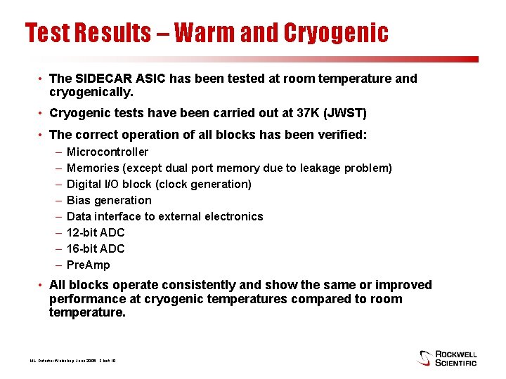
Test Results – Warm and Cryogenic • The SIDECAR ASIC has been tested at room temperature and cryogenically. • Cryogenic tests have been carried out at 37 K (JWST) • The correct operation of all blocks has been verified: – – – – Microcontroller Memories (except dual port memory due to leakage problem) Digital I/O block (clock generation) Bias generation Data interface to external electronics 12 -bit ADC 16 -bit ADC Pre. Amp • All blocks operate consistently and show the same or improved performance at cryogenic temperatures compared to room temperature. ML, Detector Workshop, June 2005 Chart 10

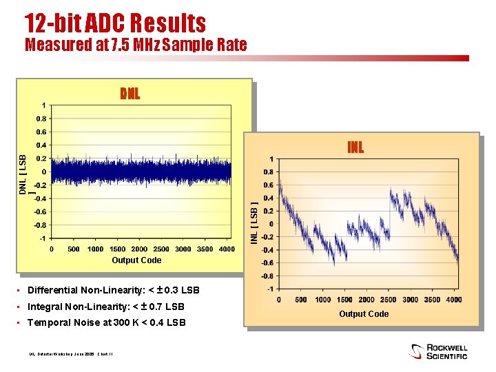
12 -bit ADC Results Measured at 7. 5 MHz Sample Rate DNL INL [ LSB ] DNL [ LSB ] INL Output Code • Differential Non-Linearity: < ± 0. 3 LSB • Integral Non-Linearity: < ± 0. 7 LSB • Temporal Noise at 300 K < 0. 4 LSB ML, Detector Workshop, June 2005 Chart 11 Output Code

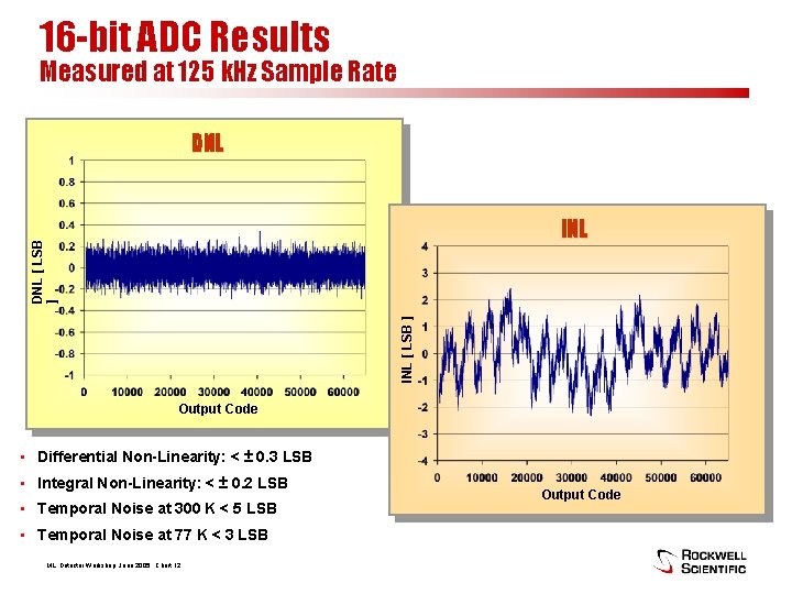
16 -bit ADC Results Measured at 125 k. Hz Sample Rate DNL INL [ LSB ] DNL [ LSB ] INL Output Code • Differential Non-Linearity: < ± 0. 3 LSB • Integral Non-Linearity: < ± 0. 2 LSB • Temporal Noise at 300 K < 5 LSB • Temporal Noise at 77 K < 3 LSB ML, Detector Workshop, June 2005 Chart 12 Output Code

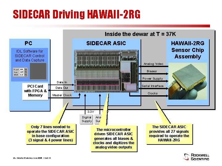
SIDECAR Driving HAWAII-2 RG Inside the dewar at T = 37 K PC SIDECAR ASIC IDL Software for SIDECAR Control and Data Capture Vreset 000 w Dsub 384 w Clock 0 cd w HAWAII-2 RG Sensor Chip Assembly Analog Video Biases Power Supply Data In PCI Card with FPGA & Memory Serial Interface Data Out Clocks Master Clock 3. 3 V Digital Supply Only 7 lines needed to operate the SIDECAR ASIC in base configuration (3 signal & 4 power lines) ML, Detector Workshop, June 2005 Chart 13 3. 3 V Analog Supply The microcontroller driven SIDECAR ASIC generates all biases & clocks and digitizes the analog video outputs The SIDECAR ASIC provides all 27 signals required to operate the HAWAII-2 RG

Noise Results – Differential Operation • HAWAII-2 RG with 2. 5 µm cutoff Hg. Cd. Te • CDS of two consecutive frames • CDS noise: 16 e • Better than conventional controller ML, Detector Workshop, June 2005 Chart 14

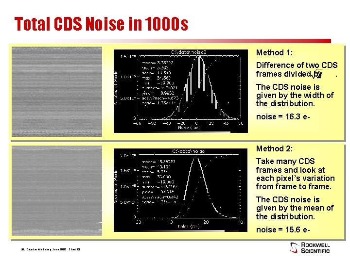
Total CDS Noise in 1000 s Method 1: Difference of two CDS frames divided by. The CDS noise is given by the width of the distribution. noise = 16. 3 e- Method 2: Take many CDS frames and look at each pixel’s variation from frame to frame. The CDS noise is given by the mean of the distribution. noise = 15. 6 e. ML, Detector Workshop, June 2005 Chart 15

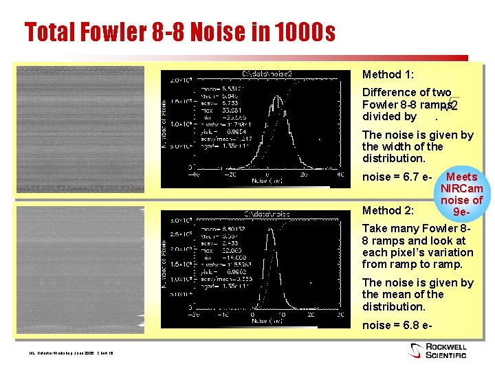
Total Fowler 8 -8 Noise in 1000 s Method 1: Difference of two Fowler 8 -8 ramps divided by. The noise is given by the width of the distribution. noise = 6. 7 e. Method 2: Meets NIRCam noise of 9 e- Take many Fowler 88 ramps and look at each pixel’s variation from ramp to ramp. The noise is given by the mean of the distribution. noise = 6. 8 e. ML, Detector Workshop, June 2005 Chart 16

Total Up-The-Ramp Noise (1000 s) Method 1: Difference of two ramps (22 x 4 frames each) divided by. The noise is given by the width of the distribution. noise = 4. 95 e- Meets NIRSpec noise of 6 e. Method 2: Take many ramps and look at the slope variation from ramp to ramp for each pixel. The noise is given by the mean of the distribution. noise = 5. 2 e. ML, Detector Workshop, June 2005 Chart 17

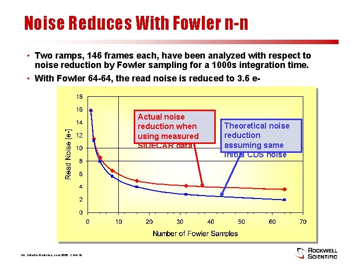
Noise Reduces With Fowler n-n • Two ramps, 146 frames each, have been analyzed with respect to noise reduction by Fowler sampling for a 1000 s integration time. • With Fowler 64 -64, the read noise is reduced to 3. 6 e- Actual noise reduction when using measured SIDECAR data ML, Detector Workshop, June 2005 Chart 18 Theoretical noise reduction assuming same initial CDS noise

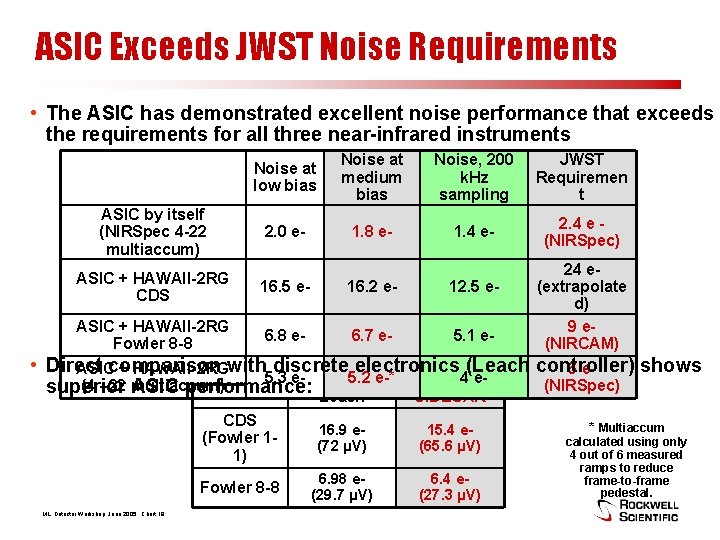
ASIC Exceeds JWST Noise Requirements • The ASIC has demonstrated excellent noise performance that exceeds the requirements for all three near-infrared instruments ASIC by itself (NIRSpec 4 -22 multiaccum) Noise at low bias Noise at medium bias Noise, 200 k. Hz sampling JWST Requiremen t 2. 0 e- 1. 8 e- 1. 4 e- 2. 4 e (NIRSpec) ASIC + HAWAII-2 RG CDS 16. 5 e- 16. 2 e- 12. 5 e- ASIC + HAWAII-2 RG Fowler 8 -8 6. 8 e- 6. 7 e- 5. 1 e- 24 e(extrapolate d) 9 e(NIRCAM) • Direct shows ASICcomparison + HAWAII-2 RGwith discrete electronics (Leach controller) 6 e 5. 3 e 5. 2 e-* 4 e(4 – 22 multiaccum) (NIRSpec) superior ASIC performance: Leach SIDECAR ML, Detector Workshop, June 2005 Chart 19 CDS (Fowler 11) 16. 9 e(72 µV) 15. 4 e(65. 6 µV) Fowler 8 -8 6. 98 e(29. 7 µV) 6. 4 e(27. 3 µV) * Multiaccum calculated using only 4 out of 6 measured ramps to reduce frame-to-frame pedestal.

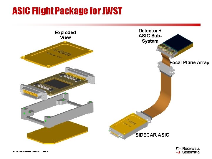
ASIC Flight Package for JWST Exploded View Detector + ASIC Sub. System Focal Plane Array SIDECAR ASIC ML, Detector Workshop, June 2005 Chart 20

Conclusion • Full functionality has been demonstrated • Noise performance is comparable to or exceeds performance of conventional controllers • Operates from room temperature down to 30 K • Significantly smaller and lower power than discrete electronics: – Can be placed inside the dewar fully digital camera system – The solution for large mosaics • First ASIC version showed significant leakage current in the dualport memory – Problem has been fixed in second ASIC revision – Rev 2 ASICs have just arrived at Rockwell Scientific and are currently being tested • ASIC has beenindicate selected JWST as problem the detector controller for – First results thatby the leakage has been completely resolved NIRCAM, NIRSpec and FGS. • ASICs for ground-based astronomy will be available within ~3 months – Cryogenically suitable 337 -pin LGA package – USB-based interface electronics for easy hook-up to a PC – Complete suite of software tools (Assembler, Integrated design&test environment) ML, Detector Workshop, June 2005 Chart 21