Altera vs Xilinx Ognjen eki ogicg yu prof





- Slides: 103

Altera vs. Xilinx Ognjen Šćekić ogi@cg. yu prof. dr Veljko Milutinović vm@etf. bg. ac. yu Ognjen Šćekić 1

Introduction Ognjen Šćekić 2

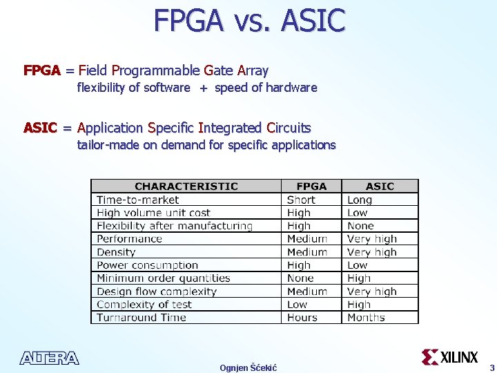
FPGA vs. ASIC FPGA = Field Programmable Gate Array flexibility of software + speed of hardware ASIC = Application Specific Integrated Circuits tailor-made on demand for specific applications Ognjen Šćekić 3

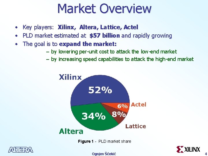
Market Overview • Key players: Xilinx, Altera, Lattice, Actel • PLD market estimated at $57 billion and rapidly growing • The goal is to expand the market: – by lowering per-unit cost to attack the low-end market – by increasing speed capabilities to attack the high-end market Figure 1 - PLD market share Ognjen Šćekić 4

About Xilinx • Pronounced "zylinks" • Founded in 1984 • Employs around 2, 600 people. • Claims more than half the world demand for FPGAs. • Partners with leading semiconductor manufacturers such as IBM Microelectronics, UMC and Seiko. • Xilinx is the net market leader at the moment Ognjen Šćekić 5

About Altera • Founded in 1983. • Introduced look-up table based architecture in 1992 • Second greatest FPGA manufacturer • Strategic partner is TSMC Ognjen Šćekić 6

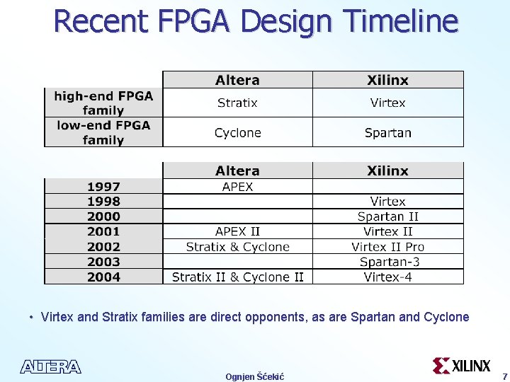
Recent FPGA Design Timeline • Virtex and Stratix families are direct opponents, as are Spartan and Cyclone Ognjen Šćekić 7

Key Factors For Comparing FPGAs • Fabrication process • Logic density • Clock management • On-chip memory • DSP capabilities • I/O compatibility • Software support & other design services Ognjen Šćekić 8

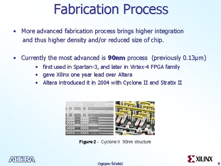
Fabrication Process • More advanced fabrication process brings higher integration and thus higher density and/or reduced size of chip. • Currently the most advanced is 90 nm process (previously 0. 13μm) • • • first used in Spartan-3, and later in Virtex-4 FPGA family gave Xilinx one year lead over Altera introduced it in 2004 with Cyclone II and Stratix II Figure 2 - Cyclone II 90 nm structure Ognjen Šćekić 9

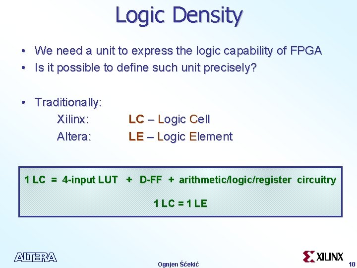
Logic Density • We need a unit to express the logic capability of FPGA • Is it possible to define such unit precisely? • Traditionally: Xilinx: Altera: LC – Logic Cell LE – Logic Element 1 LC = 4 -input LUT + D-FF + arithmetic/logic/register circuitry 1 LC = 1 LE Ognjen Šćekić 10

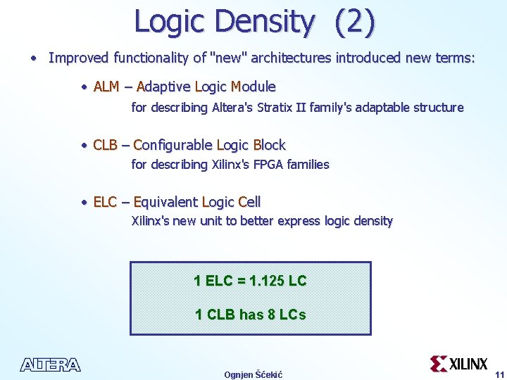
Logic Density (2) • Improved functionality of "new" architectures introduced new terms: • ALM – Adaptive Logic Module for describing Altera's Stratix II family's adaptable structure • CLB – Configurable Logic Block for describing Xilinx's FPGA families • ELC – Equivalent Logic Cell Xilinx's new unit to better express logic density 1 ELC = 1. 125 LC 1 CLB has 8 LCs Ognjen Šćekić 11

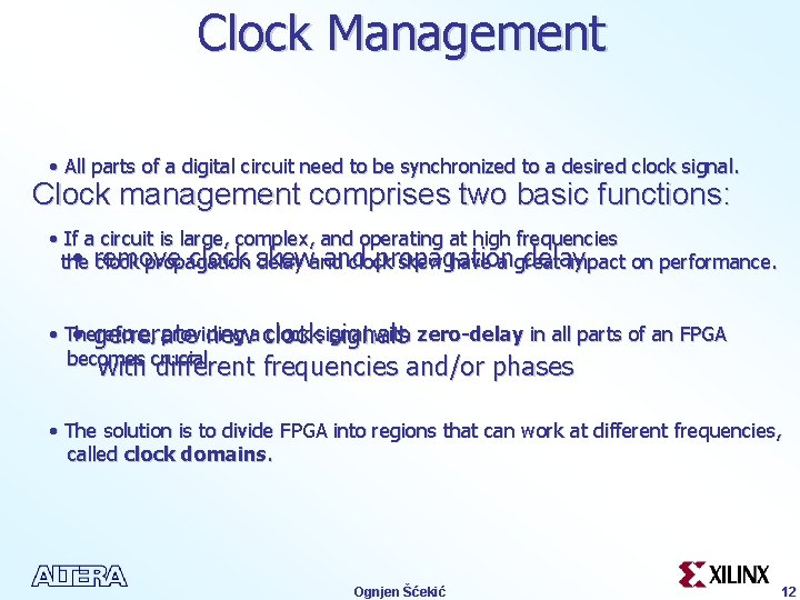
Clock Management • All parts of a digital circuit need to be synchronized to a desired clock signal. Clock management comprises two basic functions: • If a circuit is large, complex, and operating at high frequencies • remove clock skew and propagation delay the clock propagation delay and clock skew have a great impact on performance. • Therefore, providing clock signal with zero-delay in all parts of an FPGA • generate newa clock signals becomes crucial. with different frequencies and/or phases • The solution is to divide FPGA into regions that can work at different frequencies, called clock domains. Ognjen Šćekić 12

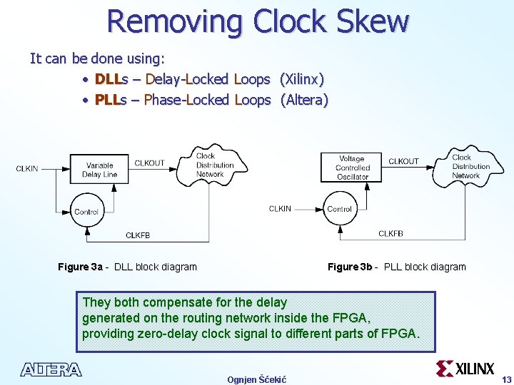
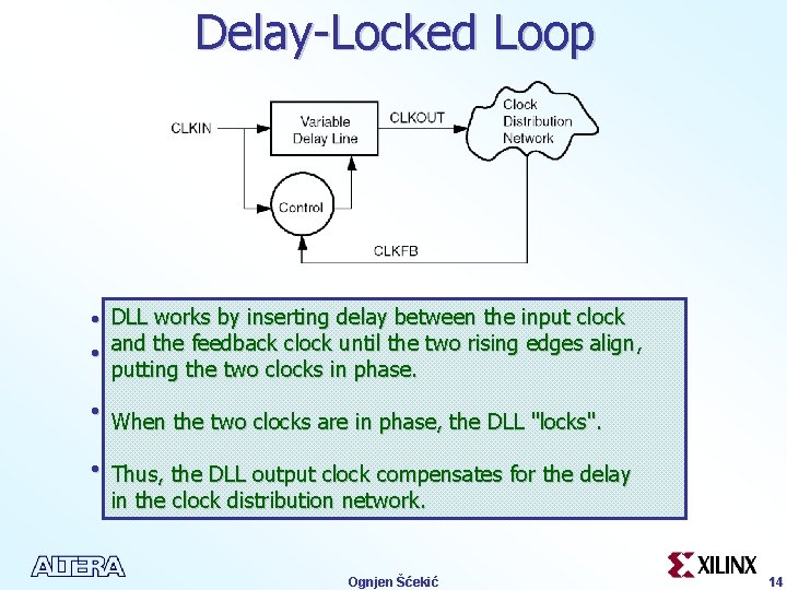
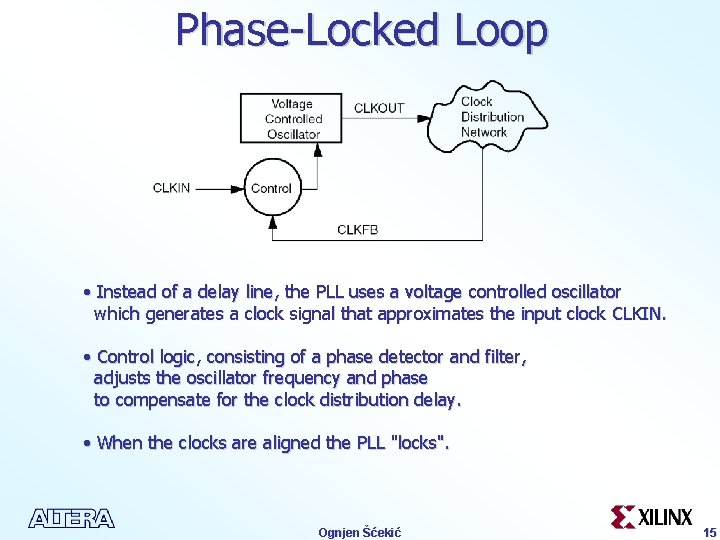
Removing Clock Skew It can be done using: • DLLs – Delay-Locked Loops (Xilinx) • PLLs – Phase-Locked Loops (Altera) Figure 3 a - DLL block diagram Figure 3 b - PLL block diagram They both compensate for the delay generated on the routing network inside the FPGA, providing zero-delay clock signal to different parts of FPGA. Ognjen Šćekić 13

Delay-Locked Loop DLL works by inserting delay between input clock • Delay-line produces a delayed version of thethe input clock CLKIN. and the feedback clock routes until the edges align, • Clock distribution network thetwo clockrising to FPGA interior putting two clocks phase. and to thethe feedback CLKFBinpin. • Control logic sample the input clock and the feedback clock When the two clocks are in phase, the DLL "locks". in order to adjust the delay line. • Delay-line on an clock array compensates of delay elements, Thus, theconsists DLL output for the delay typically CMOSdistribution voltage-controlled inverters connected in series. in the clock network. Ognjen Šćekić 14

Phase-Locked Loop • Instead of a delay line, the PLL uses a voltage controlled oscillator which generates a clock signal that approximates the input clock CLKIN. • Control logic, consisting of a phase detector and filter, adjusts the oscillator frequency and phase to compensate for the clock distribution delay. • When the clocks are aligned the PLL "locks". Ognjen Šćekić 15

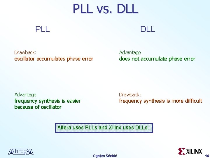
PLL vs. DLL PLL Drawback: Advantage: Drawback: oscillator accumulates phase error frequency synthesis is easier because of oscillator does not accumulate phase error frequency synthesis is more difficult Altera uses PLLs and Xilinx uses DLLs. Ognjen Šćekić 16

Clock Generation & Phase Shifting • Beside clock skew elimination, DLLs (PLLs) are also used for: • frequency multiplication and division • duty-cycle regulation • phase shifting • Clock managers need to be resistant to temperature/voltage variations. Clock manipulation dramatically simplifies the design and improves performance. At the same time it provides many design alternatives. Ognjen Šćekić 17

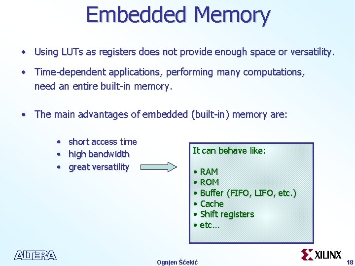
Embedded Memory • Using LUTs as registers does not provide enough space or versatility. • Time-dependent applications, performing many computations, need an entire built-in memory. • The main advantages of embedded (built-in) memory are: • • • short access time high bandwidth great versatility It can behave like: • RAM • ROM • Buffer (FIFO, LIFO, etc. ) • Cache • Shift registers • etc… Ognjen Šćekić 18

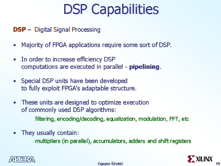
DSP Capabilities DSP – Digital Signal Processing • Majority of FPGA applications require some sort of DSP. • In order to increase efficiency DSP computations are executed in parallel - pipelining. • Special DSP units have been developed to fully exploit FPGA's adaptable structure. • These units are designed to optimize execution of commonly used DSP algorithms: filtering, encoding/decoding, equalization, modulation, FFT, etc • They usually contain: multipliers (in parallel), accumulators, adders and shift registers Ognjen Šćekić 19

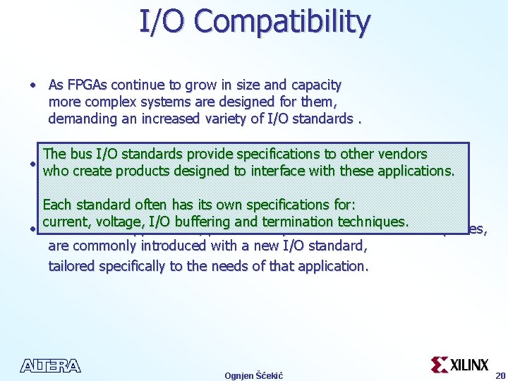
I/O Compatibility • As FPGAs continue to grow in size and capacity more complex systems are designed for them, demanding an increased variety of I/O standards. The bus I/O standards provide specifications to other vendors • Furthermore, as system-clock speeds continue to increase, who create products designed to interface with these applications. the need for high-performance I/O becomes more important. Each standard often has its own specifications for: I/O buffering and termination techniques. • current, Modern voltage, bus applications, pioneered by the most influential companies, are commonly introduced with a new I/O standard, tailored specifically to the needs of that application. Ognjen Šćekić 20

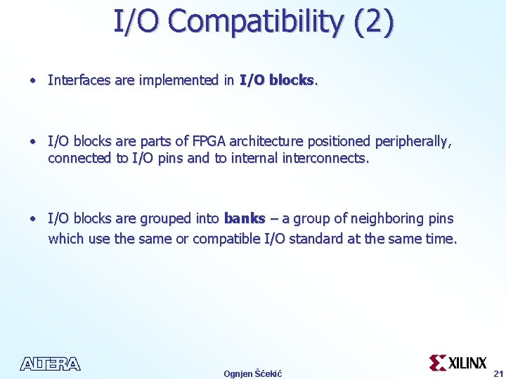
I/O Compatibility (2) • Interfaces are implemented in I/O blocks. • I/O blocks are parts of FPGA architecture positioned peripherally, connected to I/O pins and to internal interconnects. • I/O blocks are grouped into banks – a group of neighboring pins which use the same or compatible I/O standard at the same time. Ognjen Šćekić 21

I/O Compatibility (3) • An I/O block usually contains: ü programmable I/O buffers Programmable so they could adjust to different I/O standards. ü D-FFs Used as optional delay elements or registers. ü pull-up/down resistors Used to assert or de-assert pins that would otherwise float. ü delay array Provides a programmable delay of I/O signals. ü keeper circuit Keeps the last state on a bus if all other drivers are in High-Z state. Ognjen Šćekić 22

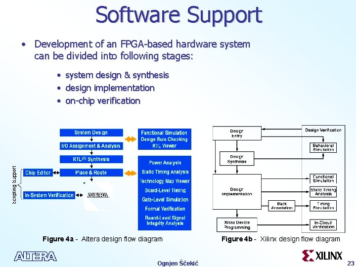
Software Support • Development of an FPGA-based hardware system can be divided into following stages: • system design & synthesis • design implementation • on-chip verification Figure 4 a - Altera design flow diagram Ognjen Šćekić Figure 4 b - Xilinx design flow diagram 23

System Design Stage • Begins with the design entry phase using: • HDL – Hardware Description Language (like VHDL or Verilog) • schematic editor • Software solutions offer complete integrated environments for this stage. • A wide variety of FPGA-ready component libraries are available ranging from simple processors, peripheral components, controllers, down to general logic (gates, counters, decoders, etc). • Software support hierarchical design entry. Ognjen Šćekić 24

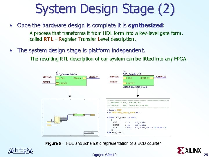
System Design Stage (2) • Once the hardware design is complete it is synthesized: A process that transforms it from HDL form into a low-level gate form, called RTL – Register Transfer Level description. • The system design stage is platform independent. The resulting RTL description of our system can be fitted into any FPGA. Figure 5 - HDL and schematic representation of a BCD counter Ognjen Šćekić 25

Design Implementation Stage • Commonly called Place-And-Route stage. • Place-And-Route tools take the input RTL netlist for the design and map the logic into the architectural resources of the FPGA. • Then, the best location for these blocks is found, based on their interconnections and desired performance. • Finally, the interconnects are routed, and pins assigned. Ognjen Šćekić 26

Design Implementation Stage (2) • This stage is platform-dependent, since our design is implemented in an actual FPGA architecture. • Therefore, place-and-route tools are developed by the FPGA vendors. • They are developed to take full advantage of FPGA architecture, and to provide optimum performance for a given design. • Many analysis and simulation tools are provided for this stage. The result of this stage is a configuration file which is loaded into FPGA at startup Ognjen Šćekić 27

On-Chip Verification Stage • This stage is executed once the design has been loaded into the FPGA. • It gives the developer the possibility for real-world debugging. • Special cables are supplied with FPGA development kits, for connecting FPGAs to a PC or a workstation. • This provides means for reading contents of internal registers and memory. Ognjen Šćekić 28

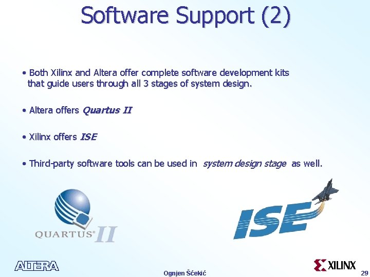
Software Support (2) • Both Xilinx and Altera offer complete software development kits that guide users through all 3 stages of system design. • Altera offers Quartus II • Xilinx offers ISE • Third-party software tools can be used in system design stage as well. Ognjen Šćekić 29

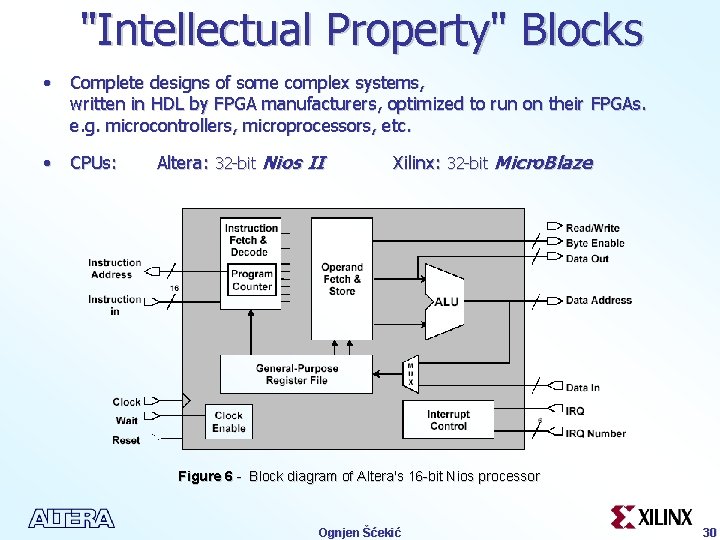
"Intellectual Property" Blocks • Complete designs of some complex systems, written in HDL by FPGA manufacturers, optimized to run on their FPGAs. e. g. microcontrollers, microprocessors, etc. • CPUs: Altera: 32 -bit Nios II Xilinx: 32 -bit Micro. Blaze Figure 6 - Block diagram of Altera's 16 -bit Nios processor Ognjen Šćekić 30

Volume Production Solutions • When FPGA based designs move in volume production the main issue is cost reduction! • Xilinx and Altera have different approaches: Altera Xilinx offers specialized a service called Easy. Path Hard. Copy FPGAs: : It is a migration path from the FPGA to structured ASIC. Once the clients have developedcell their system (on FPGA, Altera developed a fine-grained structure HCells ) ASICs they send it to Xilinx. the logic elements (LEs) of Altera’s FPGAs. which perfectly match That Stratix LEsget areback mapped to equivalent logic elements After way 8 weeks they the optimized FPGAs in theexactly corresponding device. with the same. Hard. Copy functionality. If a Stratix LE is not used in the FPGA design, Theseit optimized FPGAs are. Hard. Copy 30%-80% less expensive when mass produced, then is not mapped to the device, and theyarepresent replacements ASICs , yielding more efficient mapping offor thestructured prototyped design. and take less time to be completed. Ognjen Šćekić 31

Overviews & Comparisons Ognjen Šćekić 32

low-end FPGA family Ognjen Šćekić 33

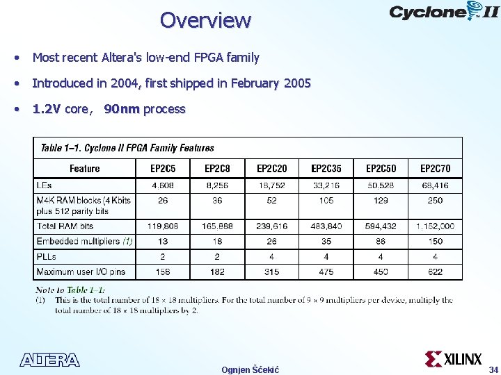
Overview • Most recent Altera's low-end FPGA family • Introduced in 2004, first shipped in February 2005 • 1. 2 V core, 90 nm process Ognjen Šćekić 34

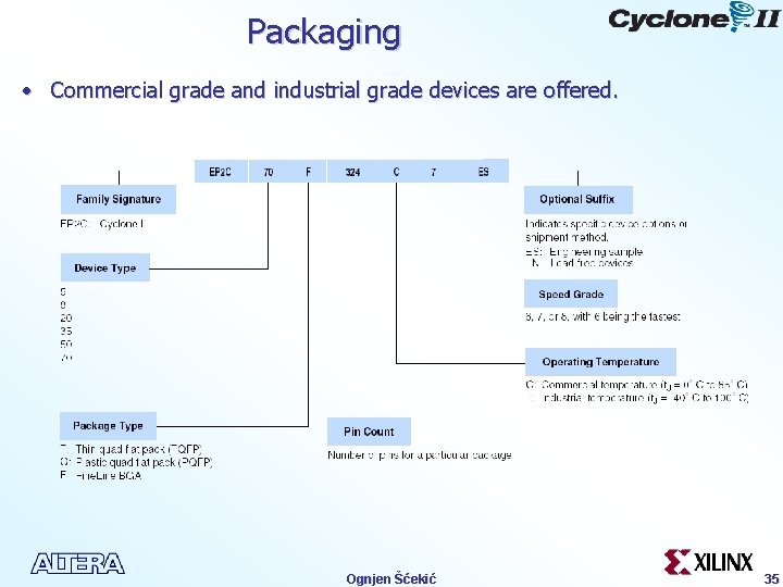
Packaging • Commercial grade and industrial grade devices are offered. Ognjen Šćekić 35

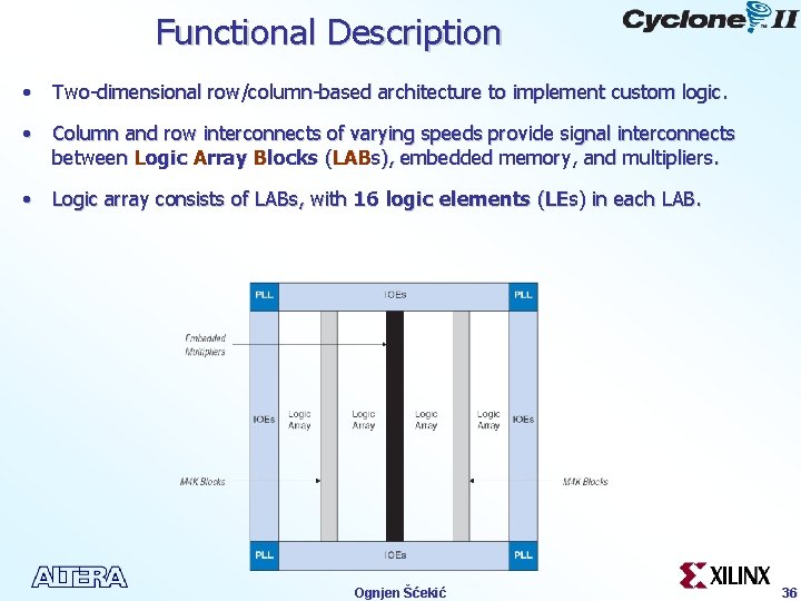
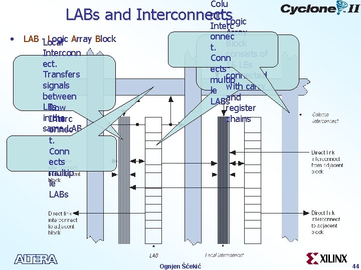
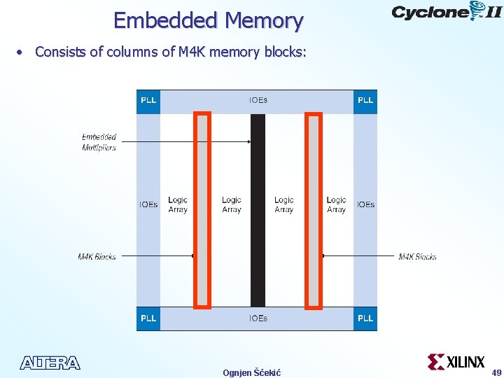
Functional Description • Two-dimensional row/column-based architecture to implement custom logic. • Column and row interconnects of varying speeds provide signal interconnects between Logic Array Blocks (LABs), embedded memory, and multipliers. • Logic array consists of LABs, with 16 logic elements (LEs) in each LAB. Ognjen Šćekić 36

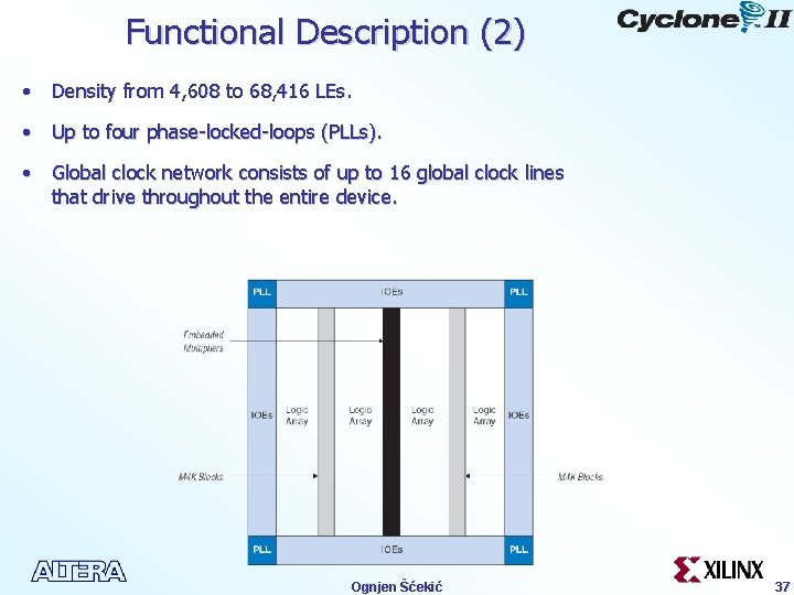
Functional Description (2) • Density from 4, 608 to 68, 416 LEs. • Up to four phase-locked-loops (PLLs). • Global clock network consists of up to 16 global clock lines that drive throughout the entire device. Ognjen Šćekić 37

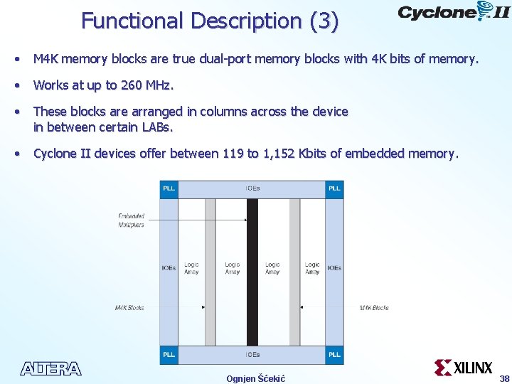
Functional Description (3) • M 4 K memory blocks are true dual-port memory blocks with 4 K bits of memory. • Works at up to 260 MHz. • These blocks are arranged in columns across the device in between certain LABs. • Cyclone II devices offer between 119 to 1, 152 Kbits of embedded memory. Ognjen Šćekić 38

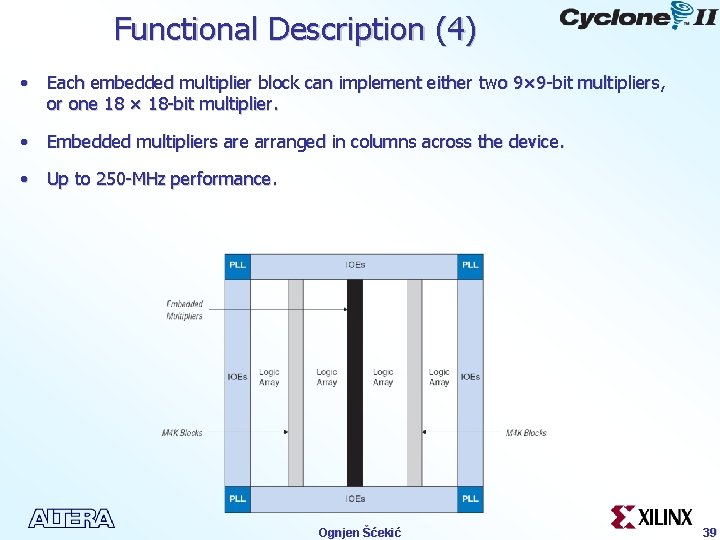
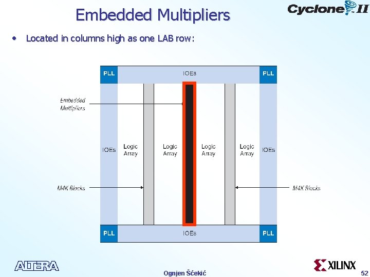
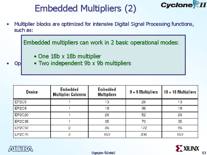
Functional Description (4) • Each embedded multiplier block can implement either two 9× 9 -bit multipliers, or one 18 × 18 -bit multiplier. • Embedded multipliers are arranged in columns across the device. • Up to 250 -MHz performance. Ognjen Šćekić 39

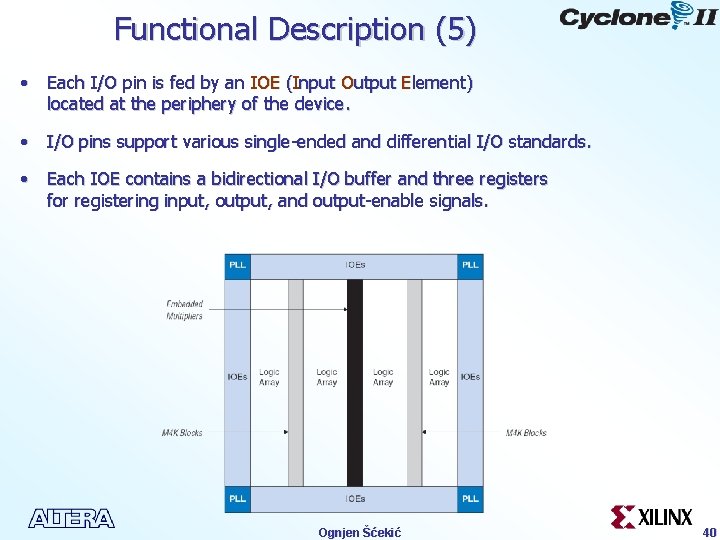
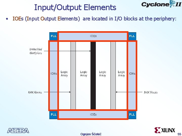
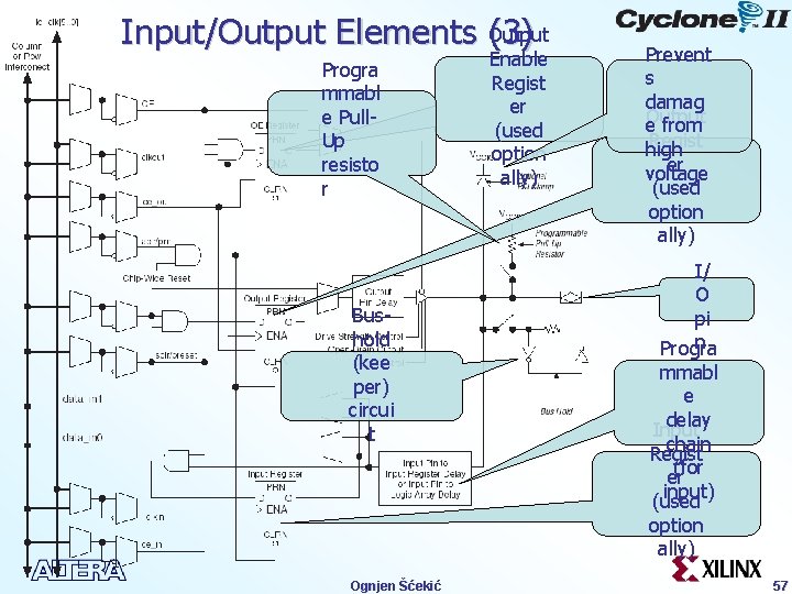
Functional Description (5) • Each I/O pin is fed by an IOE (Input Output Element) located at the periphery of the device. • I/O pins support various single-ended and differential I/O standards. • Each IOE contains a bidirectional I/O buffer and three registers for registering input, output, and output-enable signals. Ognjen Šćekić 40

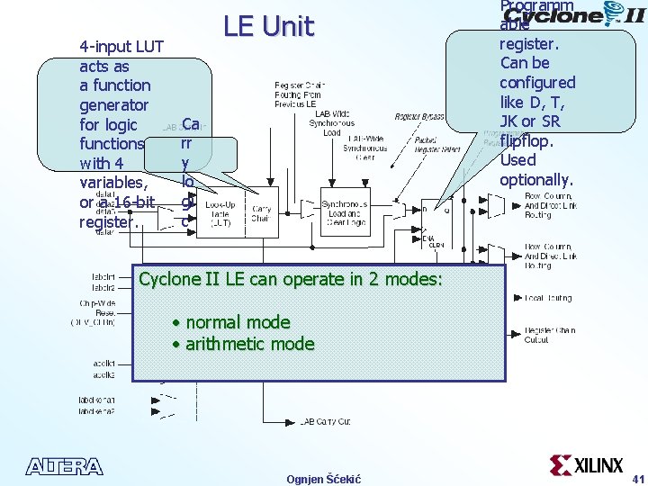
4 -input LUT acts as a function generator for logic functions with 4 variables, or a 16 -bit register. LE Unit Ca rr y lo gi c Programm able register. Can be configured like D, T, JK or SR flipflop. Used optionally. Cyclone II LE can operate in 2 modes: • normal mode • arithmetic mode Ognjen Šćekić 41

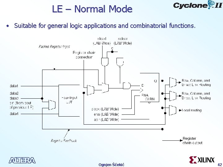
LE – Normal Mode • Suitable for general logic applications and combinatorial functions. Ognjen Šćekić 42

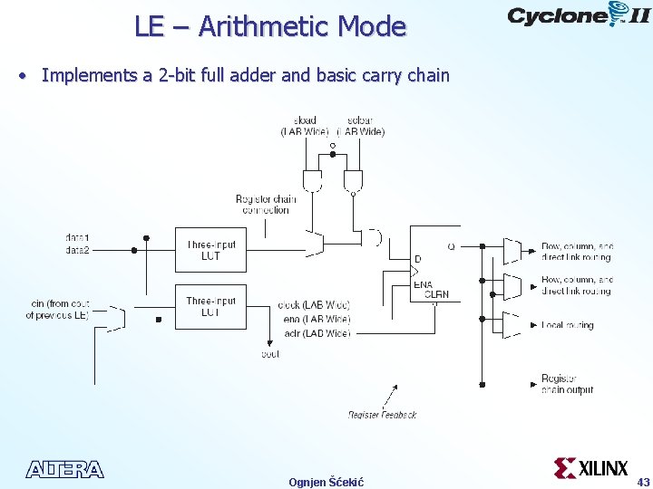
LE – Arithmetic Mode • Implements a 2 -bit full adder and basic carry chain Ognjen Šćekić 43

Colu mn Logic Interc Array onnec t. Block consists of Conn ects 16 LEs connected multip le with carry LABsand register chains LABs and Interconnects • LAB -Local Logic Array Block Interconn ect. Transfers signals between LEs Row in. Interc the same LAB onnec t. Conn ects multip le LABs Ognjen Šćekić 44

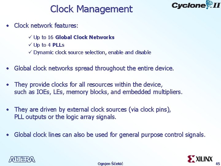
Clock Management • Clock network features: ü Up to 16 Global Clock Networks ü Up to 4 PLLs ü Dynamic clock source selection, enable and disable • Global clock networks spread throughout the entire device. • They provide clocks for all resources within the device, such as IOEs, LEs, memory blocks, and embedded multipliers. • They are driven by external clock sources (via clock pins), PLL outputs or the logic array signals. • Global clock lines can also be used for general purpose control signals. Ognjen Šćekić 45

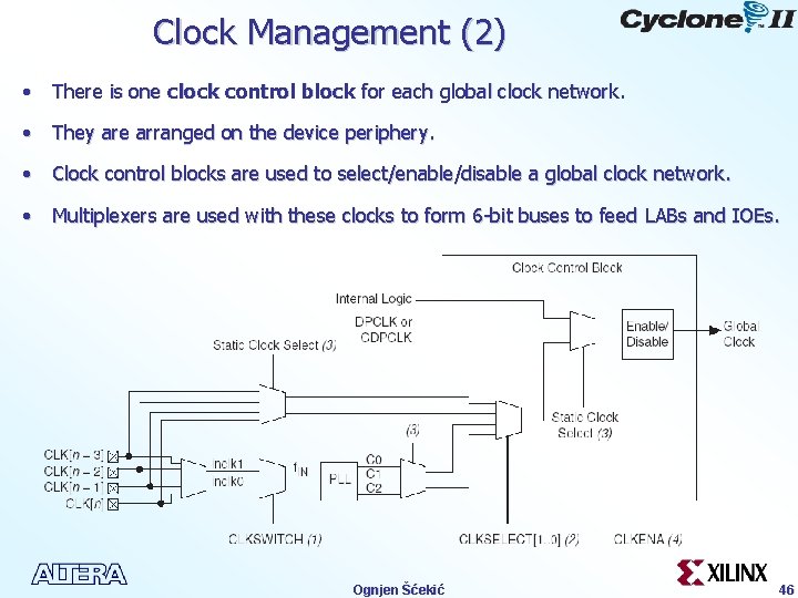
Clock Management (2) • There is one clock control block for each global clock network. • They are arranged on the device periphery. • Clock control blocks are used to select/enable/disable a global clock network. • Multiplexers are used with these clocks to form 6 -bit buses to feed LABs and IOEs. Ognjen Šćekić 46

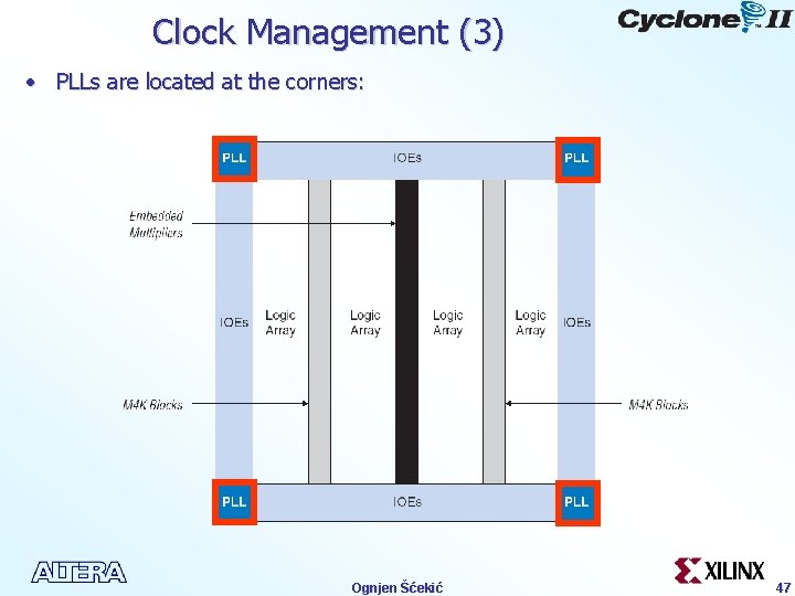
Clock Management (3) • PLLs are located at the corners: Ognjen Šćekić 47

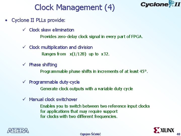
Clock Management (4) • Cyclone II PLLs provide: ü Clock skew elimination Provides zero-delay clock signal in every part of FPGA. ü Clock multiplication and division Ranges from x(1/128) up to x 32. ü Phase shifting Programmable phase shifts in increments of at least 45°. ü Programmable duty-cycle Generate clock outputs with a variable duty cycle ü Manual clock switchover Enables you to switch between two reference input clocks for applications that may require support for clocks with two different frequencies. Ognjen Šćekić 48

Embedded Memory • Consists of columns of M 4 K memory blocks: Ognjen Šćekić 49

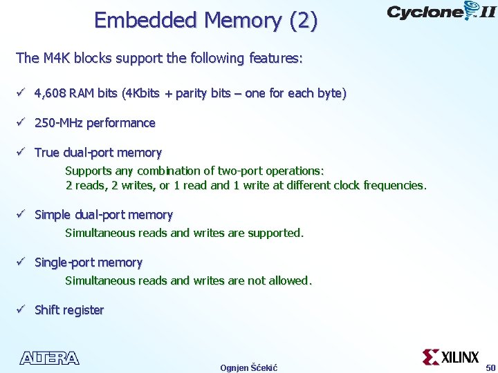
Embedded Memory (2) The M 4 K blocks support the following features: ü 4, 608 RAM bits (4 Kbits + parity bits – one for each byte) ü 250 -MHz performance ü True dual-port memory Supports any combination of two-port operations: 2 reads, 2 writes, or 1 read and 1 write at different clock frequencies. ü Simple dual-port memory Simultaneous reads and writes are supported. ü Single-port memory Simultaneous reads and writes are not allowed. ü Shift register Ognjen Šćekić 50

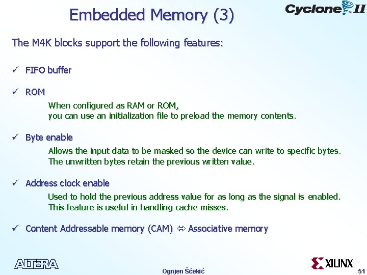
Embedded Memory (3) The M 4 K blocks support the following features: ü FIFO buffer ü ROM When configured as RAM or ROM, you can use an initialization file to preload the memory contents. ü Byte enable Allows the input data to be masked so the device can write to specific bytes. The unwritten bytes retain the previous written value. ü Address clock enable Used to hold the previous address value for as long as the signal is enabled. This feature is useful in handling cache misses. ü Content Addressable memory (CAM) Associative memory Ognjen Šćekić 51

Embedded Multipliers • Located in columns high as one LAB row: Ognjen Šćekić 52

Embedded Multipliers (2) • Multiplier blocks are optimized for intensive Digital Signal Processing functions, such as: finite impulse response (FIR) filters, Fast Fourier Transform (FFT), Embedded multipliers can work in 2 basic Discrete Cosine Transform (DCT) functions, etc. operational modes: • One 18 b x 18 b multiplier • Operate • at. Two up toindependent 250 MHz. 9 b x 9 b multipliers Ognjen Šćekić 53

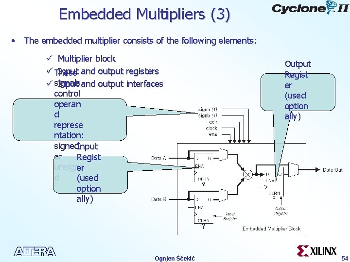
Embedded Multipliers (3) • The embedded multiplier consists of the following elements: ü Multiplier block ü These Input and output registers ü signals Input and output interfaces control operan d represe ntation: signed. Input or Regist unsigne er d (used option ally) Ognjen Šćekić Output Regist er (used option ally) 54

Input/Output Elements • IOEs (Input Output Elements) are located in I/O blocks at the periphery: Ognjen Šćekić 55

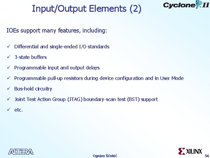
Input/Output Elements (2) IOEs support many features, including: ü Differential and single-ended I/O standards ü 3 -state buffers ü Programmable input and output delays ü Programmable pull-up resistors during device configuration and in User Mode ü Bus-hold circuitry ü Joint Test Action Group (JTAG) boundary-scan test (BST) support ü etc. Ognjen Šćekić 56

Output Input/Output Elements (3) Progra mmabl e Pull. Up resisto r Bushold (kee per) circui t Ognjen Šćekić Enable Regist er (used option ally) Prevent s damag e. Output from Regist high er voltage (used option ally) I/ O pi n Progra mmabl e delay Input chain Regist (for er input) (used option ally) 57

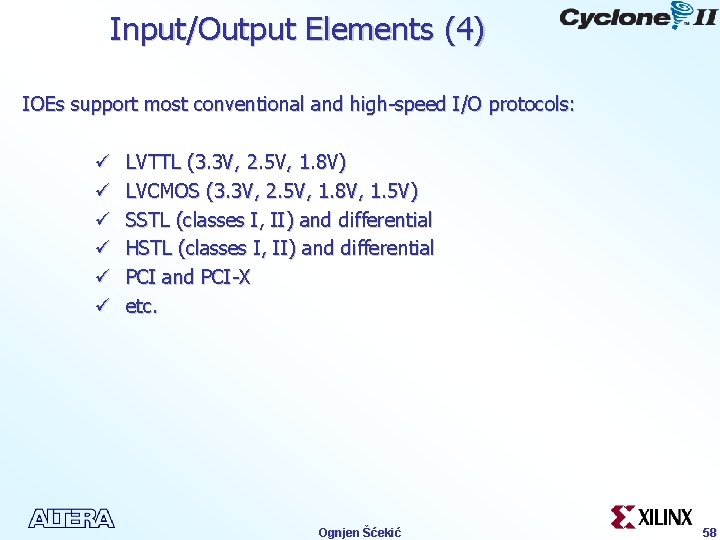
Input/Output Elements (4) IOEs support most conventional and high-speed I/O protocols: ü ü ü LVTTL (3. 3 V, 2. 5 V, 1. 8 V) LVCMOS (3. 3 V, 2. 5 V, 1. 8 V, 1. 5 V) SSTL (classes I, II) and differential HSTL (classes I, II) and differential PCI and PCI-X etc. Ognjen Šćekić 58

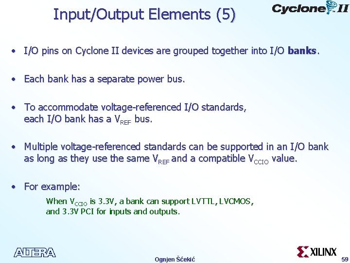
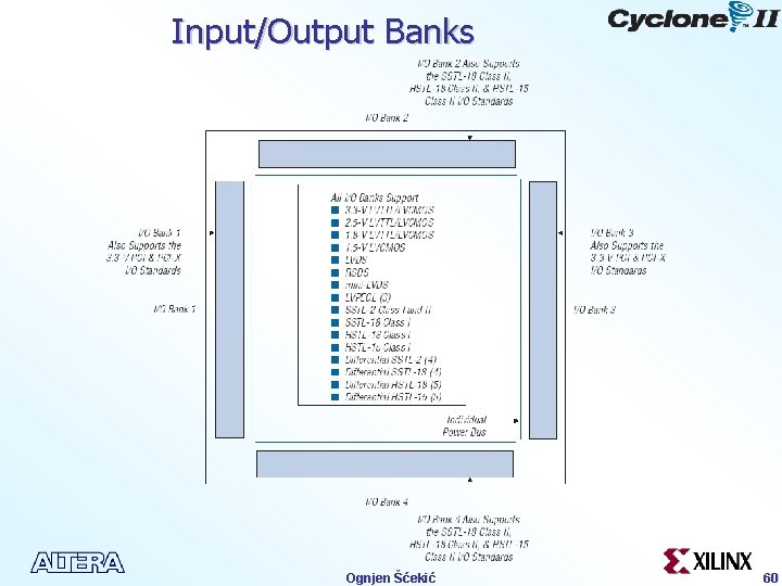
Input/Output Elements (5) • I/O pins on Cyclone II devices are grouped together into I/O banks. • Each bank has a separate power bus. • To accommodate voltage-referenced I/O standards, each I/O bank has a VREF bus. • Multiple voltage-referenced standards can be supported in an I/O bank as long as they use the same VREF and a compatible VCCIO value. • For example: When VCCIO is 3. 3 V, a bank can support LVTTL, LVCMOS, and 3. 3 V PCI for inputs and outputs. Ognjen Šćekić 59

Input/Output Banks Ognjen Šćekić 60

Start-Up Configuration • Logics, circuitry, and routing switches are configured with CMOS SRAM elements that require configuration data to be loaded on each power-up. • Process of physically loading the SRAM data into the device is called: configuration. • During initialization, which occurs immediately after configuration, the device resets registers, enables I/O pins, and begins to operate as a logic device. • Together, configuration and initialization are called: command mode. • Normal device operation is called: user mode. Ognjen Šćekić 61

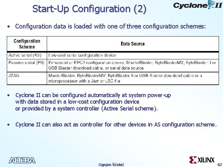
Start-Up Configuration (2) • Configuration data is loaded with one of three configuration schemes: • Cyclone II can be configured automatically at system power-up with data stored in a low-cost configuration device or provided by a system controller (Active Serial scheme). • Cyclone II can also act as controller for other devices in AS configuration scheme. Ognjen Šćekić 62

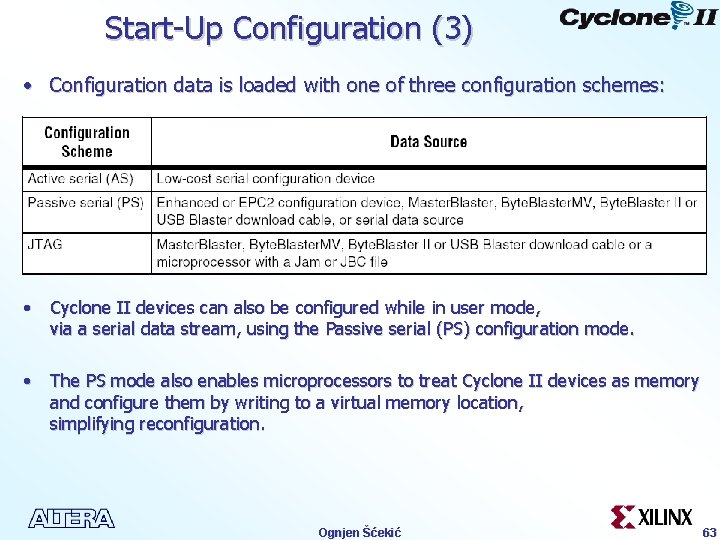
Start-Up Configuration (3) • Configuration data is loaded with one of three configuration schemes: • Cyclone II devices can also be configured while in user mode, via a serial data stream, using the Passive serial (PS) configuration mode. • The PS mode also enables microprocessors to treat Cyclone II devices as memory and configure them by writing to a virtual memory location, simplifying reconfiguration. Ognjen Šćekić 63

low-end FPGA family Ognjen Šćekić 64

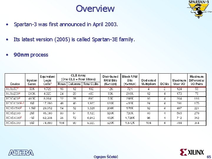
Overview • Spartan-3 was first announced in April 2003. • Its latest version (2005) is called Spartan-3 E family. • 90 nm process Ognjen Šćekić 65

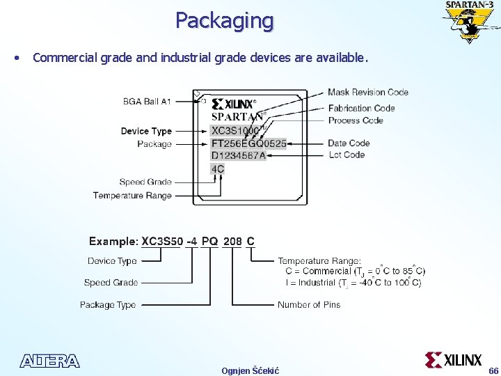
Packaging • Commercial grade and industrial grade devices are available. Ognjen Šćekić 66

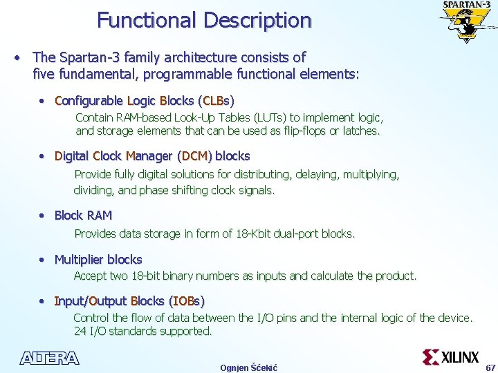
Functional Description • The Spartan-3 family architecture consists of five fundamental, programmable functional elements: • Configurable Logic Blocks (CLBs) Contain RAM-based Look-Up Tables (LUTs) to implement logic, and storage elements that can be used as flip-flops or latches. • Digital Clock Manager (DCM) blocks Provide fully digital solutions for distributing, delaying, multiplying, dividing, and phase shifting clock signals. • Block RAM Provides data storage in form of 18 -Kbit dual-port blocks. • Multiplier blocks Accept two 18 -bit binary numbers as inputs and calculate the product. • Input/Output Blocks (IOBs) Control the flow of data between the I/O pins and the internal logic of the device. 24 I/O standards supported. Ognjen Šćekić 67

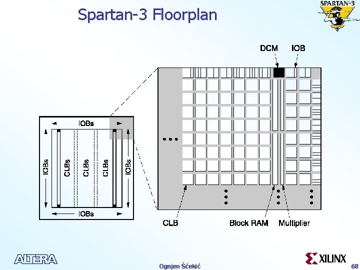
Spartan-3 Floorplan Ognjen Šćekić 68

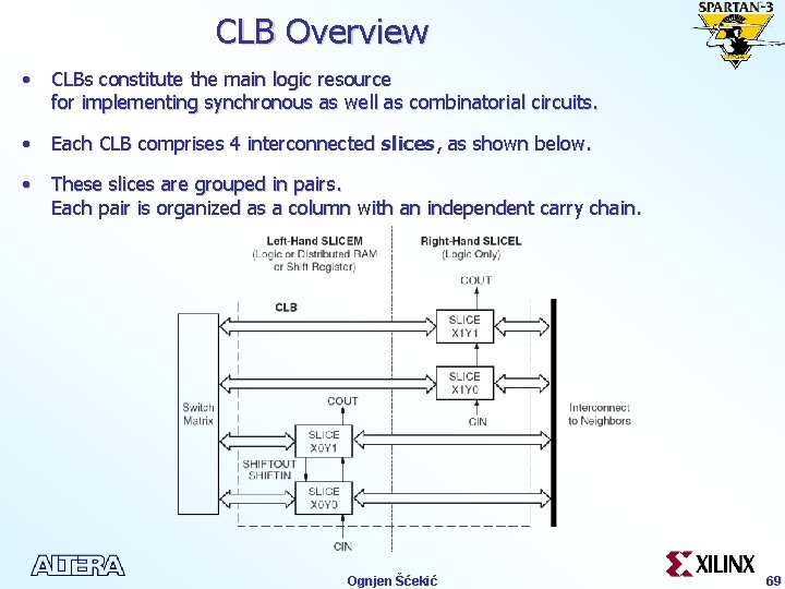
CLB Overview • CLBs constitute the main logic resource for implementing synchronous as well as combinatorial circuits. • Each CLB comprises 4 interconnected slices, as shown below. • These slices are grouped in pairs. Each pair is organized as a column with an independent carry chain. Ognjen Šćekić 69

CLB Overview (2) • All four slices have the following elements in common: ü 2 logic function generators (4 -input LUTs) ü 2 storage elements ü wide-function multiplexers ü carry logic ü arithmetic gates • Both the left-hand right-hand slice pairs use these elements to provide logic, arithmetic, and ROM functions. Ognjen Šćekić 70

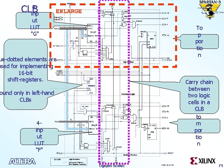
4 CLB inp ENLARGE ut LUT "G" To p por tio n ue-dotted elements are used for implementing 16 -bit shift-registers. Carry chain between two logic cells in a CLB Bot to m por tio n ound only in left-hand CLBs 4 inp ut LUT "F" Ognjen Šćekić 71

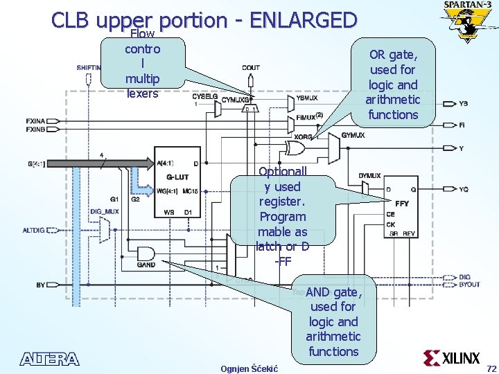
CLB upper portion ENLARGED Flow contro l multip lexers OR gate, used for logic and arithmetic functions Optionall y used register. Program mable as latch or D -FF AND gate, used for logic and arithmetic functions Ognjen Šćekić 72

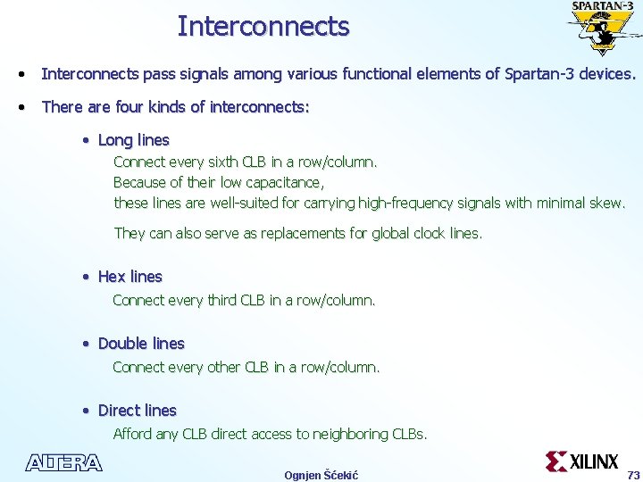
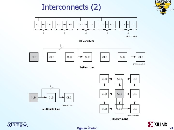
Interconnects • Interconnects pass signals among various functional elements of Spartan-3 devices. • There are four kinds of interconnects: • Long lines Connect every sixth CLB in a row/column. Because of their low capacitance, these lines are well-suited for carrying high-frequency signals with minimal skew. They can also serve as replacements for global clock lines. • Hex lines Connect every third CLB in a row/column. • Double lines Connect every other CLB in a row/column. • Direct lines Afford any CLB direct access to neighboring CLBs. Ognjen Šćekić 73

Interconnects (2) Ognjen Šćekić 74

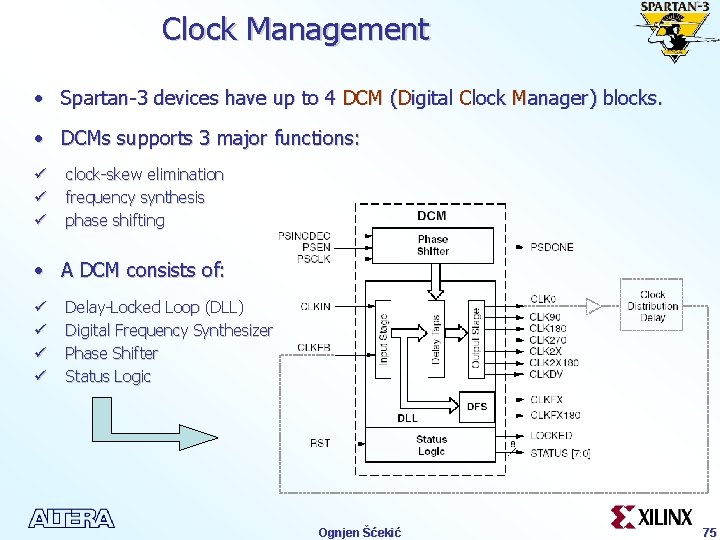
Clock Management • Spartan-3 devices have up to 4 DCM (Digital Clock Manager) blocks. • DCMs supports 3 major functions: ü ü ü clock-skew elimination frequency synthesis phase shifting • A DCM consists of: ü ü Delay-Locked Loop (DLL) Digital Frequency Synthesizer Phase Shifter Status Logic Ognjen Šćekić 75

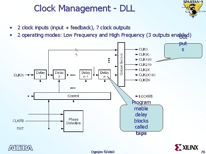
Clock Management - DLL • 2 clock inputs (input + feedback), 7 clock outputs • 2 operating modes: Low Frequency and High Frequency (3 outputs enabled) Out put s Program mable delay blocks called taps Ognjen Šćekić 76

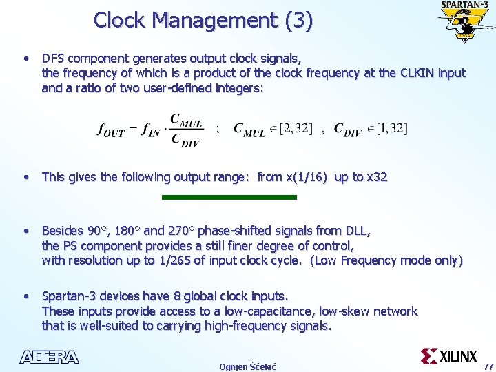
Clock Management (3) • DFS component generates output clock signals, the frequency of which is a product of the clock frequency at the CLKIN input and a ratio of two user-defined integers: • This gives the following output range: from x(1/16) up to x 32 • Besides 90°, 180° and 270° phase-shifted signals from DLL, the PS component provides a still finer degree of control, with resolution up to 1/265 of input clock cycle. (Low Frequency mode only) • Spartan-3 devices have 8 global clock inputs. These inputs provide access to a low-capacitance, low-skew network that is well-suited to carrying high-frequency signals. Ognjen Šćekić 77

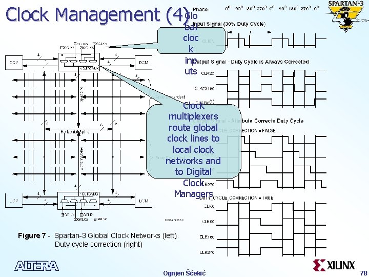
Clock Management (4)Glo bal cloc k inp uts Clock multiplexers route global clock lines to local clock networks and to Digital Clock Managers Figure 7 - Spartan-3 Global Clock Networks (left). Duty cycle correction (right) Ognjen Šćekić 78

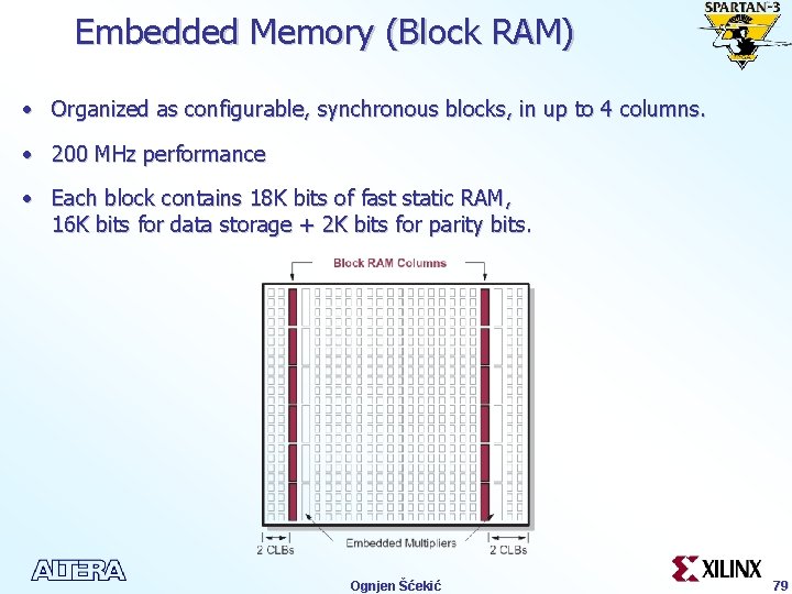
Embedded Memory (Block RAM) • Organized as configurable, synchronous blocks, in up to 4 columns. • 200 MHz performance • Each block contains 18 K bits of fast static RAM, 16 K bits for data storage + 2 K bits for parity bits. Ognjen Šćekić 79

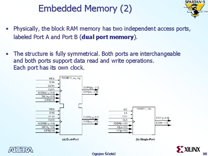
Embedded Memory (2) • Physically, the block RAM memory has two independent access ports, labeled Port A and Port B (dual port memory). • The structure is fully symmetrical. Both ports are interchangeable and both ports support data read and write operations. Each port has its own clock. Ognjen Šćekić 80

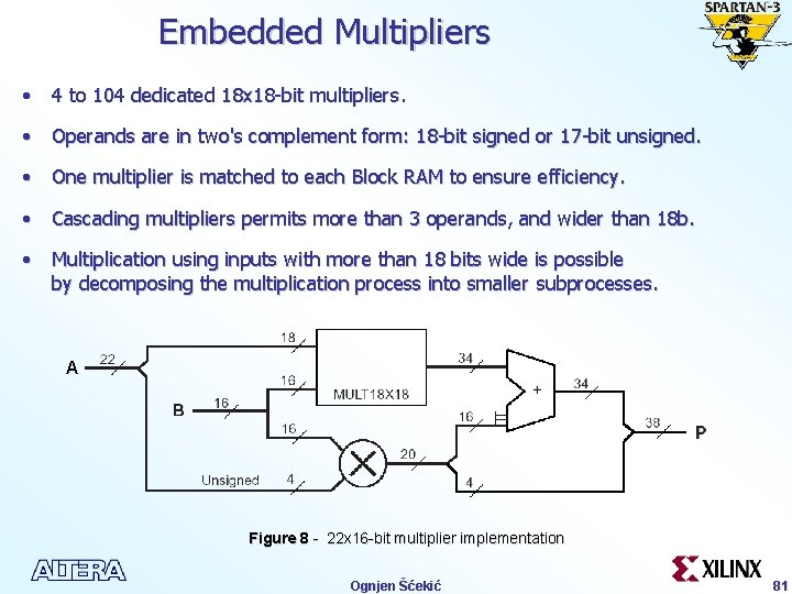
Embedded Multipliers • 4 to 104 dedicated 18 x 18 -bit multipliers. • Operands are in two's complement form: 18 -bit signed or 17 -bit unsigned. • One multiplier is matched to each Block RAM to ensure efficiency. • Cascading multipliers permits more than 3 operands, and wider than 18 b. • Multiplication using inputs with more than 18 bits wide is possible by decomposing the multiplication process into smaller subprocesses. A Figure 8 - 22 x 16 -bit multiplier implementation Ognjen Šćekić 81

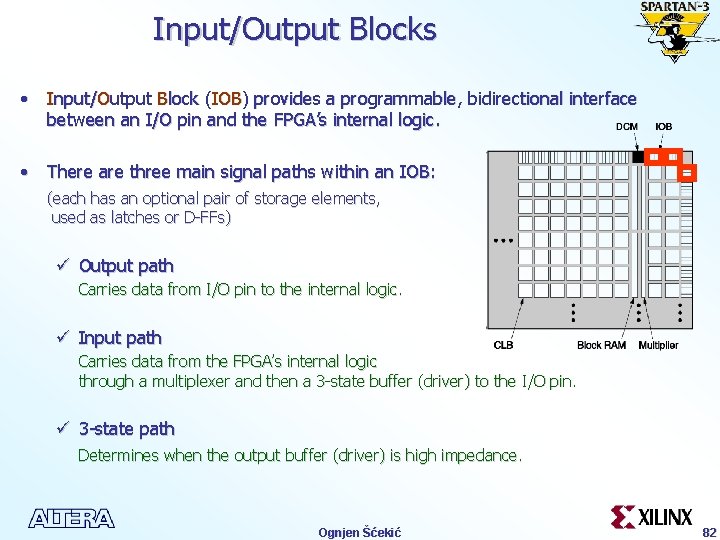
Input/Output Blocks • Input/Output Block (IOB) provides a programmable, bidirectional interface between an I/O pin and the FPGA’s internal logic. • There are three main signal paths within an IOB: (each has an optional pair of storage elements, used as latches or D-FFs) ü Output path Carries data from I/O pin to the internal logic. ü Input path Carries data from the FPGA’s internal logic through a multiplexer and then a 3 -state buffer (driver) to the I/O pin. ü 3 -state path Determines when the output buffer (driver) is high impedance. Ognjen Šćekić 82

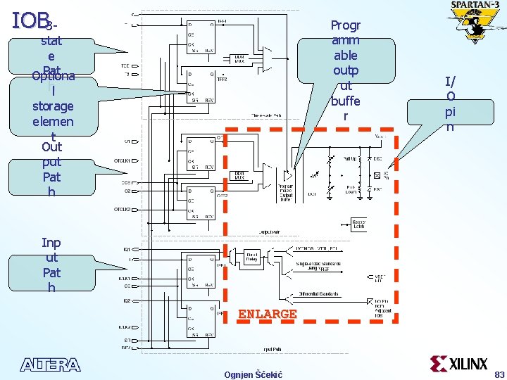
IOB 3 - Progr amm able outp ut buffe r stat e Pat Optiona hl storage elemen t Out put Pat h I/ O pi n Inp ut Pat h ENLARGE Ognjen Šćekić 83

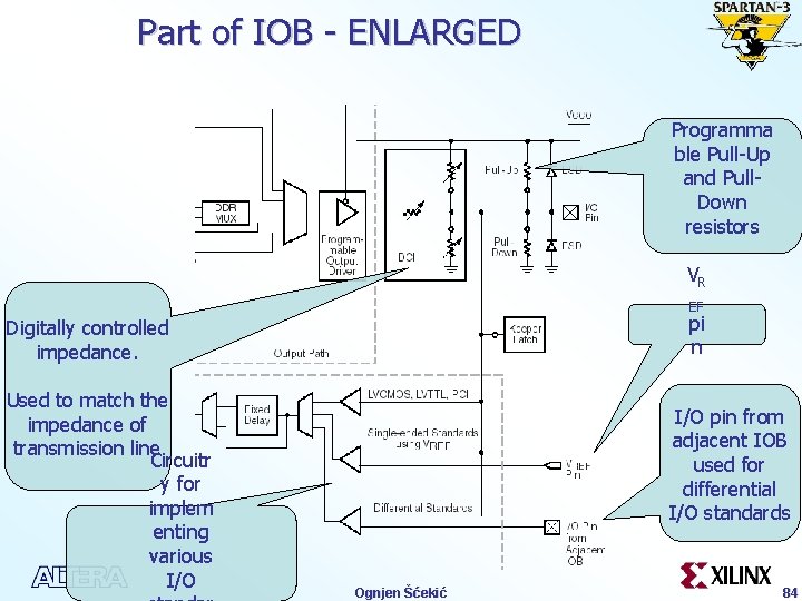
Part of IOB - ENLARGED Programma ble Pull-Up and Pull. Down resistors VR EF pi n Digitally controlled impedance. Used to match the impedance of transmission line Circuitr y for implem enting various I/O pin from adjacent IOB used for differential I/O standards Ognjen Šćekić 84

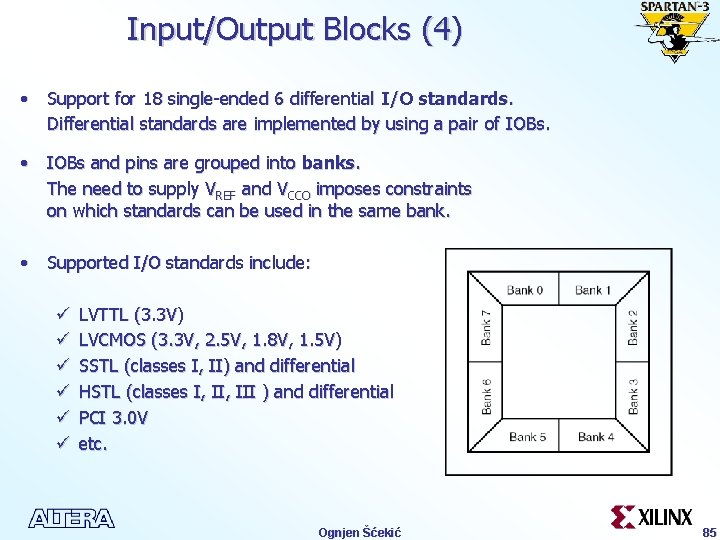
Input/Output Blocks (4) • Support for 18 single-ended 6 differential I/O standards. Differential standards are implemented by using a pair of IOBs. • IOBs and pins are grouped into banks. The need to supply VREF and VCCO imposes constraints on which standards can be used in the same bank. • Supported I/O standards include: ü ü ü LVTTL (3. 3 V) LVCMOS (3. 3 V, 2. 5 V, 1. 8 V, 1. 5 V) SSTL (classes I, II) and differential HSTL (classes I, III ) and differential PCI 3. 0 V etc. Ognjen Šćekić 85

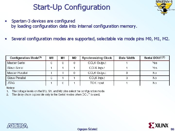
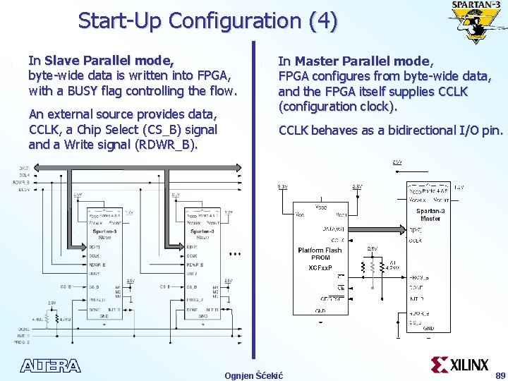
Start-Up Configuration • Spartan-3 devices are configured by loading configuration data into internal configuration memory. • Several configuration modes are supported, selectable via mode pins M 0, M 1, M 2. Ognjen Šćekić 86

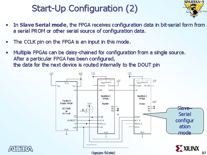
Start-Up Configuration (2) • In Slave Serial mode, the FPGA receives configuration data in bit-serial form from a serial PROM or other serial source of configuration data. • The CCLK pin on the FPGA is an input in this mode. • Multiple FPGAs can be daisy-chained for configuration from a single source. After a particular FPGA has been configured, the data for the next device is routed internally to the DOUT pin Slave– Serial configur ation mode Ognjen Šćekić 87

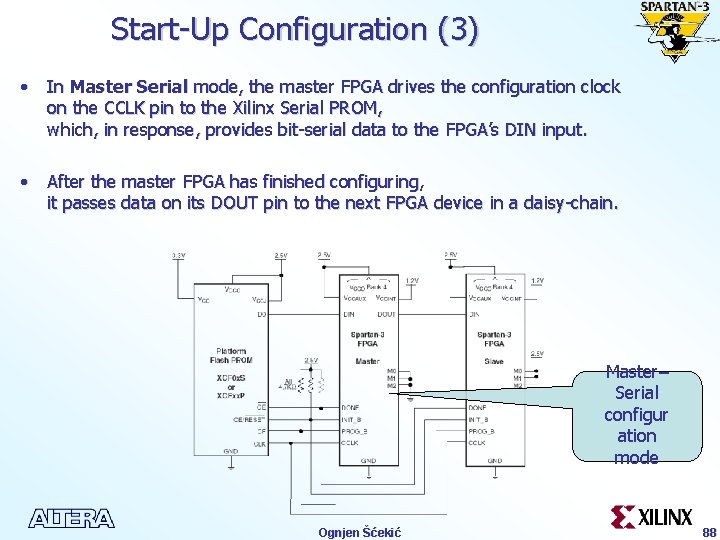
Start-Up Configuration (3) • In Master Serial mode, the master FPGA drives the configuration clock on the CCLK pin to the Xilinx Serial PROM, which, in response, provides bit-serial data to the FPGA’s DIN input. • After the master FPGA has finished configuring, it passes data on its DOUT pin to the next FPGA device in a daisy-chain. Master– Serial configur ation mode Ognjen Šćekić 88

Start-Up Configuration (4) • In Slave Parallel mode, byte-wide data is written into FPGA, with a BUSY flag controlling the flow. • • An external source provides data, CCLK, a Chip Select (CS_B) signal and a Write signal (RDWR_B). In Master Parallel mode, FPGA configures from byte-wide data, and the FPGA itself supplies CCLK (configuration clock). • CCLK behaves as a bidirectional I/O pin. Ognjen Šćekić 89

high-end FPGA family Ognjen Šćekić 90

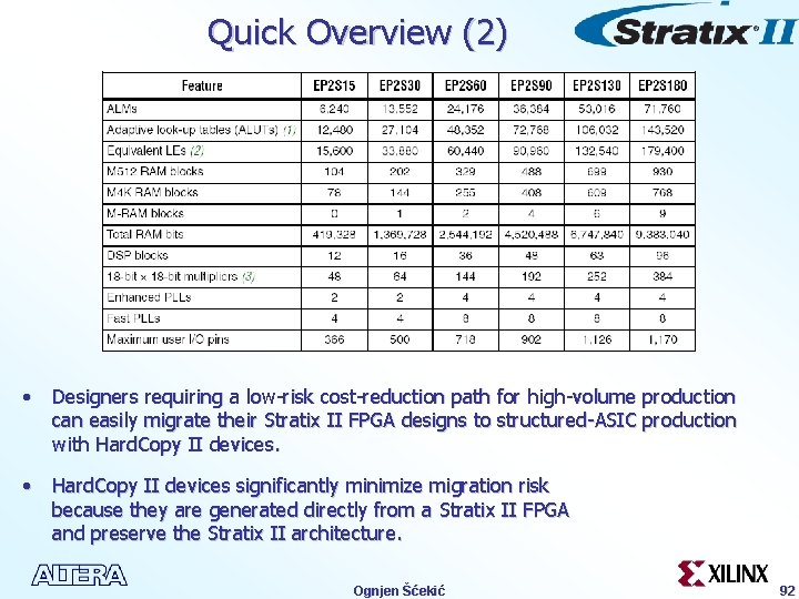
Quick Overview • Launched in February 2004. • 1. 2 V core, 90 nm process • Approaching 180, 000 LEs • Up to 9 Mbits of on-chip, Tri. Matrix memory for memory-demanding applications. • Up to 96 DSP blocks with up to 384 (18 -bit × 18 -bit) multipliers for efficient implementation of high performance filters and other DSP functions. • Various high-speed external memory interfaces are supported. • Complete clock management solution with clock frequency of up to 550 MHz and up to 12 phase-locked loops (PLLs). Ognjen Šćekić 91

Quick Overview (2) • Designers requiring a low-risk cost-reduction path for high-volume production can easily migrate their Stratix II FPGA designs to structured-ASIC production with Hard. Copy II devices. • Hard. Copy II devices significantly minimize migration risk because they are generated directly from a Stratix II FPGA and preserve the Stratix II architecture. Ognjen Šćekić 92

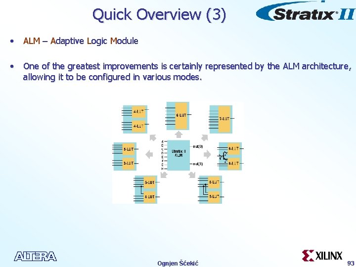
Quick Overview (3) • ALM – Adaptive Logic Module • One of the greatest improvements is certainly represented by the ALM architecture, allowing it to be configured in various modes. Ognjen Šćekić 93

high-end FPGA family Ognjen Šćekić 94

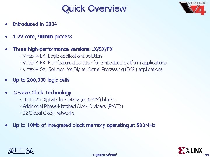
Quick Overview • Introduced in 2004 • 1. 2 V core, 90 nm process • Three high-performance versions LX/SX/FX - Virtex-4 LX: Logic applications solution. - Virtex-4 FX: Full-featured solution for embedded platform applications - Virtex-4 SX: Solution for Digital Signal Processing (DSP) applications • Up to 200, 000 logic cells • Xesium Clock Technology - Up to 20 Digital Clock Manager (DCM) blocks - Additional Phase-Matched Clock Dividers (PMCD) - 32 Global Clock networks • Up to 10 Mb of integrated block memory operating at 500 MHz Ognjen Šćekić 95

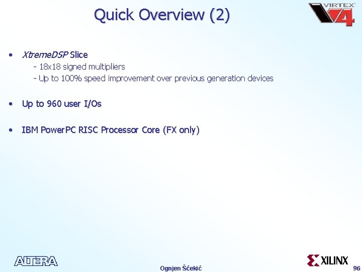
Quick Overview (2) • Xtreme. DSP Slice - 18 x 18 signed multipliers - Up to 100% speed improvement over previous generation devices • Up to 960 user I/Os • IBM Power. PC RISC Processor Core (FX only) Ognjen Šćekić 96

Quick Overview (3) • At the heart of the Virtex-4 family is the new ASMBL architecture. ASMBL – Advanced Silicon Modular Block • This new, highly modular ASMBL architecture makes use of advanced packaging technology and eliminates geometric layout constraints associated with traditional chip design. • Thanks to it, Xilinx can vary the number and ratio of different functional parts to create a family (platform) of different sized devices, each best suited for a certain domain of applications, depending on the desired type of functional attributes. • This approach enables the right feature mix at the lowest cost, and resulted in 3 platforms of Virtex-4 FPGAs – LX, FX, SX. Ognjen Šćekić 97

Altera vs. Xilinx Ognjen Šćekić 98

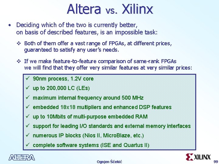
Altera vs. Xilinx • Deciding which of the two is currently better, on basis of described features, is an impossible task: v Both of them offer a vast range of FPGAs, at different prices, guaranteed to satisfy any user’s needs. v If we make feature-to-feature comparison of same-rank FPGAs we will find that they offer very similar features at very similar prices: ü 90 nm process, 1. 2 V core ü up to 200, 000 LC (LEs) ü maximum internal frequency around 500 MHz ü embedded 18 x 18 multipliers and enhanced DSP features ü up to 10 Mbits of multi-purpose embedded RAM ü support for leading I/O standards and external memory interfaces ü numerous IP blocks (Nios II, Micro. Blaze, etc. ) ü complete software systems (ISE and Quartus II) Ognjen Šćekić 99

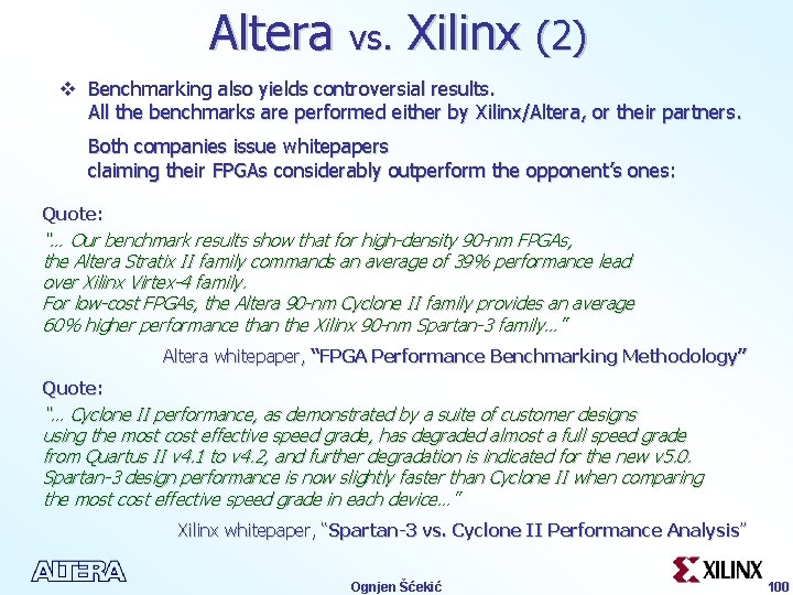
Altera vs. Xilinx (2) v Benchmarking also yields controversial results. All the benchmarks are performed either by Xilinx/Altera, or their partners. Both companies issue whitepapers claiming their FPGAs considerably outperform the opponent’s ones: Quote: “… Our benchmark results show that for high-density 90 -nm FPGAs, the Altera Stratix II family commands an average of 39% performance lead over Xilinx Virtex-4 family. For low-cost FPGAs, the Altera 90 -nm Cyclone II family provides an average 60% higher performance than the Xilinx 90 -nm Spartan-3 family…” Altera whitepaper, “FPGA Performance Benchmarking Methodology” Quote: “… Cyclone II performance, as demonstrated by a suite of customer designs using the most cost effective speed grade, has degraded almost a full speed grade from Quartus II v 4. 1 to v 4. 2, and further degradation is indicated for the new v 5. 0. Spartan-3 design performance is now slightly faster than Cyclone II when comparing the most cost effective speed grade in each device…” Xilinx whitepaper, “Spartan-3 vs. Cyclone II Performance Analysis” Ognjen Šćekić 100

Altera vs. Xilinx (3) Is there. Let a way to find out who is better? us ask the customers: Quote: “… in a survey of more than 350 design teams worldwide, in which respondents were asked to rate their experience with FPGA and EDA companies' products and services, FPGA designers ranked Xilinx highest in reader/customer satisfaction for devices, design tools, service and support, including: Virtex and Spartan FPGAs - "Xilinx continues to lead the pack in performance and features, and goes the extra mile in explaining how to use their devices for particular class of application. " ISE design tools Support staff, and documentation - "Xilinx has made significant improvements to their tool suite over the past year, particularly in the DSP and embedded design areas. " -"Xilinx consistently sets the standard for support staff and resources, particularly with their robust website and responsible and knowledgeable application engineers. " FPGA Journal Ognjen Šćekić 101

Conclusion • It seems that Xilinx is the winner. • But the competition is closing the gaps. • A careful reader will notice that the stated reasons for Xilinx winning the readers’ award have more to do with client relations than with a great difference in performance. • One thing, however, is certain: = A satisfied user vs. Ognjen Šćekić 102

Thank you! The End Ognjen Šćekić 103