Useful Design Guide To Make the PLD Xilinx









![Logic cells Xilinx: The Density Leader ] 40% bigger Logic cells Xilinx: The Density Leader ] 40% bigger](https://slidetodoc.com/presentation_image/99c28ebf1d910ccf8031092f09da6c0e/image-61.jpg)

- Slides: 86

Useful Design Guide To Make the PLD

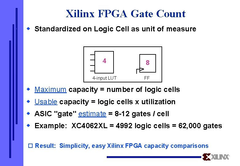
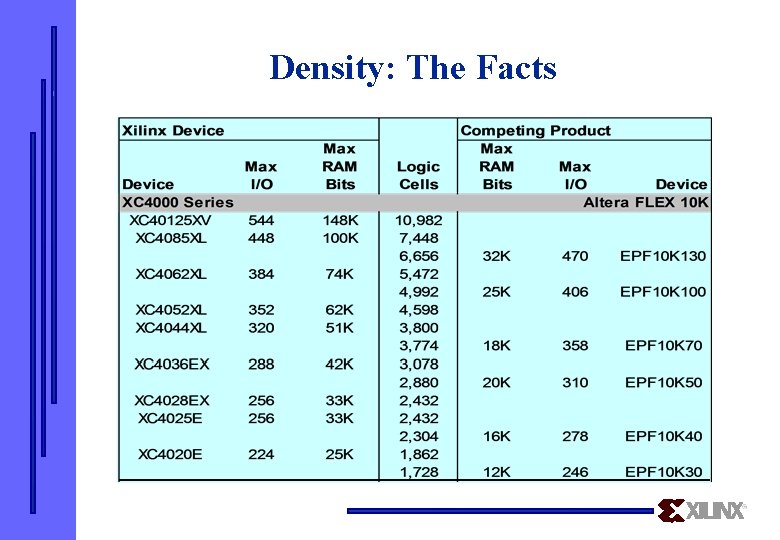
Xilinx FPGA Gate Count w Standardized on Logic Cell as unit of measure 4 8 4 -input LUT FF w Maximum capacity = number of logic cells w Usable capacity = logic cells x utilization w ASIC "gate" estimate = 8 -12 gates / cell w Example: XC 4062 XL = 4992 logic cells = 62, 000 gates o Result: Simplicity, easy Xilinx FPGA capacity comparisons

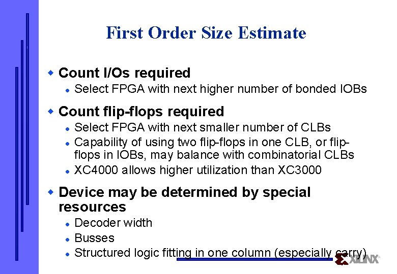
First Order Size Estimate w Count I/Os required l Select FPGA with next higher number of bonded IOBs w Count flip-flops required l l l Select FPGA with next smaller number of CLBs Capability of using two flip-flops in one CLB, or flipflops in IOBs, may balance with combinatorial CLBs XC 4000 allows higher utilization than XC 3000 w Device may be determined by special resources l l l Decoder width Busses Structured logic fitting in one column (especially carry)

Consider Architecture w Use dedicated logic functions w Limit clocks w Abundant flip-flops l Also RAM w AND gate options (e. g. , comparator) l l l Lookup tables Edge decoders Wired-AND of three-state buffers Carry logic Writable RAM

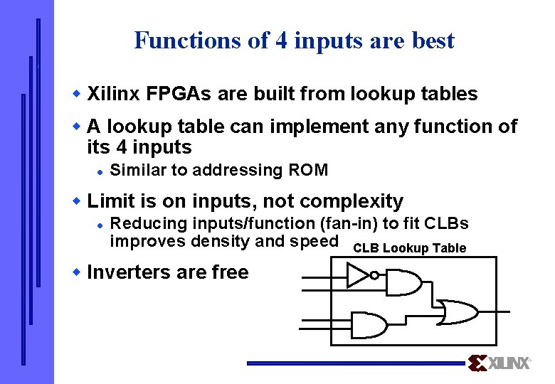
Functions of 4 inputs are best w Xilinx FPGAs are built from lookup tables w A lookup table can implement any function of its 4 inputs l Similar to addressing ROM w Limit is on inputs, not complexity l Reducing inputs/function (fan-in) to fit CLBs improves density and speed CLB Lookup Table w Inverters are free

Why Use to Hierarchy w Adds structure to design w Eases debug w Users can build libraries of common functions w Allows each design portion to be entered by most efficient method w Improves incremental design w Allows for floorplanning w Provides for team design

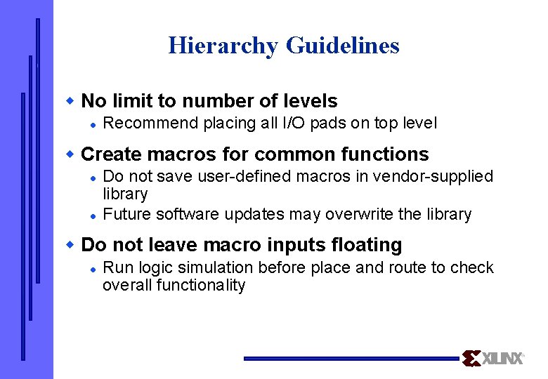
Hierarchy Guidelines w No limit to number of levels l Recommend placing all I/O pads on top level w Create macros for common functions l l Do not save user-defined macros in vendor-supplied library Future software updates may overwrite the library w Do not leave macro inputs floating l Run logic simulation before place and route to check overall functionality

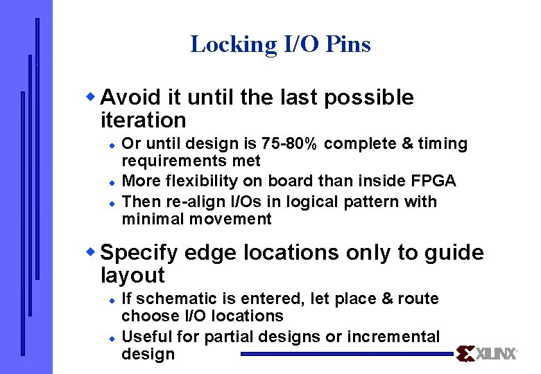
Locking I/O Pins w Avoid it until the last possible iteration l l l Or until design is 75 -80% complete & timing requirements met More flexibility on board than inside FPGA Then re-align I/Os in logical pattern with minimal movement w Specify edge locations only to guide layout l l If schematic is entered, let place & route choose I/O locations Useful for partial designs or incremental design

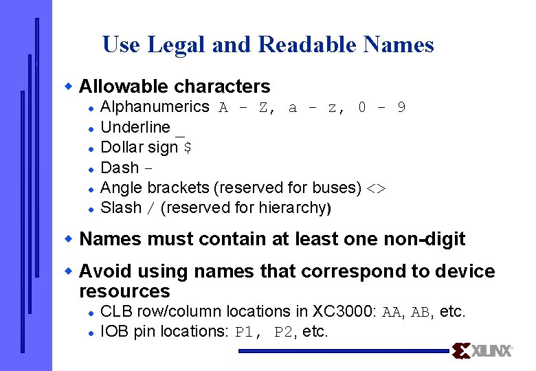
Use Legal and Readable Names w Allowable characters l l l Alphanumerics A - Z, a - z, 0 - 9 Underline _ Dollar sign $ Dash Angle brackets (reserved for buses) <> Slash / (reserved for hierarchy) w Names must contain at least one non-digit w Avoid using names that correspond to device resources l l CLB row/column locations in XC 3000: AA, AB, etc. IOB pin locations: P 1, P 2, etc.

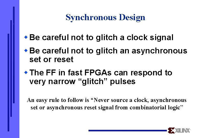
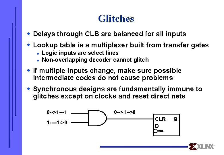
Synchronous Design w Be careful not to glitch a clock signal w Be careful not to glitch an asynchronous set or reset w The FF in fast FPGAs can respond to very narrow “glitch” pulses An easy rule to follow is “Never source a clock, asynchronous set or asynchronous reset signal from combinatorial logic”

Glitches w Delays through CLB are balanced for all inputs w Lookup table is a multiplexer built from transfer gates l l Logic inputs are select lines Non-overlapping decoder cannot glitch w If multiple inputs change, make sure possible intermediate codes do not cause problems w Synchronous designs are fundamentally immune to glitches except on clocks and reset direct nets 0 -->1 ---1 1 ----1 ->0 0 -->1 -->0 CLR D Q

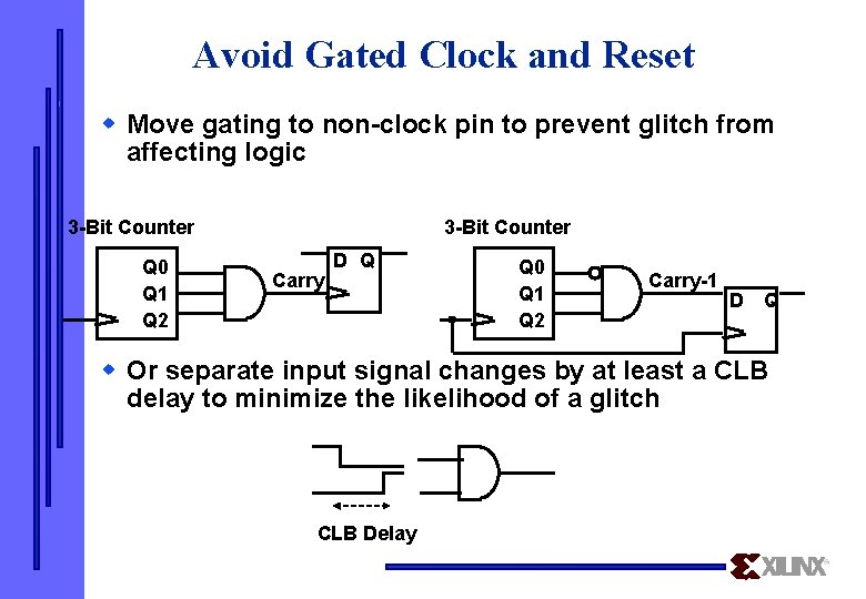
Avoid Gated Clock and Reset w Move gating to non-clock pin to prevent glitch from affecting logic 3 -Bit Counter Q 0 Q 1 Q 2 3 -Bit Counter Carry D Q Q 0 Q 1 Q 2 Carry-1 D Q w Or separate input signal changes by at least a CLB delay to minimize the likelihood of a glitch CLB Delay

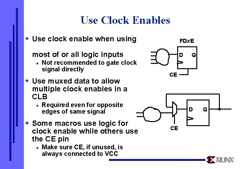
Use Clock Enables w Use clock enable when using FDx. E most of or all logic inputs l Not recommended to gate clock signal directly w Use muxed data to allow multiple clock enables in a CLB l Make sure CE, if unused, is always connected to VCC Q CE Required even for opposite edges of same signal w Some macros use logic for clock enable while others use the CE pin l D D CE Q

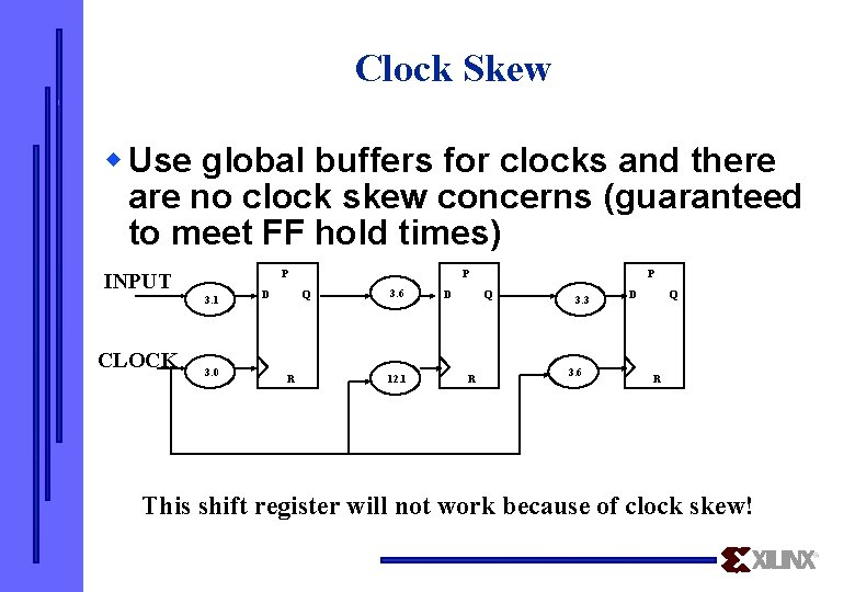
Clock Skew w Use global buffers for clocks and there are no clock skew concerns (guaranteed to meet FF hold times) P INPUT 3. 1 CLOCK 3. 0 D P Q R 3. 6 12. 1 D P Q R 3. 3 3. 6 D Q R This shift register will not work because of clock skew!

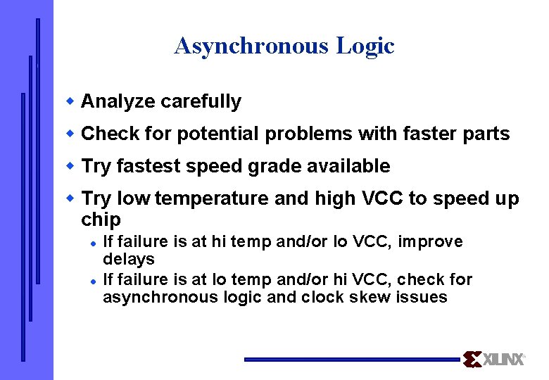
Asynchronous Logic w Analyze carefully w Check for potential problems with faster parts w Try fastest speed grade available w Try low temperature and high VCC to speed up chip l l If failure is at hi temp and/or lo VCC, improve delays If failure is at lo temp and/or hi VCC, check for asynchronous logic and clock skew issues

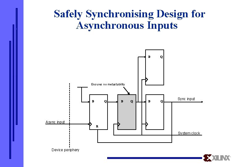
Safely Synchronising Design for Asynchronous Inputs D Q Ensures no metastability D Q Sync input Async input R System clock Device periphery

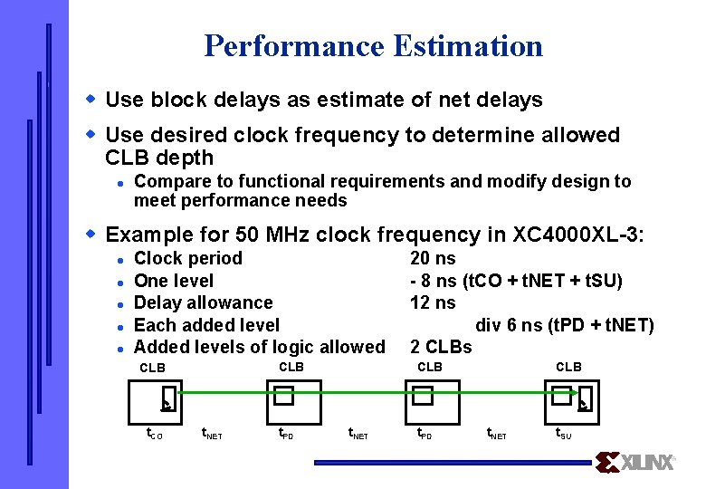
Performance Estimation w Use block delays as estimate of net delays w Use desired clock frequency to determine allowed CLB depth l Compare to functional requirements and modify design to meet performance needs w Example for 50 MHz clock frequency in XC 4000 XL-3: l l l Clock period One level Delay allowance Each added level Added levels of logic allowed CLB t. CO t. NET t. PD 20 ns - 8 ns (t. CO + t. NET + t. SU) 12 ns div 6 ns (t. PD + t. NET) 2 CLBs CLB t. NET t. PD CLB t. NET t. SU

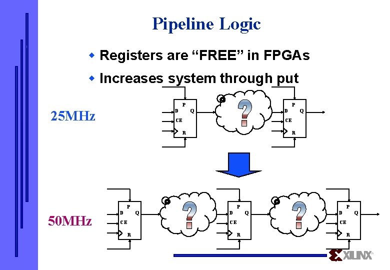
Pipeline Logic w Registers are “FREE” in FPGAs w Increases system through put P 25 MHz D P Q D CE CE R R P 50 MHz D P Q CE R Q D Q CE R R

State Machines Three Types w Binary: The States have a counter like progression S 1 = 001, S 2=010, S 3=011, S 4=100, etc… w Enumerated: The States have assigned values S 1=100, S 2=110, S 3=101, S 4 = 111, etc… w One Hot: Only 1 register is active for each state S 1=00000001, S 2=00000010, S 3=00000100, etc… w Binary and Enumerated have lots of feedback to make the present state to next state jump. This is good for CPLDs like the

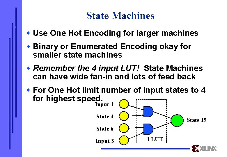
State Machines w Use One Hot Encoding for larger machines w Binary or Enumerated Encoding okay for smaller state machines w Remember the 4 input LUT! State Machines can have wide fan-in and lots of feed back w For One Hot limit number of input states to 4 for highest speed. Input 1 State 4 State 19 State 6 Input 3 1 LUT

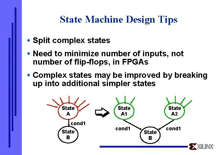
State Machine Design Tips w Split complex states w Need to minimize number of inputs, not number of flip-flops, in FPGAs w Complex states may be improved by breaking up into additional simpler states State A cond 1 State B State A 1 cond 1 State A 2 State B cond 1

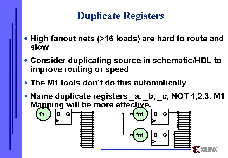
Duplicate Registers w High fanout nets (>16 loads) are hard to route and slow w Consider duplicating source in schematic/HDL to improve routing or speed w The M 1 tools don’t do this automatically w Name duplicate registers _a, _b, _c, NOT 1, 2, 3. M 1 Mapping will be more effective. fn 1 D Q

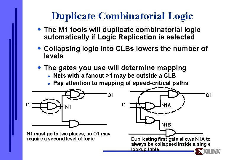
Duplicate Combinatorial Logic w The M 1 tools will duplicate combinatorial logic automatically if Logic Replication is selected w Collapsing logic into CLBs lowers the number of levels w The gates you use will determine mapping l l Nets with a fanout >1 may be outside a CLB Pay attention to mapping of speed-critical paths O 1 I 1 N 1 A N 1 B N 1 must go to two places, so O 1 may require a second level of logic Duplicating first gate allows N 1 A to always be collapsed inside a single lookup table

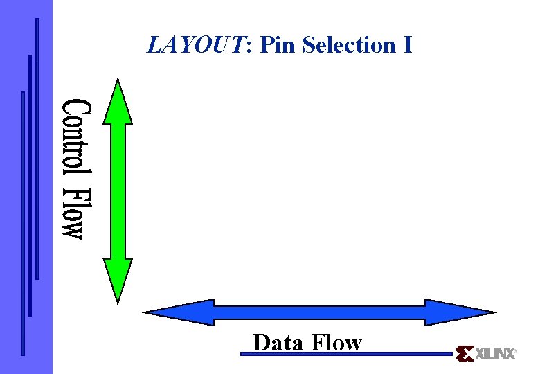
LAYOUT: Pin Selection I Data Flow

LAYOUT: Pin Selection II Control Pins

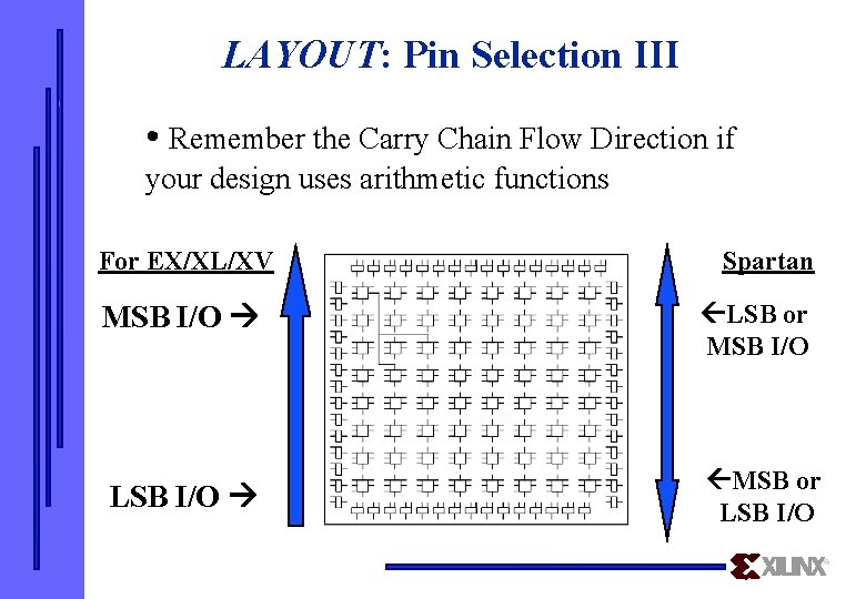
LAYOUT: Pin Selection III • Remember the Carry Chain Flow Direction if your design uses arithmetic functions For EX/XL/XV Spartan MSB I/O LSB or MSB I/O LSB I/O MSB or LSB I/O

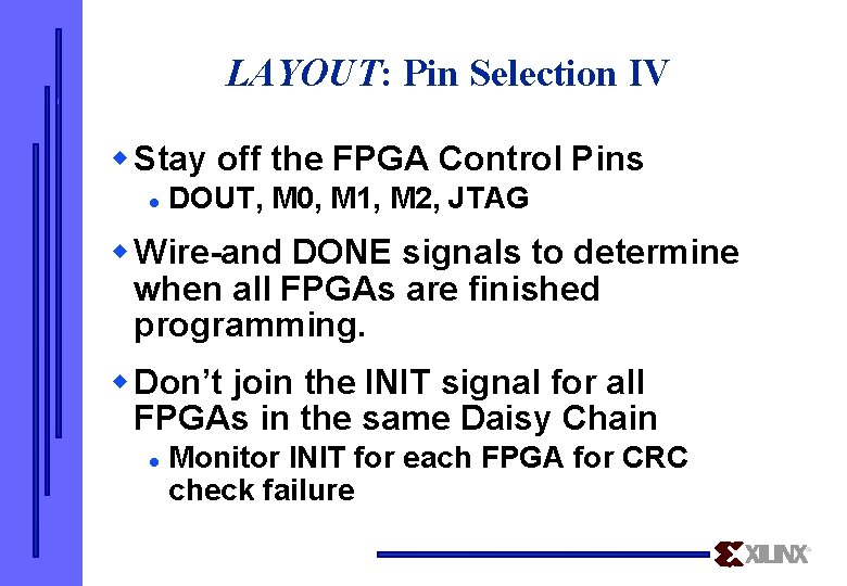
LAYOUT: Pin Selection IV w Stay off the FPGA Control Pins l DOUT, M 0, M 1, M 2, JTAG w Wire-and DONE signals to determine when all FPGAs are finished programming. w Don’t join the INIT signal for all FPGAs in the same Daisy Chain l Monitor INIT for each FPGA for CRC check failure

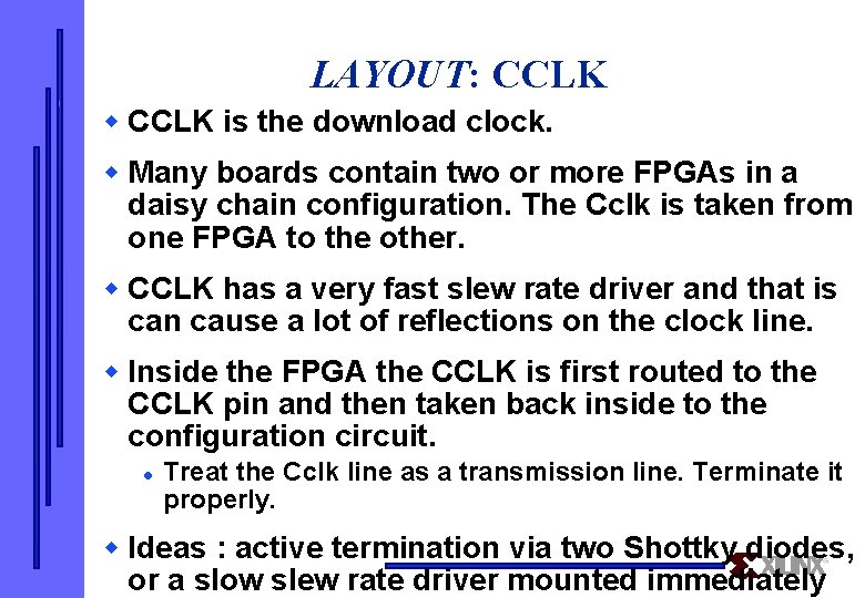
LAYOUT: CCLK w CCLK is the download clock. w Many boards contain two or more FPGAs in a daisy chain configuration. The Cclk is taken from one FPGA to the other. w CCLK has a very fast slew rate driver and that is can cause a lot of reflections on the clock line. w Inside the FPGA the CCLK is first routed to the CCLK pin and then taken back inside to the configuration circuit. l Treat the Cclk line as a transmission line. Terminate it properly. w Ideas : active termination via two Shottky diodes, or a slow slew rate driver mounted immediately

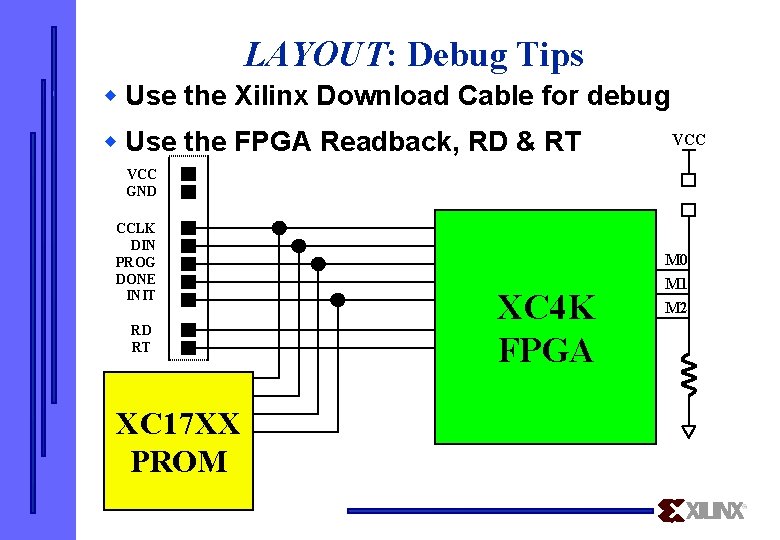
LAYOUT: Debug Tips Use Tick marks To help with pin identification on your board

LAYOUT: Debug Tips w Use the Xilinx Download Cable for debug w Use the FPGA Readback, RD & RT VCC GND CCLK DIN PROG DONE INIT RD RT XC 17 XX PROM M 0 XC 4 K FPGA M 1 M 2

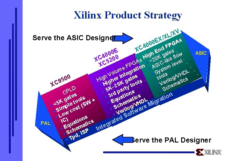
Xilinx Product Strategy Serve the ASIC Designer V X E 0 00 /X L /X As G FP 4 C d X E En ates 0 ASIC h 0 w g 0 g i o l 4 H K ke f 0 XC 5200 2 s A w > IC-li evel C G X FP tion w AS tem l e ys lum tegra S DL o s w H V l 0 too ilog/V ics igh her in ates 0 H 5 9 er mat ig 0 K g ools V H XC w che w K– 2 ty t D r L w. S w 5 rd pa ns CP s n 3 tio tics e ls o t i a w t a u g too + Eq ema HDL igra K 5 W w e ch og/V re M w < impl st (S S w eril wa w S ow co V oft w L S s w ) d n e o C t i I PAL uat atics tegra q w E chem P In w S pd, IS w. T Serve the PAL Designer


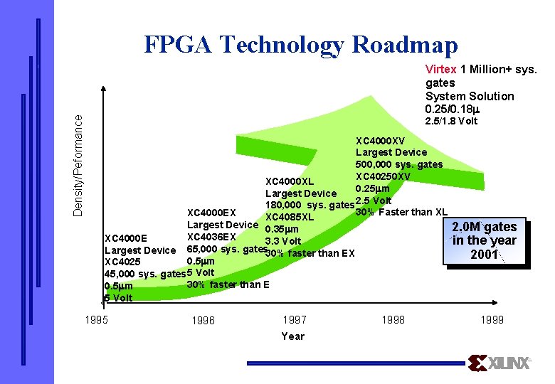
Density/Peformance FPGA Technology Roadmap Virtex 1 Million+ sys. gates System Solution 0. 25/0. 18 2. 5/1. 8 Volt XC 4000 XV Largest Device 500, 000 sys. gates XC 40250 XV XC 4000 XL 0. 25 m Largest Device 180, 000 sys. gates 2. 5 Volt 30% Faster than XL XC 4085 XL XC 4000 EX Largest Device 0. 35 m XC 4036 EX XC 4000 E 3. 3 Volt 65, 000 sys. gates Largest Device 30% faster than EX 0. 5 m XC 4025 45, 000 sys. gates 5 Volt 30% faster than E 0. 5 m 5 Volt 1995 1996 1997 Year 1998 2. 0 M gates in the year 2001 1999

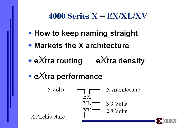
4000 Series X = EX/XL/XV w How to keep naming straight w Markets the X architecture w e. Xtra routing e. Xtra density w e. Xtra performance 5 Volts X Architecture EX XL XV 3. 3 Volts 2. 5 Volts

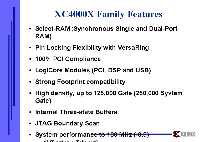
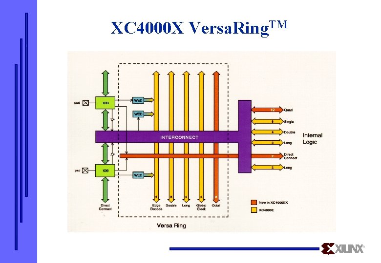
XC 4000 X Family Features • Select-RAM (Synchronous Single and Dual-Port RAM) • Pin Locking Flexibility with Versa. Ring • 100% PCI Compliance • Logi. Core Modules (PCI, DSP and USB) • Strong Footprint compatibility • High density, up to 125, 000 Gate (250, 000 System Gate) • Internal Three-state Buffers • JTAG Boundary Scan • System performance to 100 MHz (-0. 9)

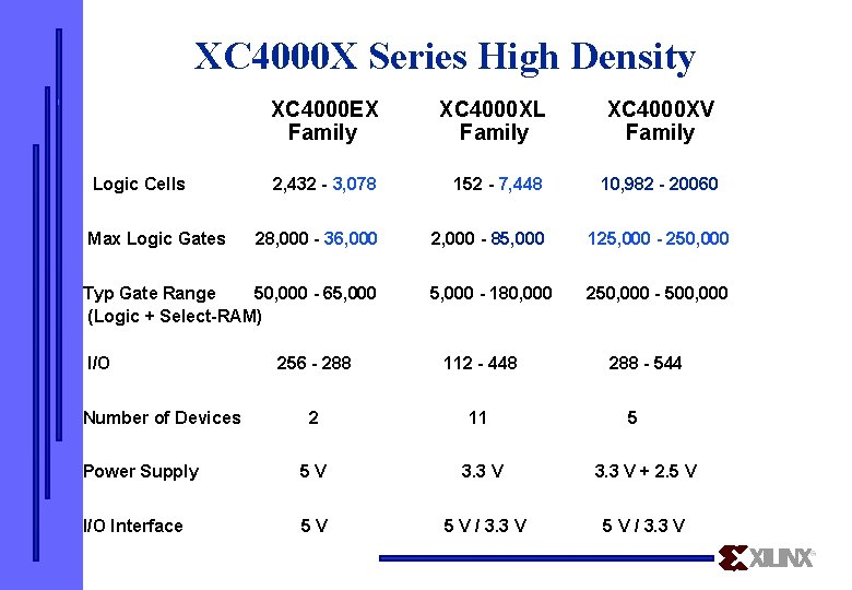
XC 4000 X Series High Density Logic Cells Max Logic Gates XC 4000 EX Family XC 4000 XL Family XC 4000 XV Family 2, 432 - 3, 078 152 - 7, 448 10, 982 - 20060 28, 000 - 36, 000 2, 000 - 85, 000 125, 000 - 250, 000 5, 000 - 180, 000 250, 000 - 500, 000 Typ Gate Range 50, 000 - 65, 000 (Logic + Select-RAM) I/O 256 - 288 112 - 448 2 11 Power Supply 5 V 3. 3 V + 2. 5 V I/O Interface 5 V 5 V / 3. 3 V Number of Devices 288 - 544 5

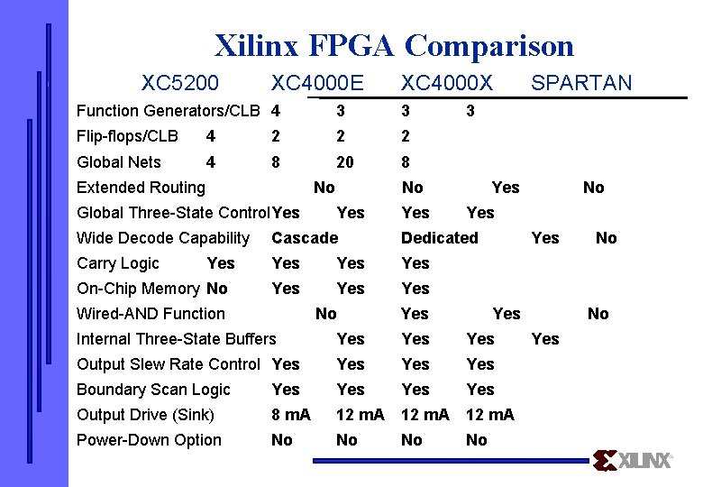
Xilinx FPGA Comparison XC 5200 XC 4000 E XC 4000 X Function Generators/CLB 4 3 3 Flip-flops/CLB 4 2 2 2 Global Nets 4 8 20 8 Extended Routing No Global Three-State Control. Yes 3 No Yes Yes Cascade Dedicated Carry Logic Yes Yes Yes On-Chip Memory No Wired-AND Function No Yes Yes Internal Three-State Buffers Yes Yes Output Slew Rate Control Yes Yes Boundary Scan Logic Yes Yes Output Drive (Sink) 8 m. A 12 m. A Power-Down Option No No Yes Wide Decode Capability Yes SPARTAN No No No Yes

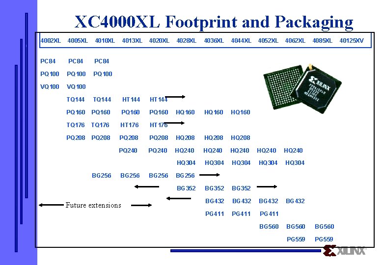
XC 4000 XL Footprint and Packaging 4002 XL 4005 XL 4010 XL PC 84 PQ 100 VQ 100 4013 XL 4020 XL 4028 XL 4036 XL 4044 XL HQ 160 4052 XL 4062 XL TQ 144 HT 144 PQ 160 TQ 176 HT 176 PQ 208 HQ 208 PQ 240 HQ 240 HQ 304 HQ 304 BG 352 BG 432 PG 411 BG 256 BG 352 Future extensions 4085 XL BG 560 PG 559 40125 XV

Density: The Facts


XC 4000 Series FPGA Architecture

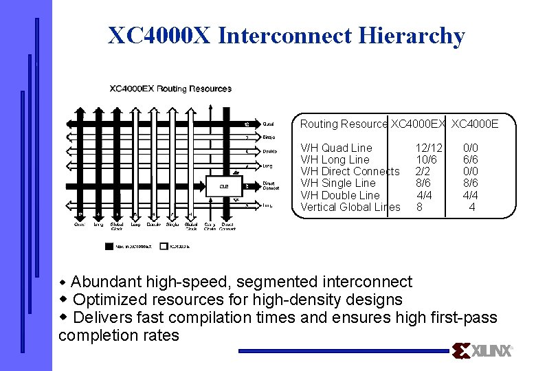
XC 4000 X Interconnect Hierarchy Routing Resource XC 4000 EX XC 4000 E V/H Quad Line V/H Long Line V/H Direct Connects V/H Single Line V/H Double Line Vertical Global Lines w Abundant high-speed, segmented interconnect 12/12 10/6 2/2 8/6 4/4 8 0/0 6/6 0/0 8/6 4/4 4 w Optimized resources for high-density designs w Delivers fast compilation times and ensures high first-pass completion rates

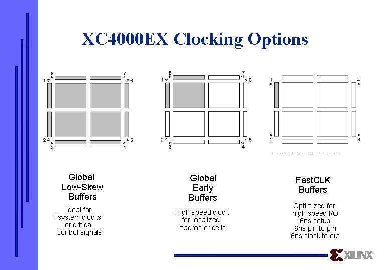
XC 4000 EX Clocking Options Global Low-Skew Buffers Ideal for “system clocks” or critical control signals Global Early Buffers High speed clock for localized macros or cells Fast. CLK Buffers Optimized for high-speed I/O 6 ns setup 6 ns pin to pin 6 ns clock to out

XC 4000 X Versa. Ring. TM

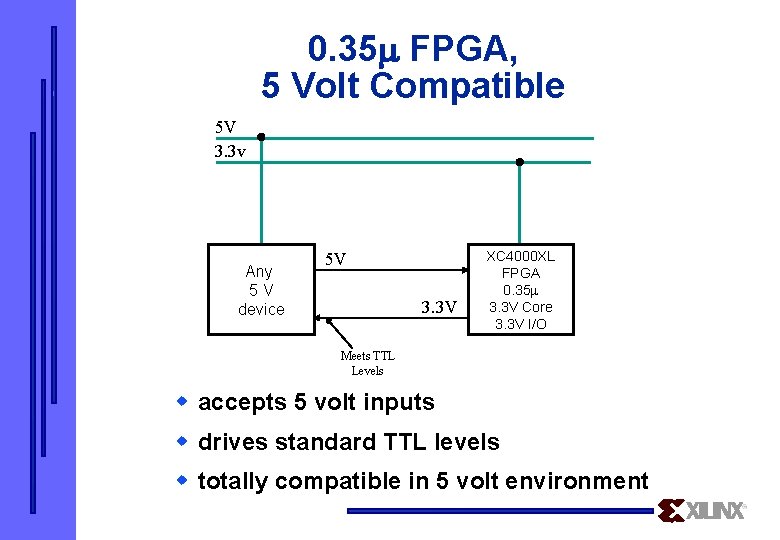
0. 35 FPGA, 5 Volt Compatible 5 V 3. 3 v Any 5 V device 5 V 3. 3 V XC 4000 XL FPGA 0. 35 3. 3 V Core 3. 3 V I/O Meets TTL Levels w accepts 5 volt inputs w drives standard TTL levels w totally compatible in 5 volt environment

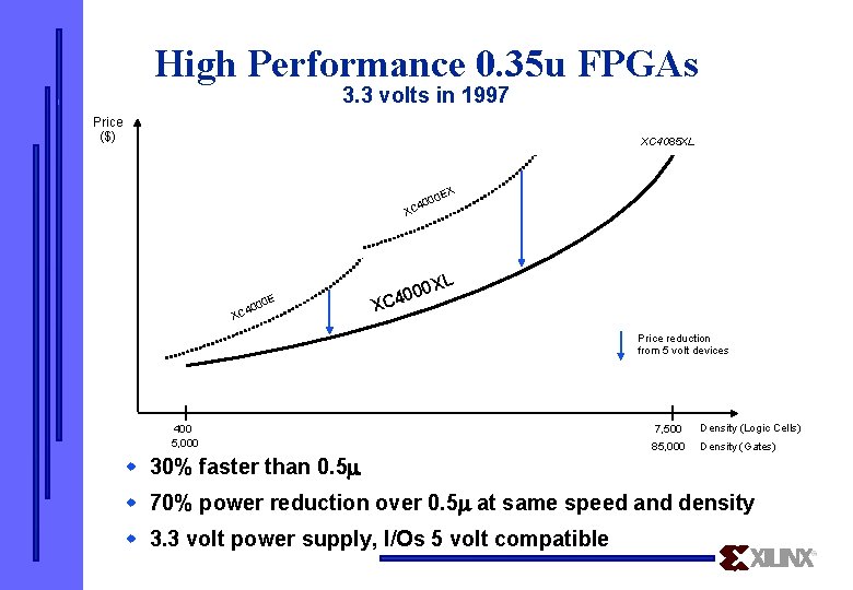
High Performance 0. 35 u FPGAs 3. 3 volts in 1997 Price ($) XC 4085 XL X 0 E 00 C 4 X E 000 4 XC 0 XL 0 0 C 4 X Price reduction from 5 volt devices 400 5, 000 7, 500 Density (Logic Cells) 85, 000 Density (Gates) w 30% faster than 0. 5 w 70% power reduction over 0. 5 at same speed and density w 3. 3 volt power supply, I/Os 5 volt compatible

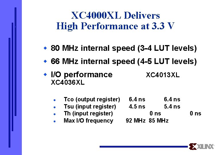
XC 4000 XL Delivers High Performance at 3. 3 V w 80 MHz internal speed (3 -4 LUT levels) w 66 MHz internal speed (4 -5 LUT levels) w I/O performance XC 4013 XL XC 4036 XL l l Tco (output register) Tsu (input register) Th (input register) Max I/O frequency 6. 4 ns 4. 5 ns 6. 4 ns 5. 4 ns 0 ns 92 MHz 85 MHz 0 ns

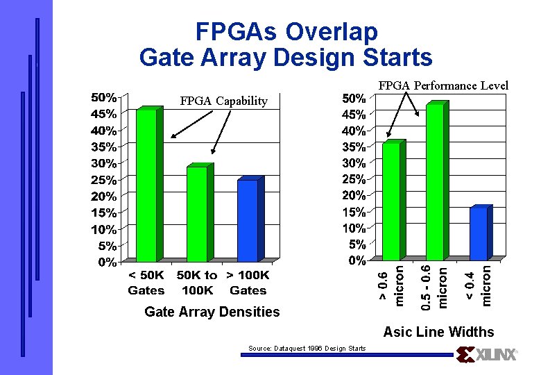
FPGAs Overlap Gate Array Design Starts FPGA Performance Level FPGA Capability Gate Array Densities Asic Line Widths Source: Dataquest 1996 Design Starts

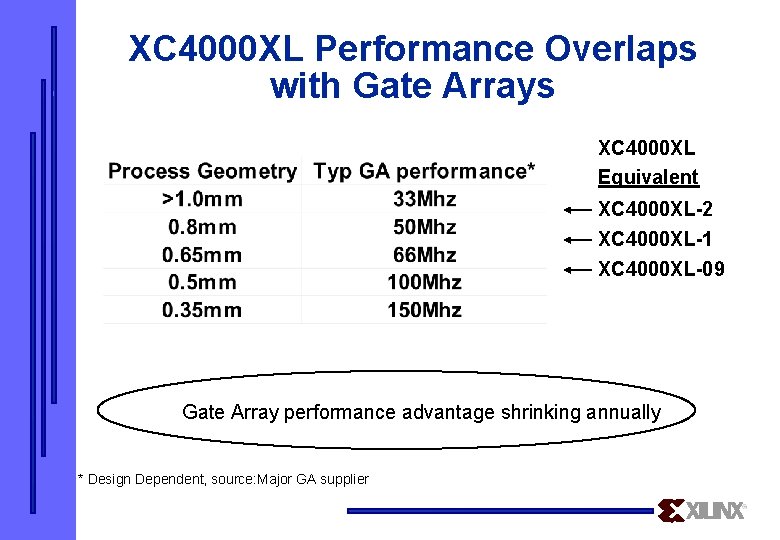
XC 4000 XL Performance Overlaps with Gate Arrays XC 4000 XL Equivalent XC 4000 XL-2 XC 4000 XL-1 XC 4000 XL-09 Gate Array performance advantage shrinking annually * Design Dependent, source: Major GA supplier

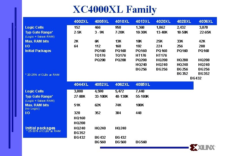
XC 4000 XL Family 4002 XL 4005 XL 4010 XL 4013 XL 4020 XL 4028 XL 4036 XL 152 2 -5 K 466 3 - 9 K 950 7 -20 K 1, 368 10 -30 K 1, 862 13 -40 K 2, 432 18 -50 K 3, 078 22 -65 K 2 K 64 6 K 112 PQ 160 TQ 176 PQ 208 13 K 160 PQ 160 TQ 176 PQ 208 18 K 192 PQ 160 HT 176 PQ 208 HQ 240 BG 256 25 K 224 PQ 160 HT 176 HQ 208 HQ 240 BG 256 33 K 256 PQ 160 42 K 288 PQ 160 HQ 208 HQ 240 BG 256 BG 352 BG 432 4044 XL 4052 XL 4062 XL 4085 XL 3, 800 27 -80 K 4, 598 33 -100 K 5, 472 40 -130 K 7, 448 55 -180 K Max. RAM bits 51 K 62 K 74 K 100 K I/O 320 HQ 160 HQ 208 352 384 448 Initial packages HQ 240 BG 352 BG 432 HQ 240 BG 432 BG 560 Logic Cells Typ Gate Range* (Logic + Select-RAM) Max. RAM bits I/O Initial Packages * 20 -25% of CLBs as RAM Logic Cells Typ Gate Range* (Logic + Select-RAM) (no Logic) * 25 -30% of CLBs as RAM BG 560

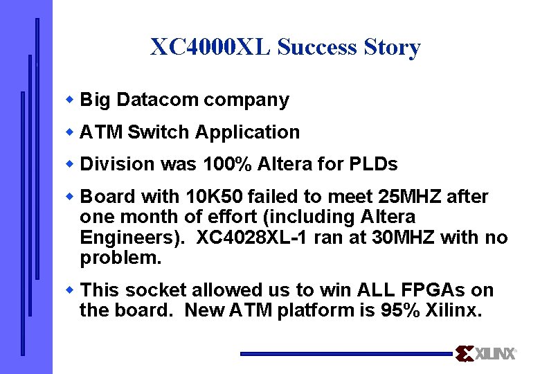
XC 4000 XL Success Story w Big Datacom company w ATM Switch Application w Division was 100% Altera for PLDs w Board with 10 K 50 failed to meet 25 MHZ after one month of effort (including Altera Engineers). XC 4028 XL-1 ran at 30 MHZ with no problem. w This socket allowed us to win ALL FPGAs on the board. New ATM platform is 95% Xilinx.

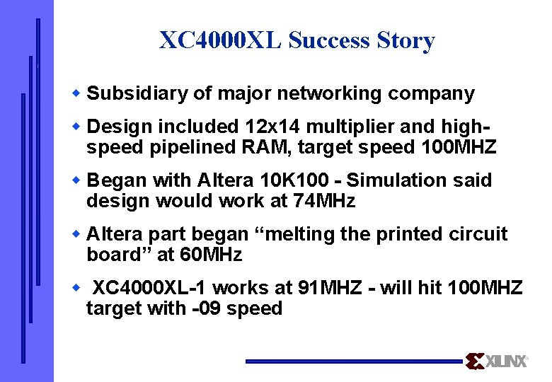
XC 4000 XL Success Story w Subsidiary of major networking company w Design included 12 x 14 multiplier and highspeed pipelined RAM, target speed 100 MHZ w Began with Altera 10 K 100 - Simulation said design would work at 74 MHz w Altera part began “melting the printed circuit board” at 60 MHz w XC 4000 XL-1 works at 91 MHZ - will hit 100 MHZ target with -09 speed

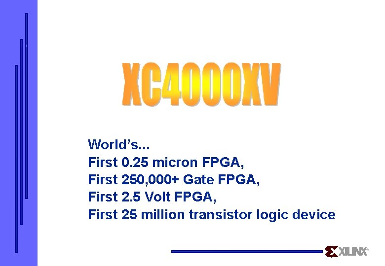
World’s. . . First 0. 25 micron FPGA, First 250, 000+ Gate FPGA, First 2. 5 Volt FPGA, First 25 million transistor logic device

Technology Leadership: XC 4000 XV Family w Advanced process technology 5 layer metal l 0. 25 u CMOS l stacked vias l CMP (chemical mechanical polishing) l w XC 4000 XV+ includes extra routing 100 XV, 150 XV, 200 XV, 250 XV l eight tracks of octal lines added per CLB l minimizes routing congestion l

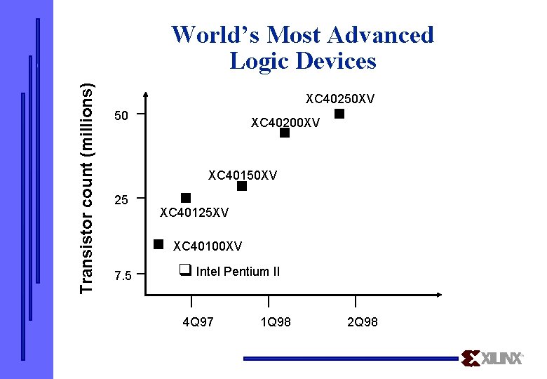
Transistor count (millions) World’s Most Advanced Logic Devices XC 40250 XV 50 XC 40200 XV XC 40150 XV 25 XC 40125 XV 7. 5 XC 40100 XV Intel Pentium II 4 Q 97 1 Q 98 2 Q 98

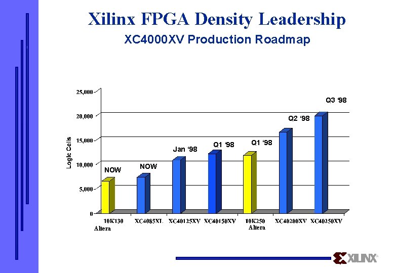
Xilinx FPGA Density Leadership XC 4000 XV Production Roadmap Q 3 ‘ 98 Q 2 ‘ 98 Jan ‘ 98 NOW Altera Q 1 ‘ 98 NOW Altera

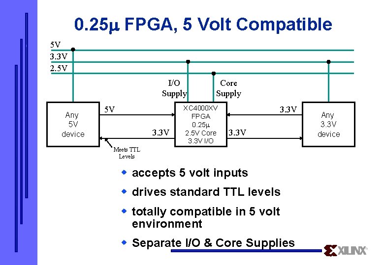
0. 25 FPGA, 5 Volt Compatible 5 V 3. 3 V 2. 5 V I/O Supply Any 5 V device 5 V 3. 3 V Core Supply XC 4000 XV FPGA 0. 25 2. 5 V Core 3. 3 V I/O 3. 3 V Meets TTL Levels w accepts 5 volt inputs w drives standard TTL levels w totally compatible in 5 volt environment w Separate I/O & Core Supplies Any 3. 3 V device

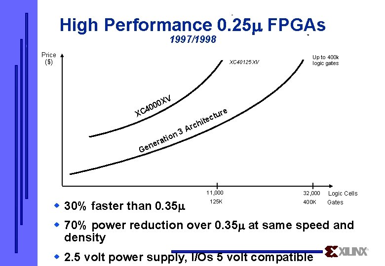
High Performance 0. 25 FPGAs 1997/1998 Price ($) XC 40125 XV Up to 400 k logic gates V X 000 4 XC ure t c ite h ion t a er rc 3 A n Ge 11, 000 w 30% faster than 0. 35 125 K 32, 000 400 K Logic Cells Gates w 70% power reduction over 0. 35 at same speed and density w 2. 5 volt power supply, I/Os 5 volt compatible

The XC 4000 XV - 0. 25 µm Fast w Performance summary XC 40125 XV Internal operation (3 -4 LUT levels) 100 MHz l Tco (output register) 7. 5 ns l Tsu (input register) 5. 0 ns l Max I/O frequency 80 MHz l w XC 40125 XV: 10, 982 logic cells (265, 000 system gates) Combining VERY high density AND VERY high performance

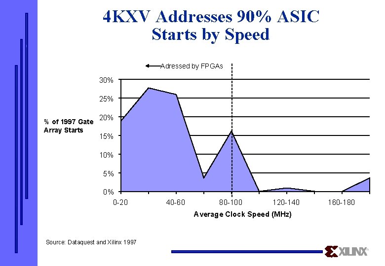
4 KXV Addresses 90% ASIC Starts by Speed Adressed by FPGAs 30% 25% % of 1997 Gate Array Starts 20% 15% 10% 5% 0% 0 -20 40 -60 80 -100 120 -140 Average Clock Speed (MHz) Source: Dataquest and Xilinx 1997 160 -180
![Logic cells Xilinx The Density Leader 40 bigger Logic cells Xilinx: The Density Leader ] 40% bigger](https://slidetodoc.com/presentation_image/99c28ebf1d910ccf8031092f09da6c0e/image-61.jpg)
Logic cells Xilinx: The Density Leader ] 40% bigger

XC 4000 XV Family

Foundation FPGA Express

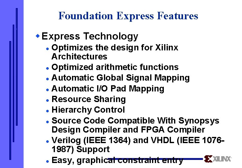
Foundation Express Features w Express Technology Optimizes the design for Xilinx Architectures l Optimized arithmetic functions l Automatic Global Signal Mapping l Automatic I/O Pad Mapping l Resource Sharing l Hierarchy Control l Source Code Compatible With Synopsys Design Compiler and FPGA Compiler l Verilog (IEEE 1364) and VHDL (IEEE 10761987) Support l Easy, graphical constraint entry l

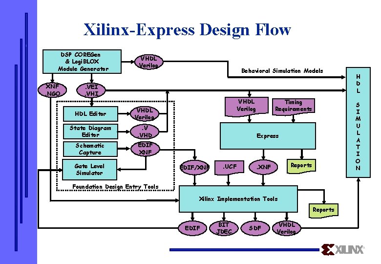
Xilinx-Express Design Flow DSP COREGen & Logi. BLOX Module Generator XNF. NGO VHDL Verilog Behavioral Simulation Models . VEI. VHI HDL Editor VHDL Verilog State Diagram Editor . V. VHD Schematic Capture EDIF XNF Gate Level Simulator VHDL Verilog Timing Requirements S I M U L A T I O N Express EDIF/XNF . UCF Reports . XNF Foundation Design Entry Tools Xilinx Implementation Tools Reports EDIF BIT JDEC SDF VHDL Verilog H D L

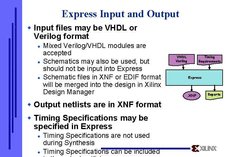
Express Input and Output w Input files may be VHDL or Verilog format l l l Mixed Verilog/VHDL modules are accepted Schematics may also be used, but should not be input into Express Schematic files in XNF or EDIF format will be merged into the design in Xilinx Design Manager w Output netlists are in XNF format w Timing Specifications may be specified in Express l l Timing Specifications are not used during Synthesis Timing Specifications can be included VHDL Verilog Timing Requirements Express . XNF Reports

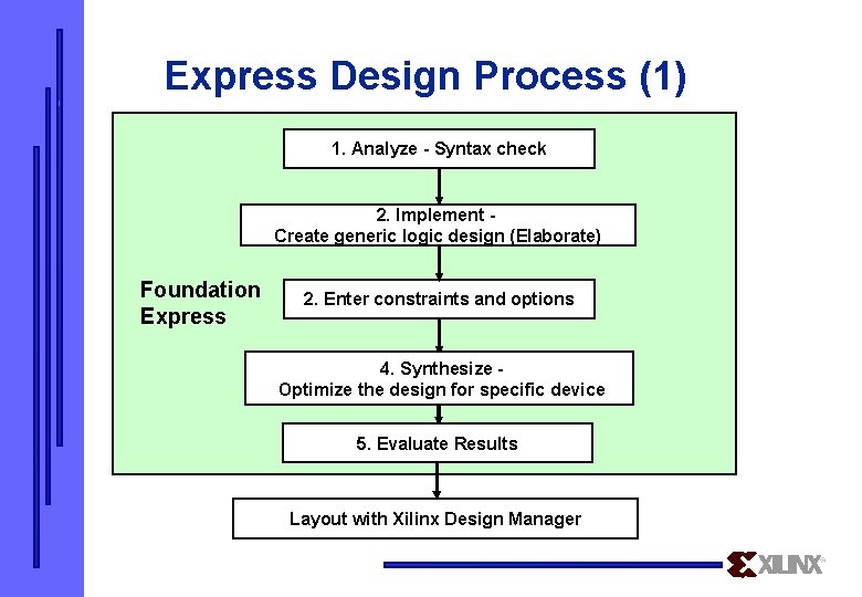
Express Design Process (1) 1. Analyze - Syntax check 2. Implement Create generic logic design (Elaborate) Foundation Express 2. Enter constraints and options 4. Synthesize Optimize the design for specific device 5. Evaluate Results Layout with Xilinx Design Manager

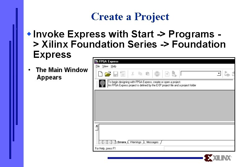
Create a Project w Invoke Express with Start -> Programs > Xilinx Foundation Series -> Foundation Express • The Main Window Appears

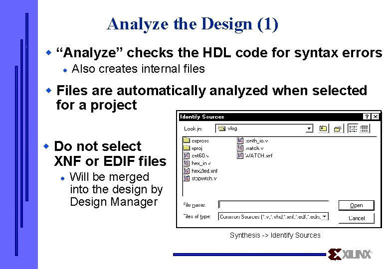
Analyze the Design (1) w “Analyze” checks the HDL code for syntax errors l Also creates internal files w Files are automatically analyzed when selected for a project w Do not select XNF or EDIF files l Will be merged into the design by Design Manager Synthesis -> Identify Sources

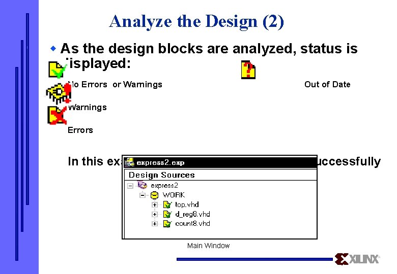
Analyze the Design (2) w As the design blocks are analyzed, status is displayed: No Errors or Warnings Out of Date Warnings Errors In this example, all blocks were analyzed successfully Main Window

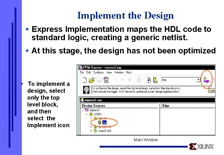
Implement the Design w Express Implementation maps the HDL code to standard logic, creating a generic netlist. w At this stage, the design has not been optimized • To implement a design, select only the top level block, and then select the Implement icon Main Window

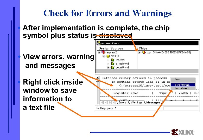
Check for Errors and Warnings w After implementation is complete, the chip symbol plus status is displayed w View errors, warnings and messages w Right click inside window to save information to a text file

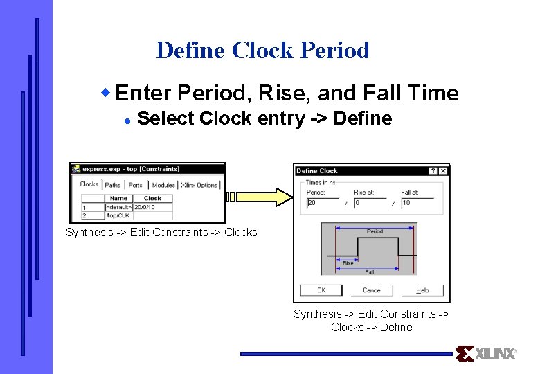
Define Clock Period w Enter Period, Rise, and Fall Time l Select Clock entry -> Define Synthesis -> Edit Constraints -> Clocks -> Define

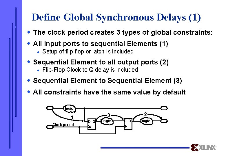
Define Global Synchronous Delays (1) w The clock period creates 3 types of global constraints: w All input ports to sequential Elements (1) l Setup of flip-flop or latch is included w Sequential Element to all output ports (2) l Flip-Flop Clock to Q delay is included w Sequential Element to Sequential Element (3) w All constraints have the same value by default logic 1 Clock period 2 3 D Q logic

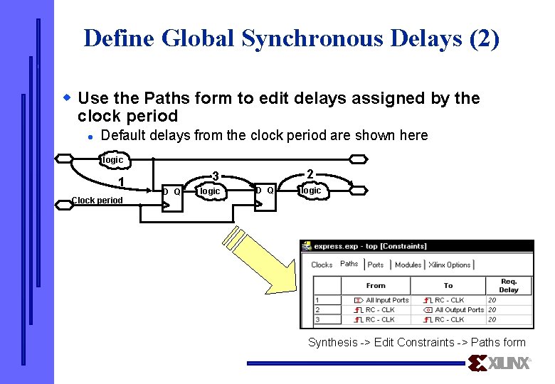
Define Global Synchronous Delays (2) w Use the Paths form to edit delays assigned by the clock period l Default delays from the clock period are shown here logic 1 Clock period 2 3 D Q logic Synthesis -> Edit Constraints -> Paths form

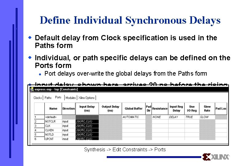
Define Individual Synchronous Delays w Default delay from Clock specification is used in the Paths form w Individual, or path specific delays can be defined on the Ports form l Port delays over-write the global delays from the Paths form w Input delay, shown here, arrives 20 ns before the rising edge of the clock. Synthesis -> Edit Constraints -> Ports

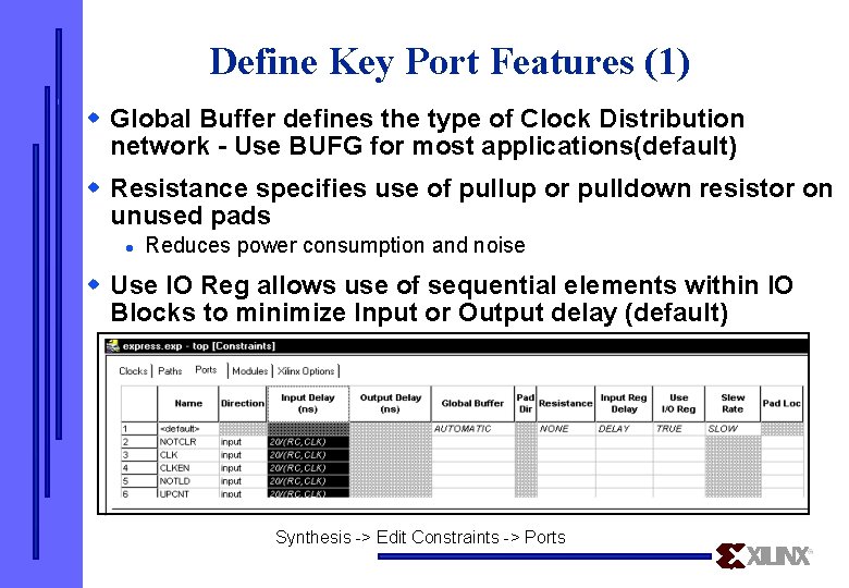
Define Key Port Features (1) w Global Buffer defines the type of Clock Distribution network - Use BUFG for most applications(default) w Resistance specifies use of pullup or pulldown resistor on unused pads l Reduces power consumption and noise w Use IO Reg allows use of sequential elements within IO Blocks to minimize Input or Output delay (default) l Dependent on device type Synthesis -> Edit Constraints -> Ports

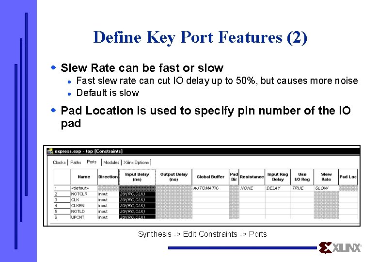
Define Key Port Features (2) w Slew Rate can be fast or slow l l Fast slew rate can cut IO delay up to 50%, but causes more noise Default is slow w Pad Location is used to specify pin number of the IO pad Synthesis -> Edit Constraints -> Ports

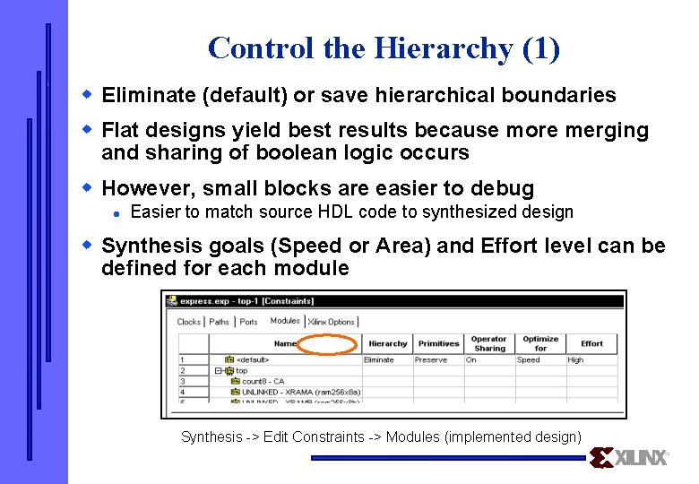
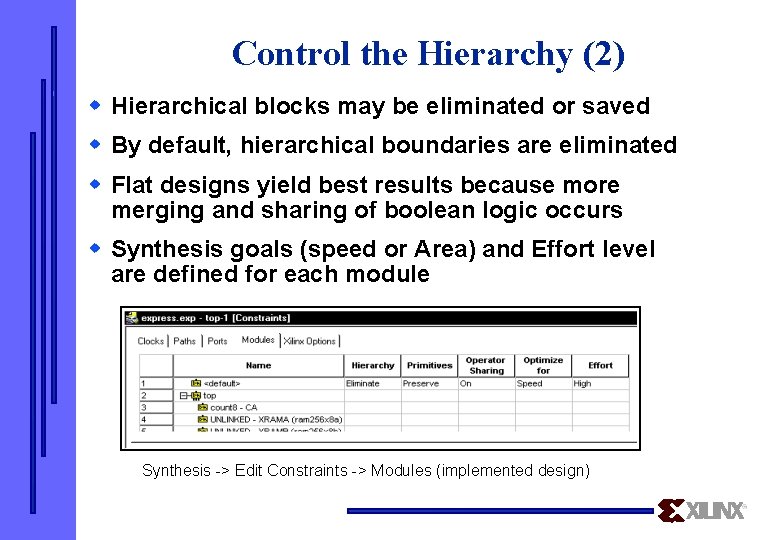
Control the Hierarchy (1) w Eliminate (default) or save hierarchical boundaries w Flat designs yield best results because more merging and sharing of boolean logic occurs w However, small blocks are easier to debug l Easier to match source HDL code to synthesized design w Synthesis goals (Speed or Area) and Effort level can be defined for each module Synthesis -> Edit Constraints -> Modules (implemented design)

Control the Hierarchy (2) w Hierarchical blocks may be eliminated or saved w By default, hierarchical boundaries are eliminated w Flat designs yield best results because more merging and sharing of boolean logic occurs w Synthesis goals (speed or Area) and Effort level are defined for each module Synthesis -> Edit Constraints -> Modules (implemented design)

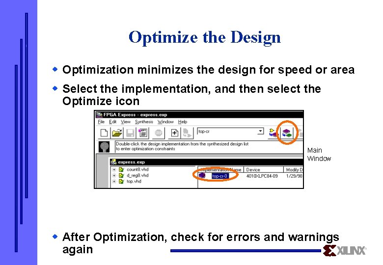
Optimize the Design w Optimization minimizes the design for speed or area w Select the implementation, and then select the Optimize icon Main Window w After Optimization, check for errors and warnings again

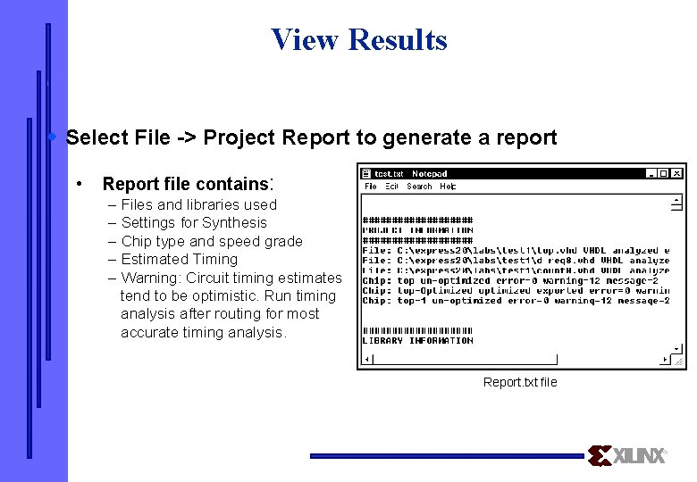
View Results w Select File -> Project Report to generate a report • Report file contains: – Files and libraries used – Settings for Synthesis – Chip type and speed grade – Estimated Timing – Warning: Circuit timing estimates tend to be optimistic. Run timing analysis after routing for most accurate timing analysis. Report. txt file

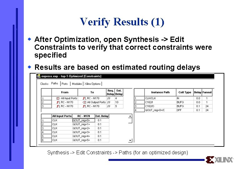
Verify Results (1) w After Optimization, open Synthesis -> Edit Constraints to verify that correct constraints were specified w Results are based on estimated routing delays Synthesis -> Edit Constraints -> Paths (for an optimized design)

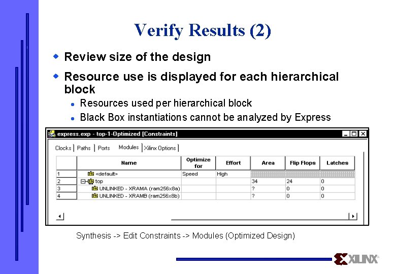
Verify Results (2) w Review size of the design w Resource use is displayed for each hierarchical block l l Resources used per hierarchical block Black Box instantiations cannot be analyzed by Express Synthesis -> Edit Constraints -> Modules (Optimized Design)

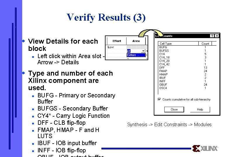
Verify Results (3) w View Details for each block l Left click within Area slot --> Arrow -> Details w Type and number of each Xilinx component are used. l l l l BUFG - Primary or Secondary Buffer BUFGS - Secondary Buffer CY 4* - Carry Logic Function DFF - CLB flip-flop FMAP, HMAP - F and H LUTS IBUF - IOB input buffer INFF - IOB flip-flop Synthesis -> Edit Constraints -> Modules

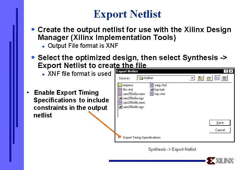
Export Netlist w Create the output netlist for use with the Xilinx Design Manager (Xilinx Implementation Tools) l Output File format is XNF w Select the optimized design, then select Synthesis -> Export Netlist to create the file l XNF file format is used • Enable Export Timing Specifications to include constraints in the output netlist Synthesis -> Export Netlist