
CSNSM ECAL Electronics Status 26112020 ASIC design SKIROC
- Slides: 17
CSNSM ECAL Electronics Status 26/11/2020
ASIC design SKIROC 2 26/11/2020 ECAL electronics - Orsay, 1/12/08 2
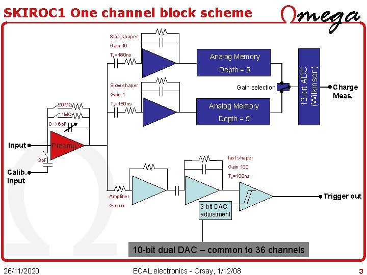
SKIROC 1 One channel block scheme Slow shaper Gain 10 Tp=180 ns Depth = 5 Slow shaper Gain selection Gain 1 20 MΩ Tp=180 ns 1 MΩ Charge Meas. Depth = 5 0 6 p. F Input Analog Memory 12 -bit ADC (Wilkinson) Analog Memory Preamp. fast shaper 3 p. F Gain 100 Calib. Input Tp=100 ns Trigger out Amplifier Gain 5 3 -bit DAC adjustment 10 -bit dual DAC – common to 36 channels 26/11/2020 ECAL electronics - Orsay, 1/12/08 3
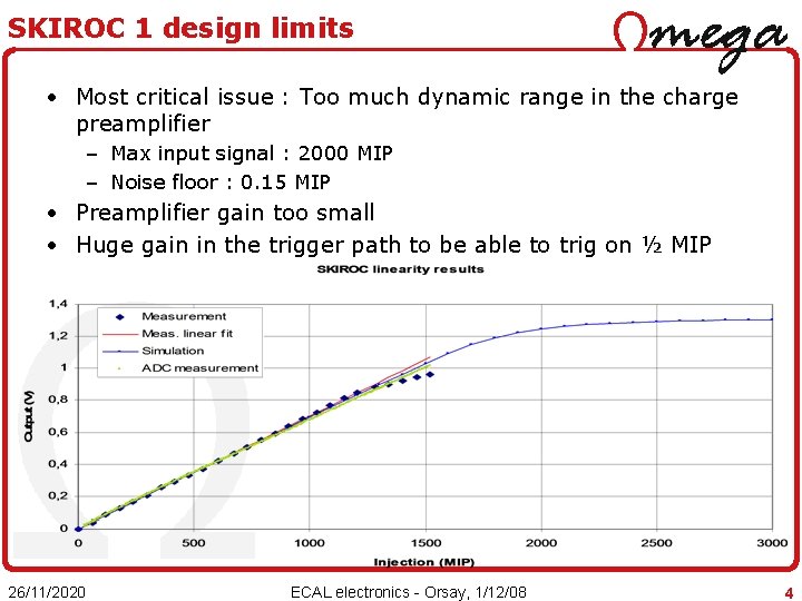
SKIROC 1 design limits • Most critical issue : Too much dynamic range in the charge preamplifier – Max input signal : 2000 MIP – Noise floor : 0. 15 MIP • Preamplifier gain too small • Huge gain in the trigger path to be able to trig on ½ MIP 26/11/2020 ECAL electronics - Orsay, 1/12/08 4
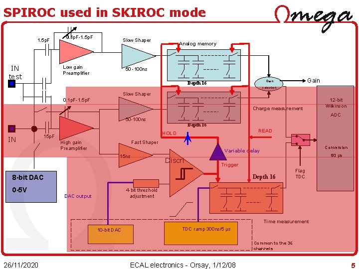
SPIROC used in SKIROC mode 1. 5 p. F IN test 0. 1 p. F-1. 5 p. F Slow Shaper Low gain Preamplifier Analog memory 50 -100 ns Gain Depth 16 selection Slow Shaper 0. 1 p. F-1. 5 p. F Charge measurement 12 -bit Wilkinson ADC 50 -100 ns Depth 16 IN READ HOLD 15 p. F High gain Preamplifier Fast Shaper 15 ns Discri 80 µs Trigger Depth 16 8 -bit DAC 0 -5 V Conversion Variable delay Flag TDC 4 -bit threshold adjustment DAC output Time measurement 10 -bit DAC TDC ramp 300 ns/5 µs Common to the 36 channels 26/11/2020 ECAL electronics - Orsay, 1/12/08 5
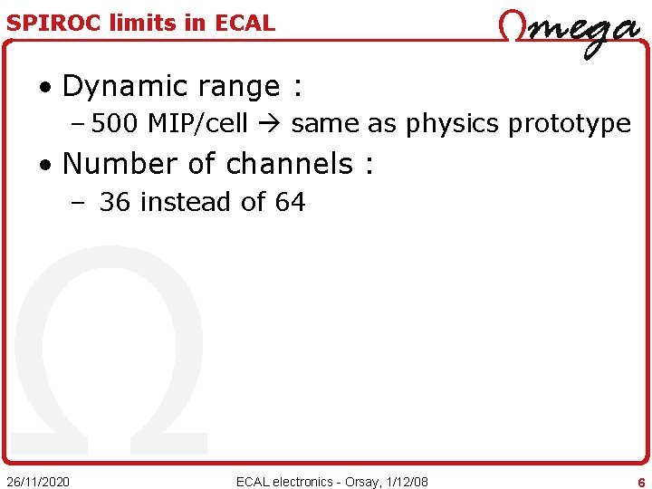
SPIROC limits in ECAL • Dynamic range : – 500 MIP/cell same as physics prototype • Number of channels : – 36 instead of 64 26/11/2020 ECAL electronics - Orsay, 1/12/08 6
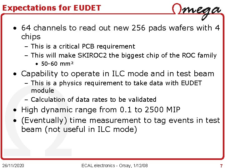
Expectations for EUDET • 64 channels to read out new 256 pads wafers with 4 chips – This is a critical PCB requirement – This will make SKIROC 2 the biggest chip of the ROC family • 50 -60 mm² • Capability to operate in ILC mode and in test beam – This is a physics requirement to take data with EUDET module – Calculation of data rates to be validated • High dynamic range from 0. 1 to 2500 MIP • (Eventually) time measurement to tag events in test beam (not useful in ILC mode) 26/11/2020 ECAL electronics - Orsay, 1/12/08 7
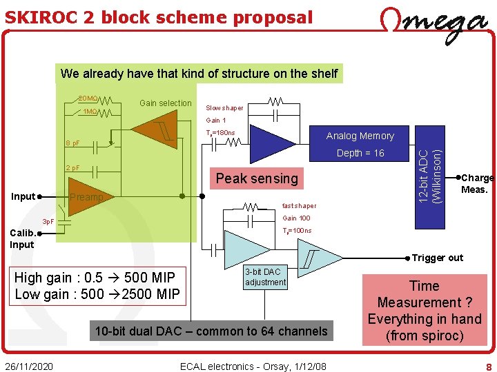
SKIROC 2 block scheme proposal We already have that kind of structure on the shelf 20 MΩ 1 MΩ Gain selection Slow shaper Gain 1 Tp=180 ns Depth = 16 2 p. F Input Peak sensing Preamp. fast shaper 12 -bit ADC (Wilkinson) Analog Memory 8 p. F Charge Meas. Gain 100 3 p. F Tp=100 ns Calib. Input Trigger out High gain : 0. 5 500 MIP Low gain : 500 2500 MIP 3 -bit DAC adjustment 10 -bit dual DAC – common to 64 channels 26/11/2020 ECAL electronics - Orsay, 1/12/08 Time Measurement ? Everything in hand (from spiroc) 8
Schedule • Skiroc 2 expected to be sent in fab in March’ 09 – Sharing of the HARDROC 2 and SPIROC 2 production – If SKIROC 2 is validated production in hand for EUDET module – Cheaper than an engineering run for prototyping due to big silicon area (60 mm² ie ~60 k€) • Next PCB prototype will use SPIROC 2 with Hamamatsu wafers – Validation of all electronics and assembling process – missing : dynamic range (500 MIP/2500 MIP), granularity – PCB in hand before the end of the year ? 26/11/2020 ECAL electronics - Orsay, 1/12/08 9
PCB design FEV 5 presentation 26/11/2020 ECAL electronics - Orsay, 1/12/08 10
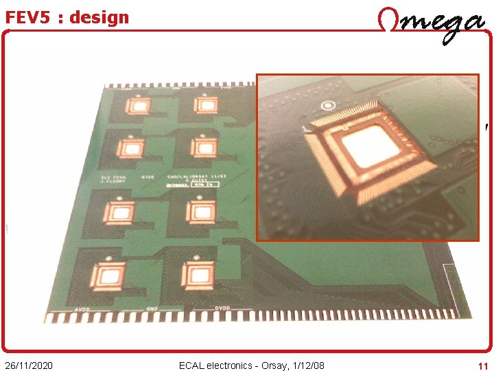
FEV 5 : design 18 c m HARDROC PCB WAFER 18 cm 1296 channels. 8 HARDROC (512 channels equipped) 26/11/2020 ECAL electronics - Orsay, 1/12/08 11
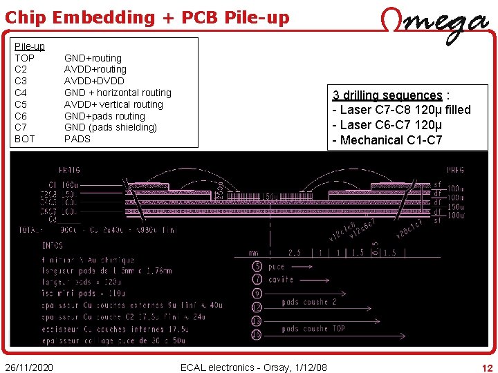
Chip Embedding + PCB Pile-up TOP C 2 C 3 C 4 C 5 C 6 C 7 BOT 26/11/2020 GND+routing AVDD+DVDD GND + horizontal routing AVDD+ vertical routing GND+pads routing GND (pads shielding) PADS 3 drilling sequences : - Laser C 7 -C 8 120µ filled - Laser C 6 -C 7 120µ - Mechanical C 1 -C 7 ECAL electronics - Orsay, 1/12/08 12
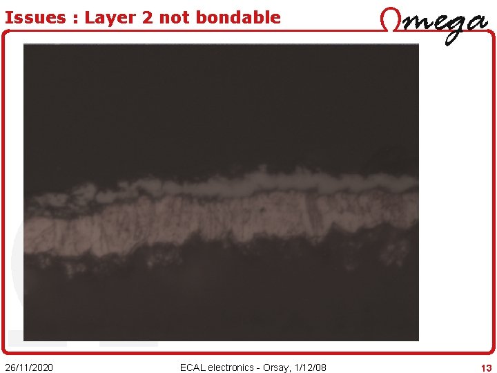
Issues : Layer 2 not bondable 26/11/2020 ECAL electronics - Orsay, 1/12/08 13
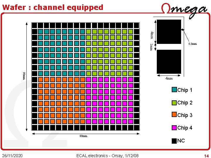
Wafer : channel equipped 4 mm 1 mm 0. 5 mm 90 mm 4 mm Chip 1 Chip 2 Chip 3 Chip 4 90 mm NC 26/11/2020 ECAL electronics - Orsay, 1/12/08 14
FEV 7 • First EUDET compliant PCB, using SPIROC 2 in SKIROC mode. • several pads merged for each electronics input • Halfway from expected granularity and physics prototype granularity 26/11/2020 ECAL electronics - Orsay, 1/12/08 15
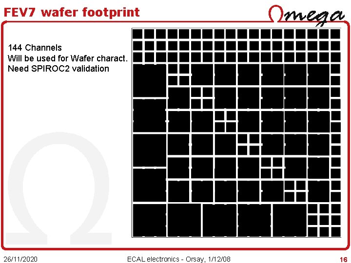
FEV 7 wafer footprint 144 Channels Will be used for Wafer charact. Need SPIROC 2 validation 26/11/2020 ECAL electronics - Orsay, 1/12/08 16
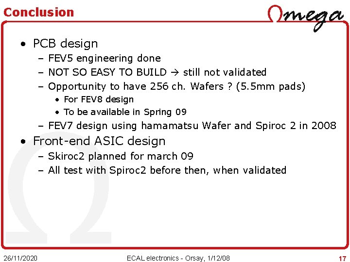
Conclusion • PCB design – FEV 5 engineering done – NOT SO EASY TO BUILD still not validated – Opportunity to have 256 ch. Wafers ? (5. 5 mm pads) • For FEV 8 design • To be available in Spring 09 – FEV 7 design using hamamatsu Wafer and Spiroc 2 in 2008 • Front-end ASIC design – Skiroc 2 planned for march 09 – All test with Spiroc 2 before then, when validated 26/11/2020 ECAL electronics - Orsay, 1/12/08 17