ASIC 120 Digital Systems and StandardCell ASIC Design




- Slides: 44

ASIC 120: Digital Systems and Standard-Cell ASIC Design Tutorial 4: Digital Systems Concepts November 16, 2005

Outline • Summary of previous tutorial • The FPGA: LEs, buffers and routing • Other FPGA resources: clocks, memories, memory interfaces, multipliers, etc. • Soft- and hard-processors in FPGAs • Bus interfaces • Register files

Summary of Previous Tutorial • • • Other signal values besides ‘ 0’ and ‘ 1’ More VHDL data types Attributes, type definitions Generics Splitting a VHDL project across multiple design units and files • if … generate, for … generate • VHDL 1987 vs. 1993 vs. 2000 • Test benches – time, procedures, variables, file access, etc.

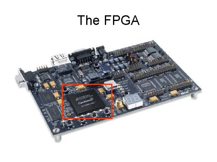
The FPGA • FPGA stands for Field Programmable Gate Array – reprogrammable hardware • FPGAs contain – Logic Elements (LEs) which do calculations – Routing resources between LEs – Other specialized functions (memory, multipliers, etc. )

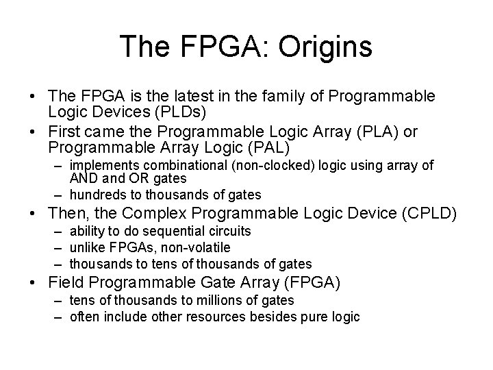
The FPGA: Origins • The FPGA is the latest in the family of Programmable Logic Devices (PLDs) • First came the Programmable Logic Array (PLA) or Programmable Array Logic (PAL) – implements combinational (non-clocked) logic using array of AND and OR gates – hundreds to thousands of gates • Then, the Complex Programmable Logic Device (CPLD) – ability to do sequential circuits – unlike FPGAs, non-volatile – thousands to tens of thousands of gates • Field Programmable Gate Array (FPGA) – tens of thousands to millions of gates – often include other resources besides pure logic

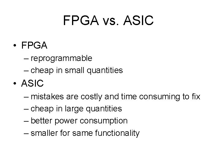
FPGA vs. ASIC • FPGA – reprogrammable – cheap in small quantities • ASIC – mistakes are costly and time consuming to fix – cheap in large quantities – better power consumption – smaller for same functionality

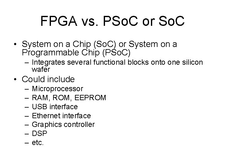
FPGA vs. PSo. C or So. C • System on a Chip (So. C) or System on a Programmable Chip (PSo. C) – Integrates several functional blocks onto one silicon wafer • Could include – – – – Microprocessor RAM, ROM, EEPROM USB interface Ethernet interface Graphics controller DSP etc.

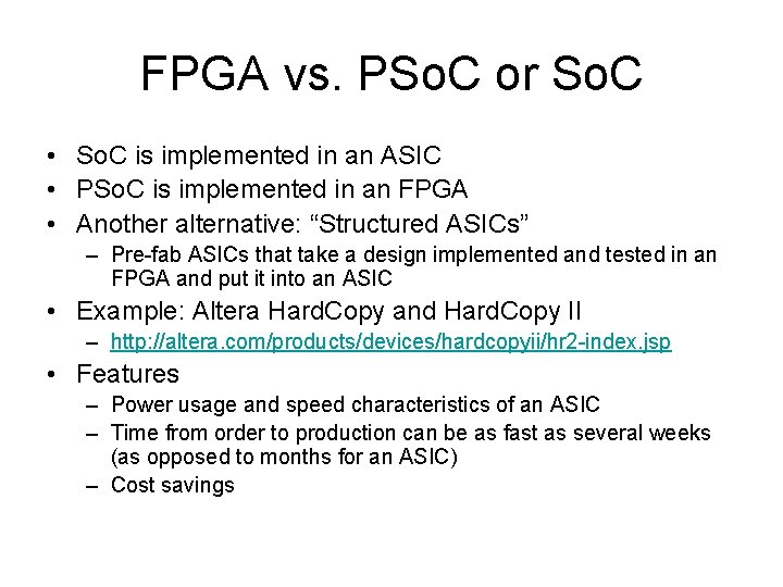
FPGA vs. PSo. C or So. C • So. C is implemented in an ASIC • PSo. C is implemented in an FPGA • Another alternative: “Structured ASICs” – Pre-fab ASICs that take a design implemented and tested in an FPGA and put it into an ASIC • Example: Altera Hard. Copy and Hard. Copy II – http: //altera. com/products/devices/hardcopyii/hr 2 -index. jsp • Features – Power usage and speed characteristics of an ASIC – Time from order to production can be as fast as several weeks (as opposed to months for an ASIC) – Cost savings

The FPGA

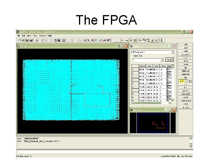
The FPGA

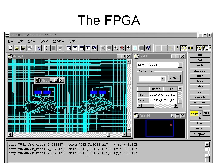
The FPGA

An FPGA Datasheet • Datasheets of any ASIC contain detailed specifications and technical data – FPGAs are no exception • Before you start any design, know the FPGA resources – – – size limitations speed limitations number of I/O pins clock pins and resources special features • You can never have enough FPGA resources

Components of an FPGA • • Logic Elements (LEs) Routing Input/Output logic Extra features – clocking – memory interfaces – multipliers

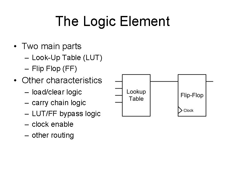
The Logic Element • Two main parts – Look-Up Table (LUT) – Flip Flop (FF) • Other characteristics – – – load/clear logic carry chain logic LUT/FF bypass logic clock enable other routing

The Logic Element • Look-Up Table – generally four inputs and one output – can implement any four input boolean expression • LEs maintain their configuration while power is applied to the FPGA – need to be re-programmed after power-up or global reset, and before using

Routing • Routing logic connects LEs to – other LEs – specialized FPGA resources – input/output pins • Different kinds of routing logic – short lines – long lines – carry chains – clock routing

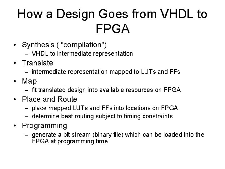
How a Design Goes from VHDL to FPGA • Synthesis ( “compilation”) – VHDL to intermediate representation • Translate – intermediate representation mapped to LUTs and FFs • Map – fit translated design into available resources on FPGA • Place and Route – place mapped LUTs and FFs into locations on FPGA – determine best routing subject to timing constraints • Programming – generate a bit stream (binary file) which can be loaded into the FPGA at programming time

How a Design Goes from VHDL to FPGA • This entire process is extremely nondeterministic – much more so than software compilation • Terms and steps on previous slide are “generic” – individual FPGA companies have their own terms and slightly different design flows

Input/Output Logic • I/O buffers – input – output – tri-state (“output enable”) • Specialized I/O – memory interfaces – high speed differential signalling • Modern FPGAs can be wired directly (with appropriate analog support components) to – – RAM chips 10/1000 Base-T Ethernet SD-SDI, HD-SDI drivers (up to 1. 5 Gbps) etc.

Extra FPGA Features • Clock features – Phase/Delay Locked Loops (PLLs/DLLs) – Special routing resources • Memory – Block RAM – Distributed RAM • Memory interfaces – SD-RAM, DDR 2, etc. – Configuration devices • Multipliers

Clocks • Modern FPGAs feature multiple onboard PLLs that can be used for – phase/frequency synchronization – frequency multiplication – arbitrary duty cycles • Clock routing logic – dedicated clock lines that run to all LEs – reduce clock jitter and skew • Generally external clocks must be connected to one of several special pins to use these features

Memory

Block RAM

Distributed RAM

RAM Inference

Memory Interfaces

FPGA Configuration • What happens to an FPGA on power-up? – LEs and RAM values are random, or some initialization value such as all 0 • An FPGA must be configured before it can be used – Configured by a microprocessor – Dedicated configuration device – CPLD using a non-volatile Flash RAM device

Multipliers

Hard- and Soft-Processors

Soft Processor Exmple: Altera NIOS-II

Hard Processor Example: Power. PC

Interfacing with FPGA Features in VHDL

Buses • A bus allows multiple entities to communicate over the same “wires” • External buses interface between physical ASICs or FPGAs • Internal buses interface between different components within an ASIC or FPGA

An Idle Bus

Bus Read Cycle

Bus Write Cycle

External Bus Interfaces

Internal Buses • Separate read and write buses

Buses: What I’ve Skipped • Bus arbitration – multiple masters • Direct Memory Access (DMA) – Bus mastering • See the E&CE 324 course notes for more on buses

Register Files • Also called register blocks

What I’ve Skipped • Blocks, Libraries/Packages – other modularity features – we’ve had a taste of libraries and packages: library ieee; … • Configurations – way to select among multiple architectures • Constants – like generics, but within one file • File access – useful for test benches, not synthesizable • Functions, procedures, variables

Preview of Next Tutorial • Digital Systems Concepts – The FPGA: LEs, buffers and routing, other resources – Bus interfaces – Register files – Other FPGA resources: clocks, memories, memory interfaces, multipliers, etc. – Soft- and hard-processors in FPGAs

Summary • • • Summary of previous tutorial Other signal values besides ‘ 0’ and ‘ 1’ More VHDL data types Attributes, type definitions Generics Splitting a VHDL project across multiple design units and files • if … generate, for … generate • VHDL 1987 vs. 1993 vs. 2000 • Test benches – time, procedures, variables, file access, etc.

UW ASIC Design Team • www. asic. uwaterloo. ca • reference material – Accolade VHDL reference (excellent!): http: //www. acc-eda. com/vhdlref/ • many of today’s examples came from here – Bryce Leung’s tutorials (UW ASIC website) – Mike Goldsmith’s tutorials (UW ASIC website) – your course notes • my contact info: Jeff Wentworth, jswentwo@engmail. uwaterloo. ca