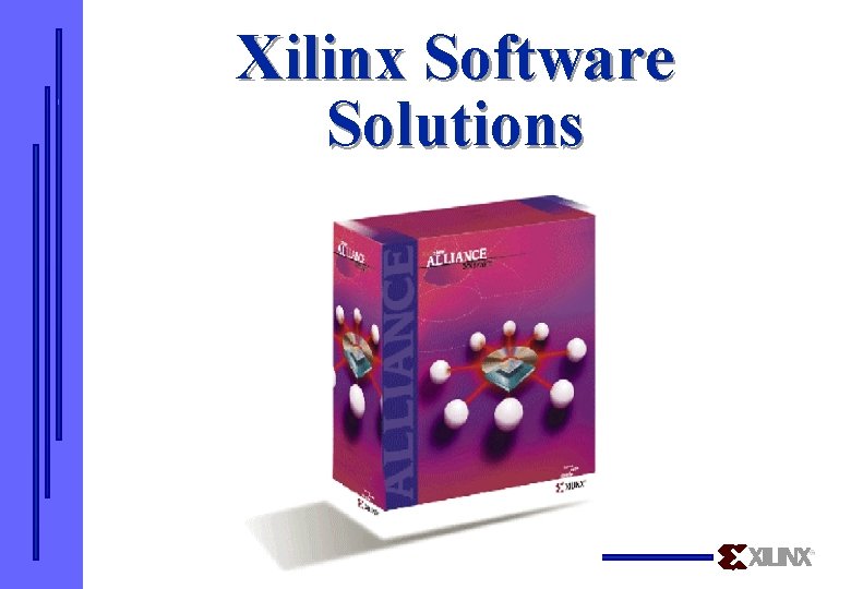
Xilinx Software Solutions Xilinx Software Series Alliance Series




- Slides: 89

Xilinx Software Solutions

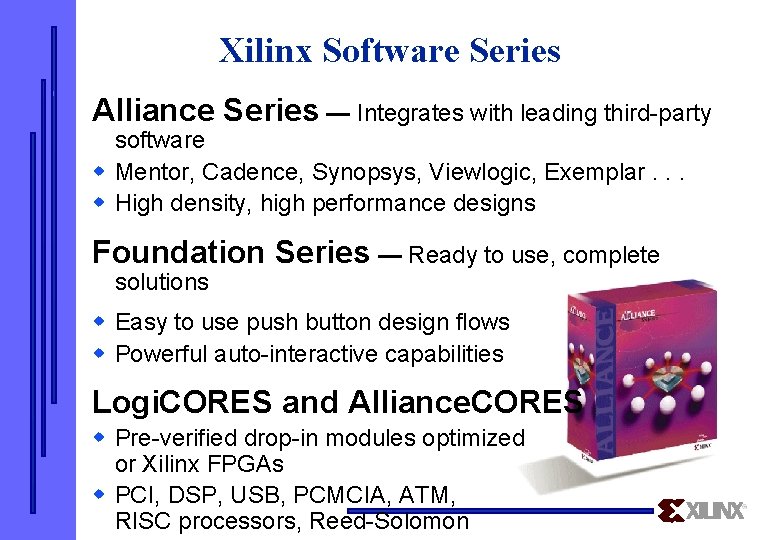
Xilinx Software Series Alliance Series — Integrates with leading third-party software w Mentor, Cadence, Synopsys, Viewlogic, Exemplar. . . w High density, high performance designs Foundation Series — Ready to use, complete solutions w Easy to use push button design flows w Powerful auto-interactive capabilities Logi. CORES and Alliance. CORES w Pre-verified drop-in modules optimized or Xilinx FPGAs w PCI, DSP, USB, PCMCIA, ATM, RISC processors, Reed-Solomon

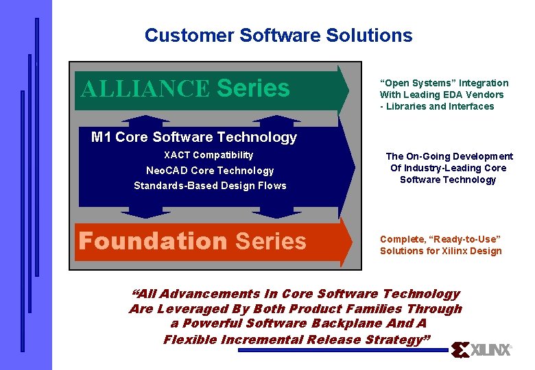
Customer Software Solutions ALLIANCE Series “Open Systems” Integration With Leading EDA Vendors - Libraries and Interfaces M 1 Core Software Technology Foundation XACT Compatibility M 1 Core Technology Neo. CAD Core. Backplane Technology Standards-Based Design Flows Foundation Series The On-Going Development Of Industry-Leading Core Software Technology Complete, “Ready-to-Use” Solutions for Xilinx Design “All Advancements In Core Software Technology Are Leveraged By Both Product Families Through a Powerful Software Backplane And A Flexible Incremental Release Strategy”

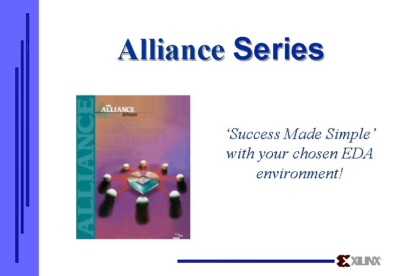
Alliance Series ‘Success Made Simple’ with your chosen EDA environment!

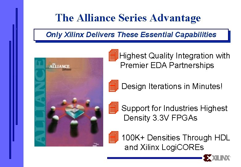
The Alliance Series Advantage Only Xilinx Delivers These Essential Capabilities Highest Quality Integration with Premier EDA Partnerships Design Iterations in Minutes! Support for Industries Highest Density 3. 3 V FPGAs 100 K+ Densities Through HDL and Xilinx Logi. COREs

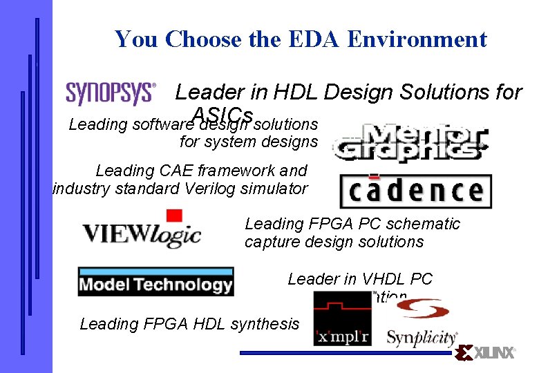
You Choose the EDA Environment Leader in HDL Design Solutions for Leading software. ASICs design solutions for system designs Leading CAE framework and industry standard Verilog simulator Leading FPGA PC schematic capture design solutions Leader in VHDL PC simulation Leading FPGA HDL synthesis

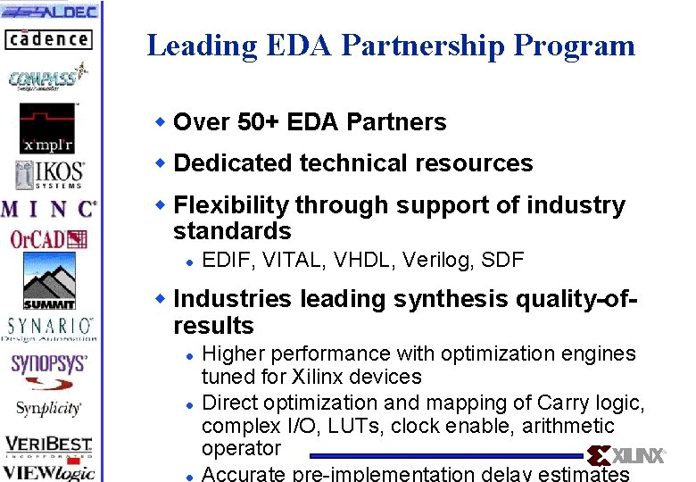
Leading EDA Partnership Program w Over 50+ EDA Partners w Dedicated technical resources w Flexibility through support of industry standards l EDIF, VITAL, VHDL, Verilog, SDF w Industries leading synthesis quality-ofresults l l l Higher performance with optimization engines tuned for Xilinx devices Direct optimization and mapping of Carry logic, complex I/O, LUTs, clock enable, arithmetic operator Accurate pre-implementation delay estimates

Xilinx Software Technology: Gives You a Performance Advantage w Performance Improvements — Maximizes Clock Rate w Advanced Methodology Support — Increases designer productivity w Utilization Improvements — > 95% Utilization w Up to 70% shorter runtimes w Robust Timing Language with SMART specs. TM

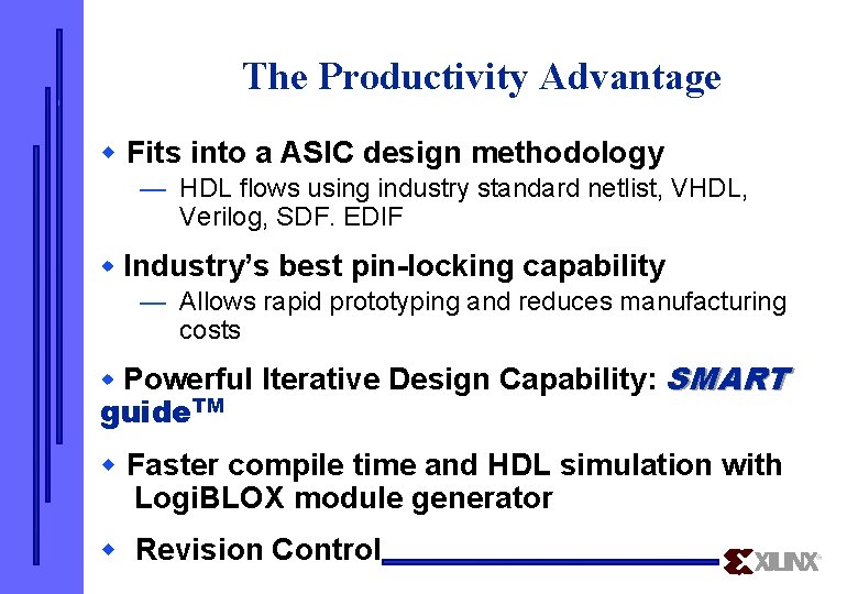
The Productivity Advantage w Fits into a ASIC design methodology — HDL flows using industry standard netlist, VHDL, Verilog, SDF. EDIF w Industry’s best pin-locking capability — Allows rapid prototyping and reduces manufacturing costs w Powerful Iterative Design Capability: guide. TM SMART w Faster compile time and HDL simulation with Logi. BLOX module generator w Revision Control

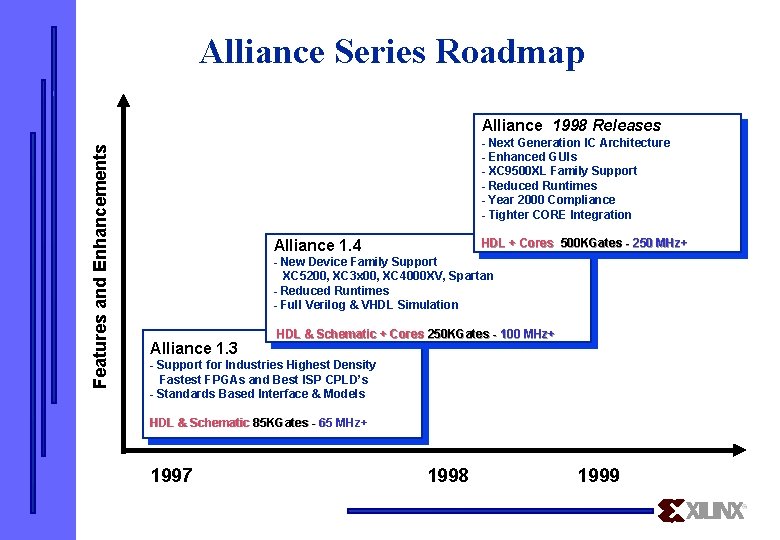
Alliance Series Roadmap Features and Enhancements Alliance 1998 Releases - Next Generation IC Architecture - Enhanced GUIs - XC 9500 XL Family Support - Reduced Runtimes - Year 2000 Compliance - Tighter CORE Integration Alliance 1. 4 HDL + Cores 500 KGates - 250 MHz+ - New Device Family Support XC 5200, XC 3 x 00, XC 4000 XV, Spartan - Reduced Runtimes - Full Verilog & VHDL Simulation Alliance 1. 3 HDL & Schematic + Cores 250 KGates - 100 MHz+ - Support for Industries Highest Density Fastest FPGAs and Best ISP CPLD’s - Standards Based Interface & Models HDL & Schematic 85 KGates - 65 MHz+ 1997 1998 1999

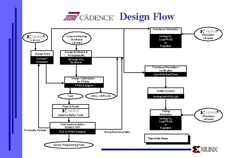
Design Flow Functional Simulation X-BLOX Cadence/Synergy Synthesis Libraries Design Entry Design Synthesis & Retargetability Concept / Composer Synergy HDL Synthesis Verilog XL, Leap. FROG or Rapidsim Simulation Libraries Functional Simulation / Verification Open. SIM Back. Plane Design Optimization for FPGAs FPGA Designer Netlist Creation *XNF VHDL, VERILOG Verilog. Link/VHDLLink Place & Route Timing Simulation Implementation Tools Schematic Redraw Verilog-XL, Leap. FROG or Rapidsim Post Implementation Netlist & SDF PLD & FPGA Designer Timing Backannotation *Xilinx Device Programming Files Netlist Format Simulation Libraries

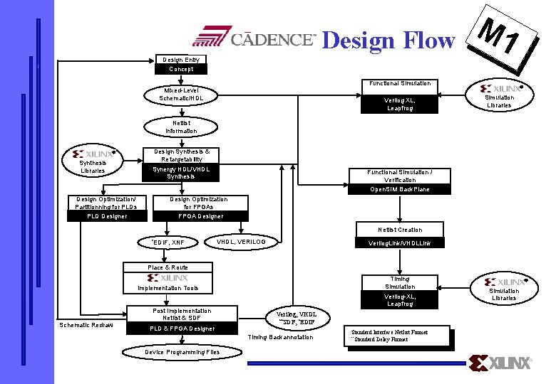
M 1 Design Flow Design Entry Concept Functional Simulation Mixed-Level Schematic/HDL Verilog XL, Leapfrog Simulation Libraries Netlist Information Synthesis Libraries Design Synthesis & Retargetability Synergy HDL/VHDL Synthesis Functional Simulation / Verification Open. SIM Back. Plane Design Optimization for FPGAs Design Optimization/ Partitionning for PLDs PLD Designer FPGA Designer Netlist Creation *EDIF, XNF VHDL, VERILOG Verilog. Link/VHDLLink Place & Route Timing Simulation Implementation Tools Schematic Redraw Post Implementation Netlist & SDF PLD & FPGA Designer Verilog-XL, Leapfrog Verilog, VHDL **SDF, *EDIF Timing Backannotation Device Programming Files *Standard Interface Netlist Format Delay Format ** Standard Simulation Libraries

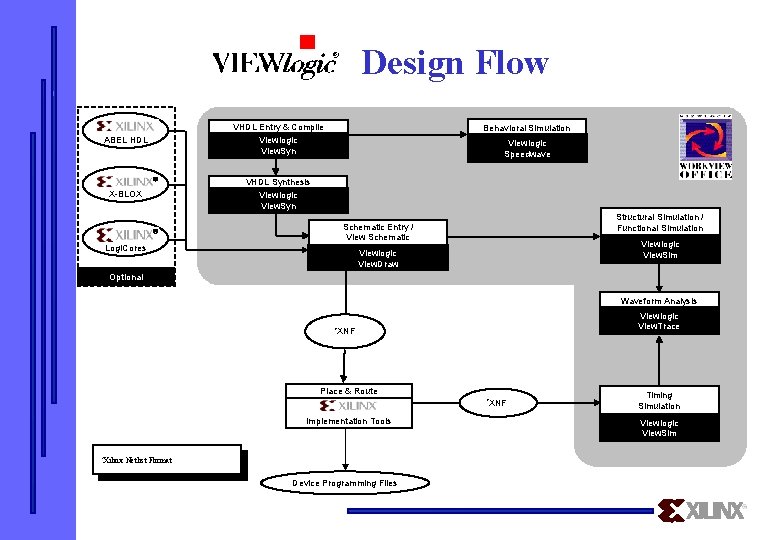
Design Flow ABEL HDL VHDL Entry & Compile Viewlogic View. Syn X-BLOX VHDL Synthesis Viewlogic View. Syn Behavioral Simulation Viewlogic Speedwave Structural Simulation / Functional Simulation Schematic Entry / View Schematic Logi. Cores Viewlogic View. Sim Viewlogic View. Draw Optional Waveform Analysis Viewlogic View. Trace *XNF Place & Route *XNF Implementation Tools *Xilinx Netlist Format Device Programming Files Timing Simulation Viewlogic View. Sim

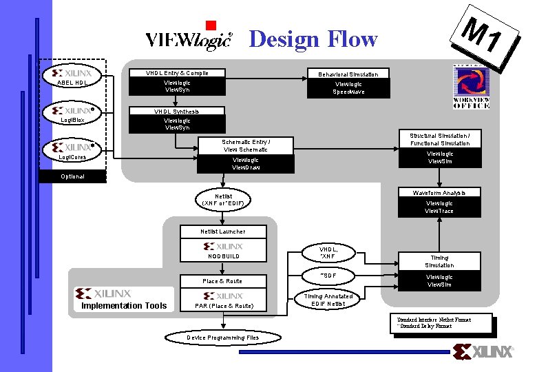
M 1 Design Flow ABEL HDL VHDL Entry & Compile Viewlogic View. Syn Logi. Blox VHDL Synthesis Viewlogic View. Syn Behavioral Simulation Viewlogic Speedwave Structural Simulation / Functional Simulation Schematic Entry / View Schematic Logi. Cores Viewlogic View. Sim Viewlogic View. Draw Optional Waveform Analysis Netlist (XNF or *EDIF) Viewlogic View. Trace Netlist Launcher NGDBUILD Place & Route Implementation Tools PAR (Place & Route) VHDL, *XNF Timing Simulation **SDF Viewlogic View. Sim Timing Annotated EDIF Netlist *Standard Interface Netlist Format Delay Format ** Standard Device Programming Files

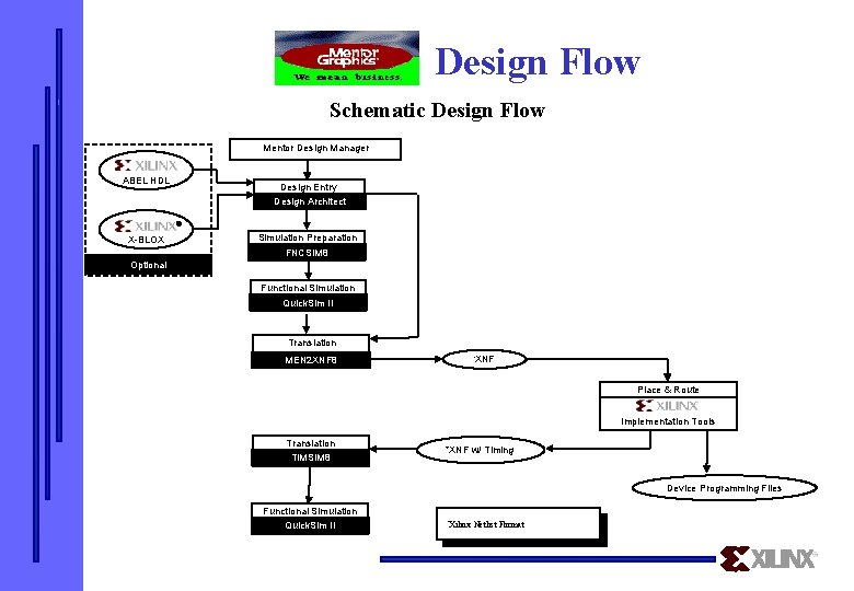
Design Flow Schematic Design Flow Mentor Design Manager ABEL HDL Design Entry Design Architect X-BLOX Simulation Preparation FNCSIM 8 Optional Functional Simulation Quick. Sim II Translation XNF * MEN 2 XNF 8 Place & Route Implementation Tools Translation TIMSIM 8 *XNF w/ Timing Device Programming Files Functional Simulation Quick. Sim II *Xilinx Netlist Format

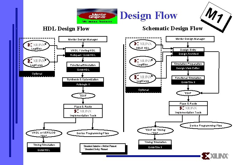
M 1 Design Flow HDL Design Flow Schematic Design Flow Mentor Design Manager Logi. Blox VHDL / Verilog HDL ABLE HDL Notepad / Quick. HDL Logi. Cores Functional. Simulation Design Entry Design Architect Logi. Blox Quick. HDL Simulation Preparation Design View Editor Optional Synthesis & Optomization Functional Simulation Logi. Cores Autologic II Quick. Sim II Optional *EDIF Place & Route Implementation Tools Device Programming Files VHDL or VERILOG *SDF Timing Simulation Quick. HDL Device Programming Files *EDIF w/ Timing *SDF Timing Simulation *Standard Interface Netlist Format ** Standard Delay Format Quick. Sim II

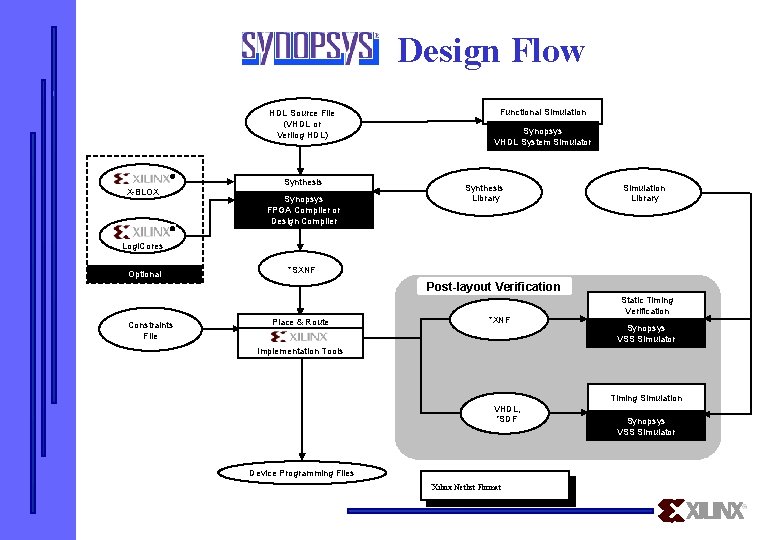
Design Flow Functional Simulation HDL Source File (VHDL or Verilog HDL) X-BLOX Synopsys VHDL System Simulator Synthesis Library Synopsys FPGA Compiler or Design Compiler Simulation Library Logi. Cores Optional *SXNF Post-layout Verification Constraints File *XNF Place & Route Static Timing Verification Synopsys VSS Simulator Implementation Tools Timing Simulation VHDL, *SDF Device Programming Files *Xilinx Netlist Format Synopsys VSS Simulator

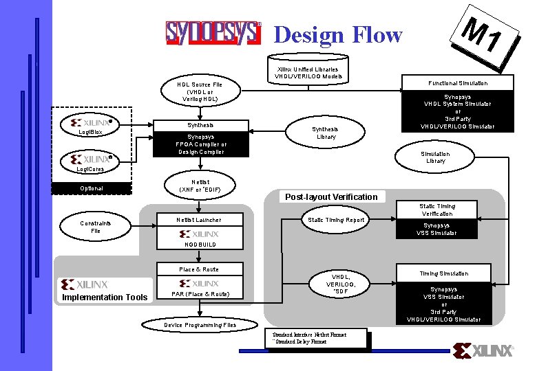
M 1 Design Flow Xilinx Unified Libraries VHDL/VERILOG Models HDL Source File (VHDL or Verilog HDL) Logi. Blox Synthesis Library Synopsys FPGA Compiler or Design Compiler Functional Simulation Synopsys VHDL System Simulator or 3 rd Party VHDL/VERILOG Simulator Simulation Library Logi. Cores Optional Constraints File Netlist (XNF or *EDIF) Post-layout Verification Netlist Launcher Static Timing Report Static Timing Verification Synopsys VSS Simulator NGDBUILD Place & Route Implementation Tools VHDL, VERILOG, *SDF PAR (Place & Route) Device Programming Files *Standard Interface Netlist Format Delay Format ** Standard Timing Simulation Synopsys VSS Simulator or 3 rd Party VHDL/VERILOG Simulator

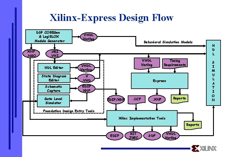
Xilinx-Express Design Flow DSP COREGen & Logi. BLOX Module Generator XNF. NGO VHDL Verilog Behavioral Simulation Models . VEI. VHI HDL Editor VHDL Verilog State Diagram Editor . V. VHD Schematic Capture EDIF XNF Gate Level Simulator VHDL Verilog Timing Requirements S I M U L A T I O N Express EDIF/XNF . UCF Reports . XNF Foundation Design Entry Tools Xilinx Implementation Tools Reports EDIF BIT JDEC SDF VHDL Verilog H D L

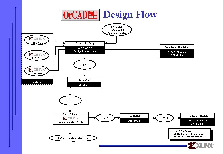
Design Flow XNF modules (Created by HDL Synthesis tools) ABEL HDL Schematic Entry Functional Simulation Or. CAD/ESP Design Environment Or. CAD Simulate XSim. Make X-BLOX **SDT Logi. Cores Translation Optional SDT 2 XNF *XNF Place & Route *XNF Implementation Tools Translation XNF 2 VST Timing Simulation *** VST Or. CAD Simulate XSim. Make *Xilinx Netlist Format Schematic Design Format ** Or. CAD Simulation File Format ** Or. CAD Device Programming Files

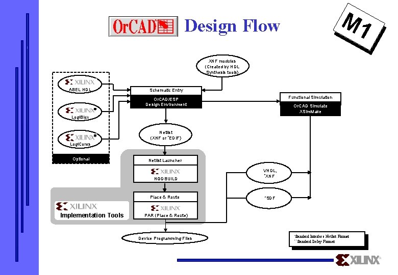
M 1 Design Flow XNF modules (Created by HDL Synthesis tools) ABEL HDL Schematic Entry Functional Simulation Or. CAD/ESP Design Environment Or. CAD Simulate XSim. Make Logi. Blox Netlist (XNF or *EDIF) Logi. Cores Optional Netlist Launcher NGDBUILD Place & Route Implementation Tools VHDL, *XNF *SDF PAR (Place & Route) Device Programming Files *Standard Interface Netlist Format Delay Format ** Standard

Xilinx Foundation Series Easy Of Use & VHDL Design in Minutes

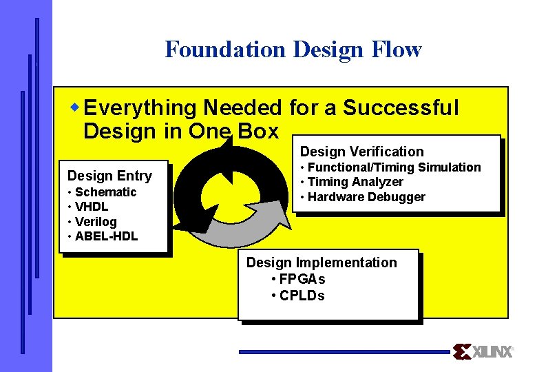
Foundation Design Flow w Everything Needed for a Successful Design in One Box Design Verification Design Entry • Schematic • VHDL • Verilog • ABEL-HDL • Functional/Timing Simulation • Timing Analyzer • Hardware Debugger Design Implementation • FPGAs • CPLDs

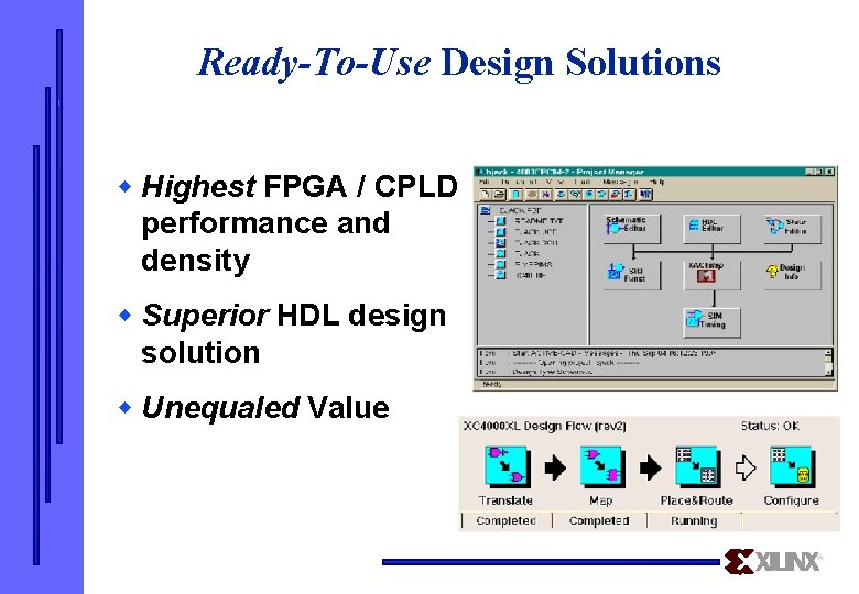
Ready-To-Use Design Solutions w Highest FPGA / CPLD performance and density w Superior HDL design solution w Unequaled Value

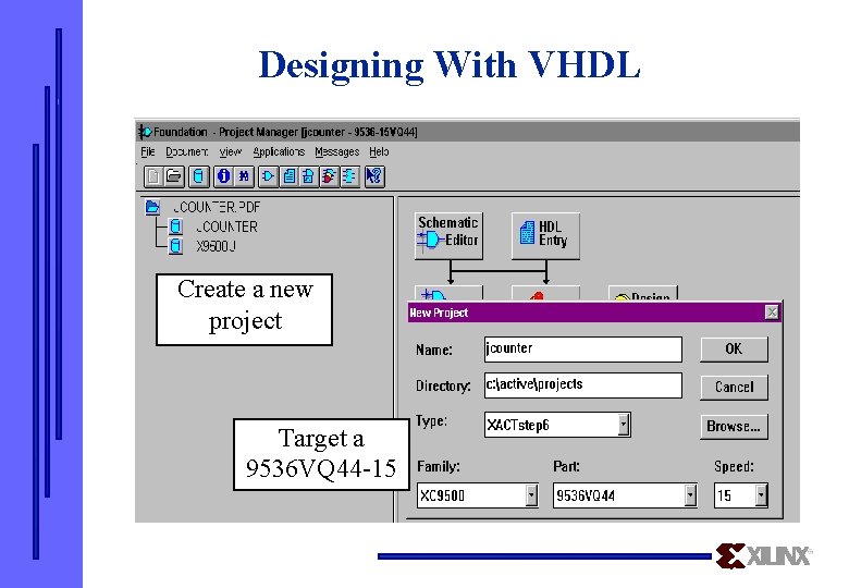
Designing With VHDL Create a new project Target a 9536 VQ 44 -15

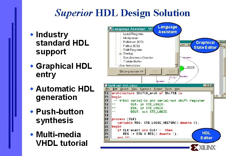
Superior HDL Design Solution w Industry standard HDL support Language Assistant Graphical State Editor w Graphical HDL entry w Automatic HDL generation w Push-button synthesis w Multi-media VHDL tutorial HDL Editor

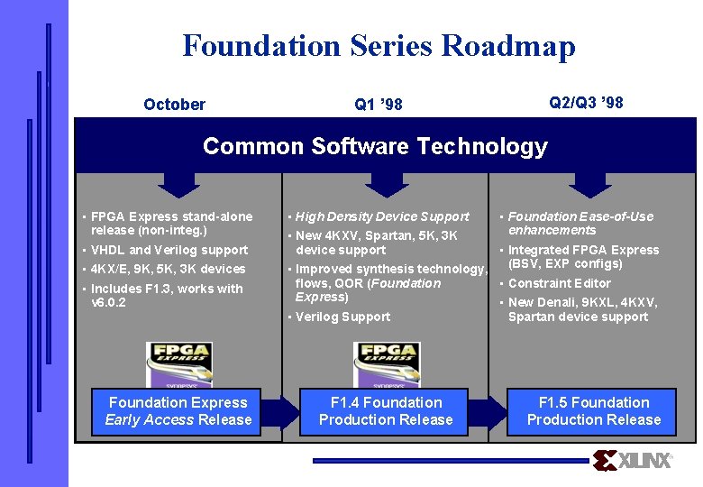
Foundation Series Roadmap October Q 2/Q 3 ’ 98 Q 1 ’ 98 Common Software Technology • FPGA Express stand-alone release (non-integ. ) • High Density Device Support • VHDL and Verilog support • Integrated FPGA Express (BSV, EXP configs) • Improved synthesis technology, flows, QOR (Foundation • Constraint Editor Express) • New Denali, 9 KXL, 4 KXV, • 4 KX/E, 9 K, 5 K, 3 K devices • Includes F 1. 3, works with v 6. 0. 2 Foundation Express Early Access Release • New 4 KXV, Spartan, 5 K, 3 K device support • Verilog Support F 1. 4 Foundation Production Release • Foundation Ease-of-Use enhancements Spartan device support F 1. 5 Foundation Production Release

XACTstep M 1

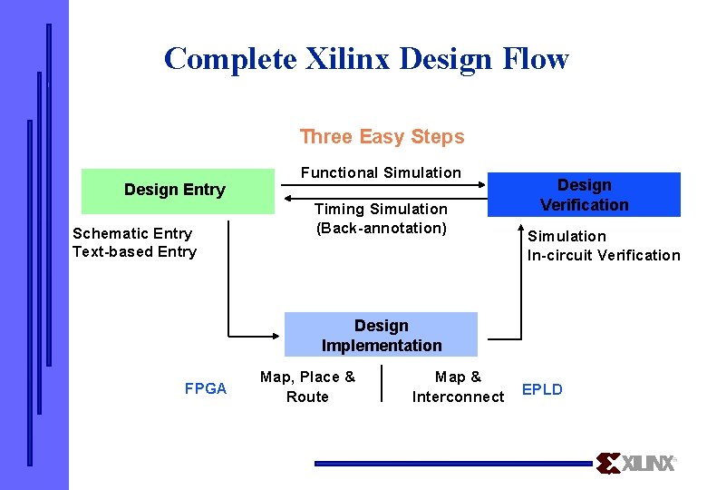
Complete Xilinx Design Flow Three Easy Steps Design Entry Schematic Entry Text-based Entry Functional Simulation Timing Simulation (Back-annotation) Design Verification Simulation In-circuit Verification Design Implementation FPGA Map, Place & Route Map & Interconnect EPLD

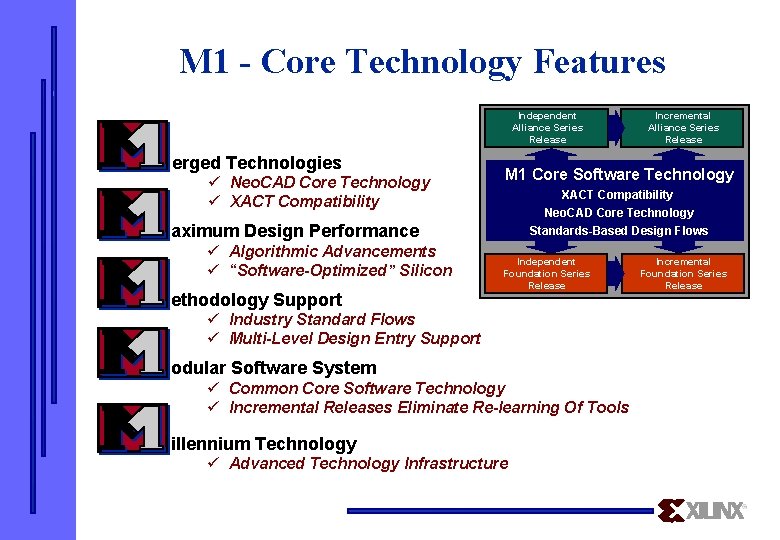
M 1 - Core Technology Features Independent Alliance Series Release erged Technologies ü Neo. CAD Core Technology ü XACT Compatibility M 1 Core Software Technology XACT Compatibility Neo. CAD Core Technology Standards-Based Design Flows M 1 Core Technology Backplane aximum Design Performance ü Algorithmic Advancements ü “Software-Optimized” Silicon ethodology Support Incremental Alliance Series Release Independent Foundation Series Release ü Industry Standard Flows ü Multi-Level Design Entry Support odular Software System ü Common Core Software Technology ü Incremental Releases Eliminate Re-learning Of Tools illennium Technology ü Advanced Technology Infrastructure Incremental Foundation Series Release

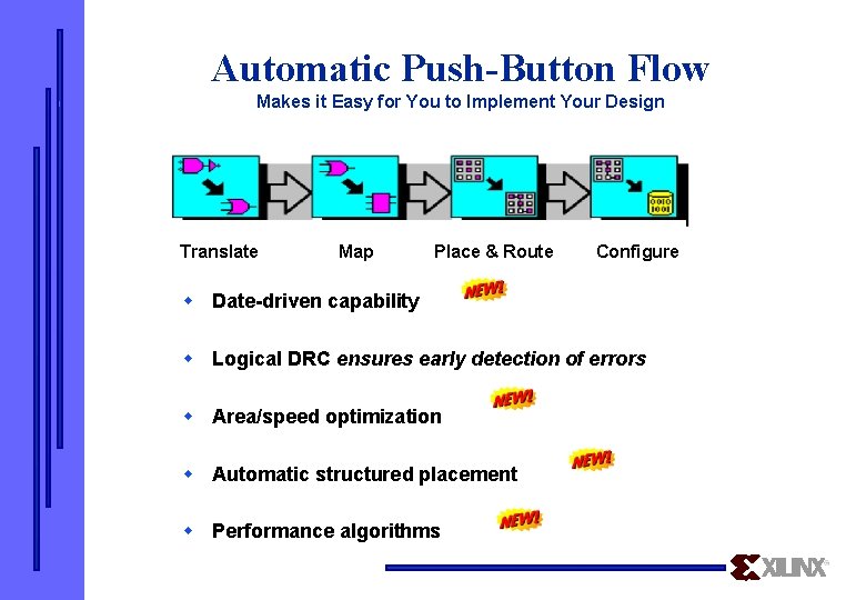
Automatic Push-Button Flow Makes it Easy for You to Implement Your Design Translate Map Place & Route Configure w Date-driven capability w Logical DRC ensures early detection of errors w Area/speed optimization w Automatic structured placement w Performance algorithms

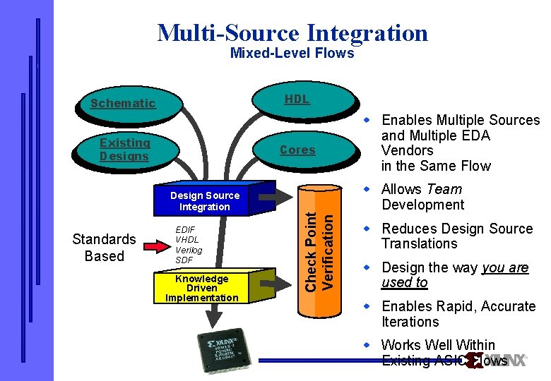
Multi-Source Integration Mixed-Level Flows HDL Schematic Existing Designs Design Source Integration Standards Based EDIF VHDL Verilog SDF Knowledge Driven Implementation Check Point Verification Cores w Enables Multiple Sources and Multiple EDA Vendors in the Same Flow w Allows Team Development w Reduces Design Source Translations w Design the way you are used to w Enables Rapid, Accurate Iterations w Works Well Within Existing ASIC Flows w Facilitates Design Reuse

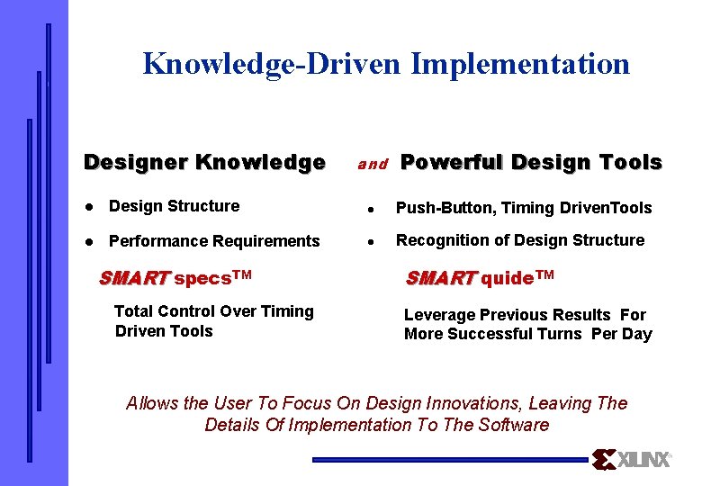
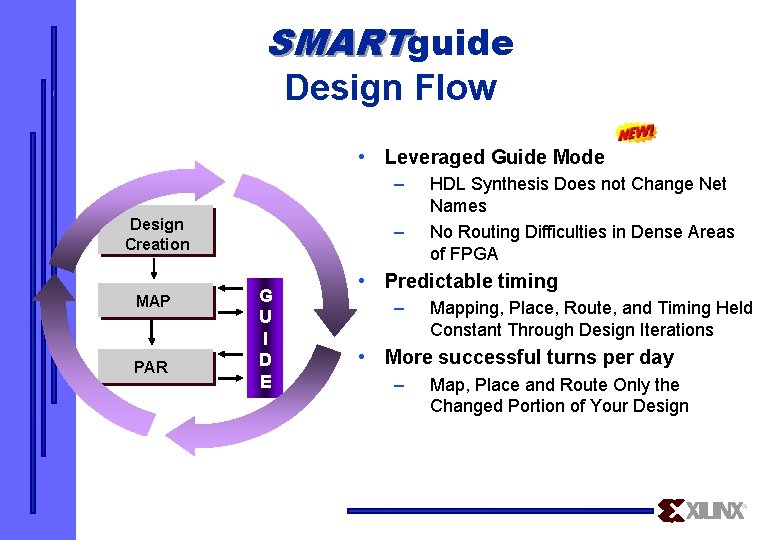
Knowledge-Driven Implementation Designer Knowledge and Powerful Design Tools l Design Structure l Push-Button, Timing Driven. Tools l Performance Requirements l Recognition of Design Structure SMART specs. TM Total Control Over Timing Driven Tools SMART quide. TM Leverage Previous Results For More Successful Turns Per Day Allows the User To Focus On Design Innovations, Leaving The Details Of Implementation To The Software

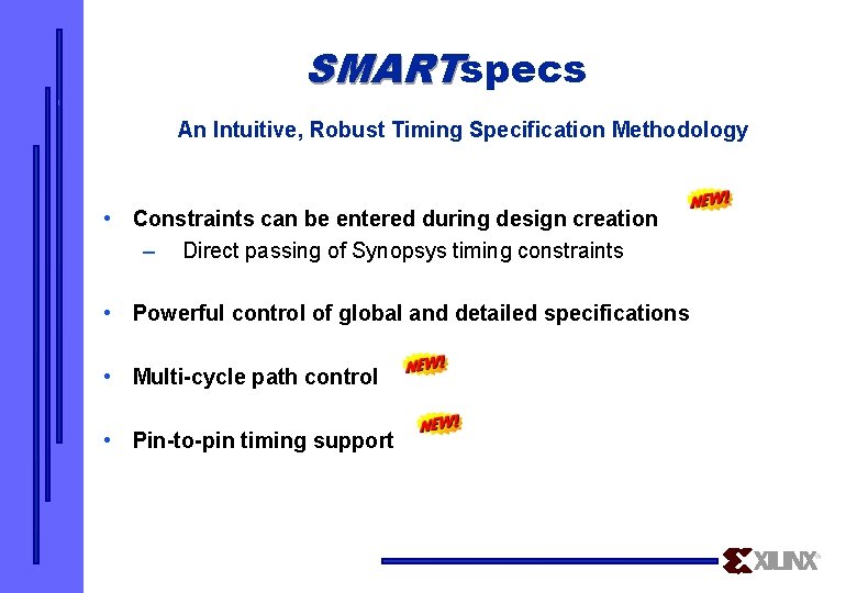
SMARTspecs An Intuitive, Robust Timing Specification Methodology • Constraints can be entered during design creation – Direct passing of Synopsys timing constraints • Powerful control of global and detailed specifications • Multi-cycle path control • Pin-to-pin timing support

SMARTguide Design Flow • Leveraged Guide Mode – Design Creation MAP PAR – G U I D E HDL Synthesis Does not Change Net Names No Routing Difficulties in Dense Areas of FPGA • Predictable timing – Mapping, Place, Route, and Timing Held Constant Through Design Iterations • More successful turns per day – Map, Place and Route Only the Changed Portion of Your Design

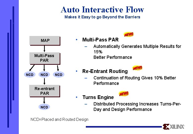
Auto Interactive Flow Makes it Easy to go Beyond the Barriers • Multi-Pass PAR MAP – Multi-Pass PAR NCD Re-entrant PAR NCD Automatically Generates Multiple Results for 15% Better Performance • Re-Entrant Routing – Continuation of Routing Gives 10% Better Performance • Turns Engine – NCD=Placed and Routed Design Distributed Processing Increases Turns-Per. Day and Design Performance

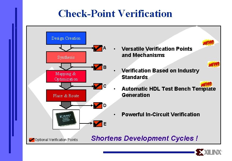
Check-Point Verification Design Creation A • Versatile Verification Points and Mechanisms • Verification Based on Industry Standards • Automatic HDL Test Bench Template Generation • Powerful In-Circuit Verification Synthesis B Mapping & Optimization C Place & Route D E = Optional Verification Points Shortens Development Cycles !

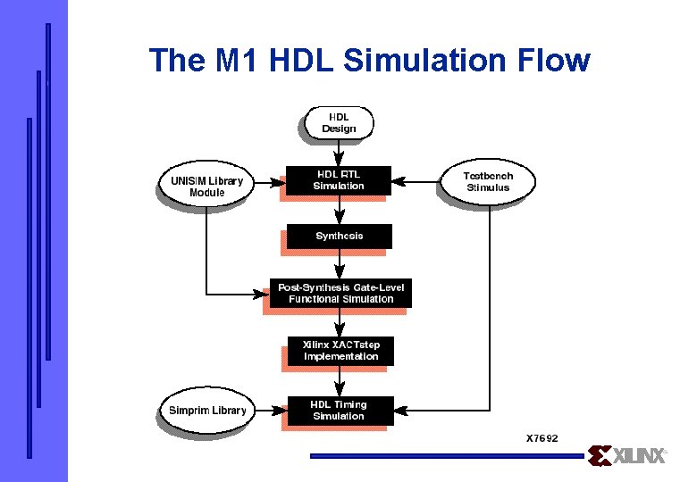
The M 1 HDL Simulation Flow

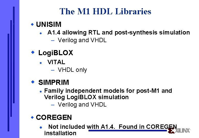
The M 1 HDL Libraries w UNISIM l A 1. 4 allowing RTL and post-synthesis simulation – Verilog and VHDL w Logi. BLOX l VITAL – VHDL only w SIMPRIM l Family independent models for post-M 1 and Verilog Logi. BLOX simulation – Verilog and VHDL w COREGEN l Not included with A 1. 4. Found in COREGEN installation

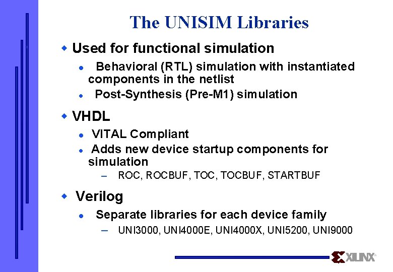
The UNISIM Libraries w Used for functional simulation l l Behavioral (RTL) simulation with instantiated components in the netlist Post-Synthesis (Pre-M 1) simulation w VHDL l l VITAL Compliant Adds new device startup components for simulation – ROC, ROCBUF, TOCBUF, STARTBUF w Verilog l Separate libraries for each device family – UNI 3000, UNI 4000 E, UNI 4000 X, UNI 5200, UNI 9000

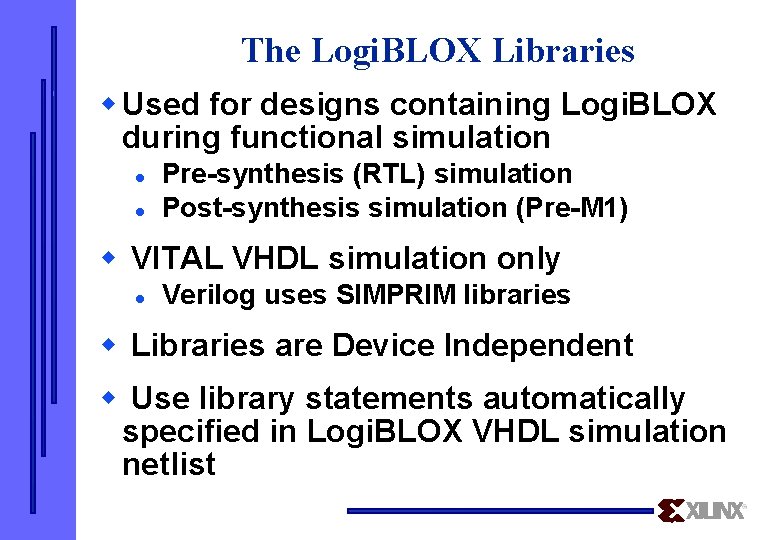
The Logi. BLOX Libraries w Used for designs containing Logi. BLOX during functional simulation l l Pre-synthesis (RTL) simulation Post-synthesis simulation (Pre-M 1) w VITAL VHDL simulation only l Verilog uses SIMPRIM libraries w Libraries are Device Independent w Use library statements automatically specified in Logi. BLOX VHDL simulation netlist

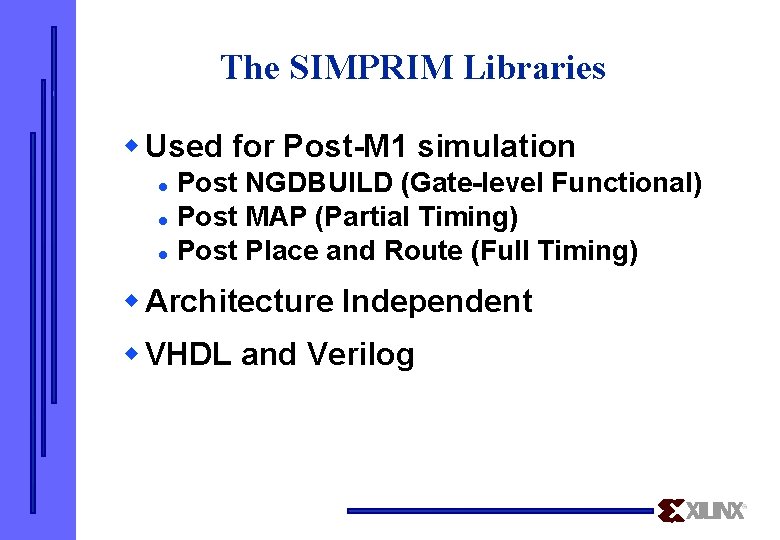
The SIMPRIM Libraries w Used for Post-M 1 simulation Post NGDBUILD (Gate-level Functional) l Post MAP (Partial Timing) l Post Place and Route (Full Timing) l w Architecture Independent w VHDL and Verilog

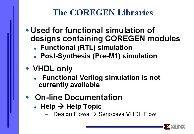
The COREGEN Libraries w Used for functional simulation of designs containing COREGEN modules l l Functional (RTL) simulation Post-Synthesis (Pre-M 1) simulation w VHDL only l Functional Verilog simulation is not currently available w On-line Documentation l Help Topic – Design Flows Synopsys VHDL Flow

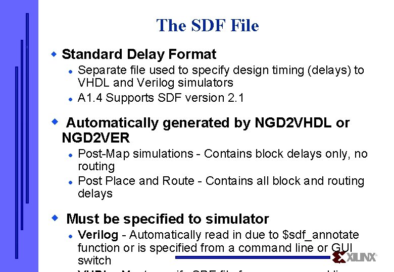
The SDF File w Standard Delay Format l l Separate file used to specify design timing (delays) to VHDL and Verilog simulators A 1. 4 Supports SDF version 2. 1 w Automatically generated by NGD 2 VHDL or NGD 2 VER l l Post-Map simulations - Contains block delays only, no routing Post Place and Route - Contains all block and routing delays w Must be specified to simulator l Verilog - Automatically read in due to $sdf_annotate function or is specified from a command line or GUI switch

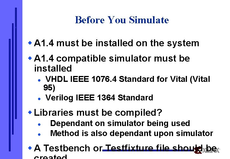
Before You Simulate w A 1. 4 must be installed on the system w A 1. 4 compatible simulator must be installed VHDL IEEE 1076. 4 Standard for Vital (Vital 95) l Verilog IEEE 1364 Standard l w Libraries must be compiled? l l Dependant on simulator being used Method is also dependant upon simulator w A Testbench or Testfixture file should be

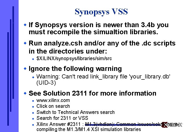
Synopsys VSS w If Synopsys version is newer than 3. 4 b you must recompile the simualtion libraries. w Run analyze. csh and/or any of the. dc scripts in the directories under: l $XILINX/synopsys/libraries/sim/src w Ignore the following warning l Warning: Can't read link_library file 'your_library. db' (UID-3) w See Solution 2311 for more information l l l www. xilinx. com Click on search Switch to Technical Answers search Search for 2311 or VSS Xilinx Answer #2311 : M 1. 3(vhdlan): Common issues/solutions recompiling the M 1. 3/M 1. 4 XSI simulation libraries

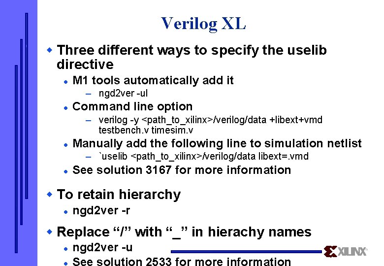
Verilog XL w Three different ways to specify the uselib directive l M 1 tools automatically add it – ngd 2 ver -ul l Command line option – verilog -y <path_to_xilinx>/verilog/data +libext+vmd testbench. v timesim. v l Manually add the following line to simulation netlist – `uselib <path_to_xilinx>/verilog/data libext=. vmd l See solution 3167 for more information w To retain hierarchy l ngd 2 ver -r w Replace “/” with “_” in hierachy names l l ngd 2 ver -u See solution 2533 for more information

Library Compilation

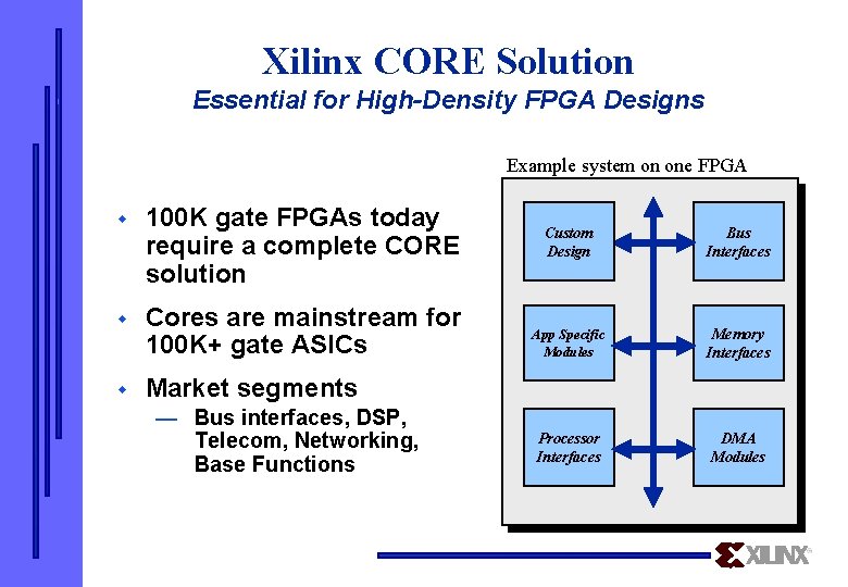
Xilinx CORE Solution Essential for High-Density FPGA Designs Example system on one FPGA w 100 K gate FPGAs today require a complete CORE solution w Cores are mainstream for 100 K+ gate ASICs w Market segments — Bus interfaces, DSP, Telecom, Networking, Base Functions Custom Design Bus Interfaces App Specific Modules Memory Interfaces Processor Interfaces DMA Modules

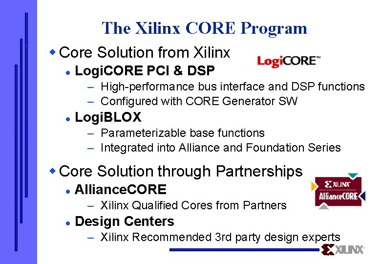
The Xilinx CORE Program w Core Solution from Xilinx l Logi. CORE PCI & DSP – High-performance bus interface and DSP functions – Configured with CORE Generator SW l Logi. BLOX – Parameterizable base functions – Integrated into Alliance and Foundation Series w Core Solution through Partnerships l Alliance. CORE – Xilinx Qualified Cores from Partners l Design Centers – Xilinx Recommended 3 rd party design experts

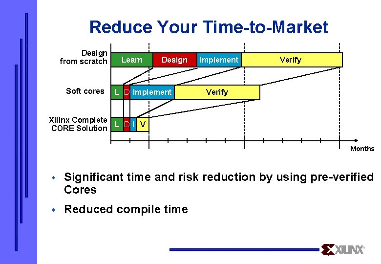
Reduce Your Time-to-Market Design from scratch Soft cores Learn Design L D Implement Verify Xilinx Complete CORE Solution L D I V Months w Significant time and risk reduction by using pre-verified Cores w Reduced compile time

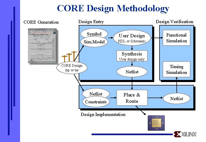
CORE Design Methodology CORE Generation Design Entry Design Verification Symbol User Design Sim. Model HDL or Schematic Functional Simulation Synthesis User design only CORE Design zip or tar Netlist Constraints Netlist Timing Simulation Place & Route Netlist Design Implementation

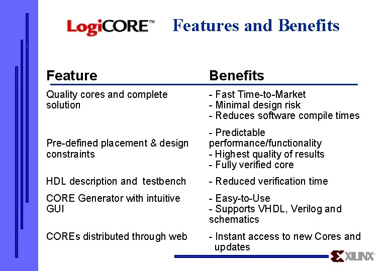
CORE Features and Benefits Feature Benefits Quality cores and complete solution - Fast Time-to-Market - Minimal design risk - Reduces software compile times Pre-defined placement & design constraints - Predictable performance/functionality - Highest quality of results - Fully verified core HDL description and testbench - Reduced verification time CORE Generator with intuitive GUI - Easy-to-Use - Supports VHDL, Verilog and schematics COREs distributed through web - Instant access to new Cores and updates

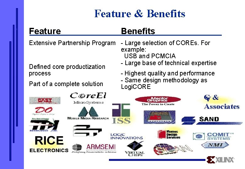
E Feature & Benefits Feature Benefits Extensive Partnership Program - Large selection of COREs. For example: USB and PCMCIA - Large base of technical expertise Defined core productization process - Highest quality and performance - Same design methodology as Part of a complete solution Logi. CORE - Docs, hardware and software

DSP Applications with the Xilinx CORE Generator and DSP Logi. COREs

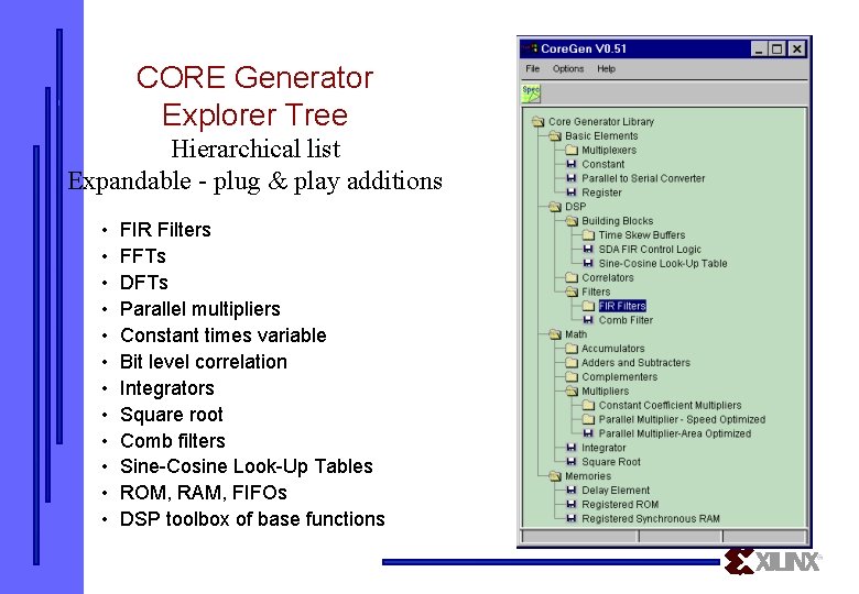
CORE Generator Explorer Tree Hierarchical list Expandable - plug & play additions • • • FIR Filters FFTs DFTs Parallel multipliers Constant times variable Bit level correlation Integrators Square root Comb filters Sine-Cosine Look-Up Tables ROM, RAM, FIFOs DSP toolbox of base functions

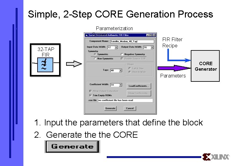
Simple, 2 -Step CORE Generation Process Parameterization Screen 32 -TAP FIR ~ ~ ~ FIR Filter Recipe CORE Generator Parameters 1. Input the parameters that define the block 2. Generate the CORE

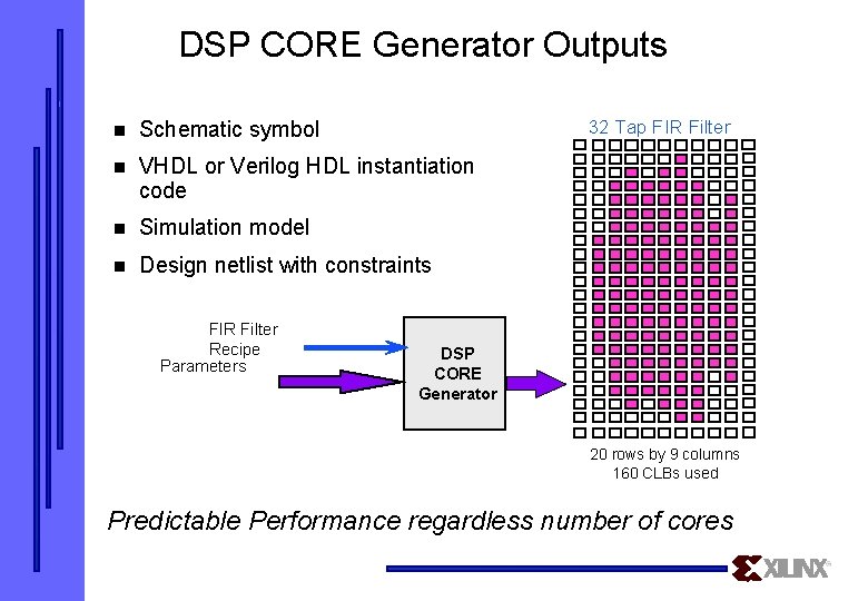
DSP CORE Generator Outputs n Schematic symbol n VHDL or Verilog HDL instantiation code n Simulation model n Design netlist with constraints FIR Filter Recipe Parameters 32 Tap FIR Filter DSP CORE Generator 20 rows by 9 columns 160 CLBs used Predictable Performance regardless number of cores

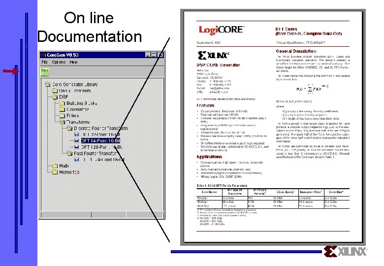
On line Documentation

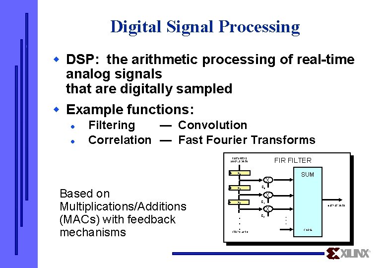
Digital Signal Processing w DSP: the arithmetic processing of real-time analog signals that are digitally sampled w Example functions: l l Filtering — Convolution Correlation — Fast Fourier Transforms FIR FILTER N BITS WIDE SAMPLE DATA SUM X 0 X • Based on Multiplications/Additions (MACs) with feedback mechanisms X 1 C 0 X • X 2 C 1 • • • K TAPS LONG OUTPUT DATA X • C 2 • • • K SUMs

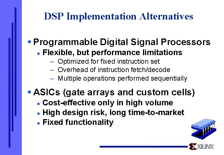
DSP Implementation Alternatives w Programmable Digital Signal Processors l Flexible, but performance limitations – Optimized for fixed instruction set – Overhead of instruction fetch/decode – Multiple operations performed sequentially w ASICs (gate arrays and custom cells) Cost-effective only in high volume l High design risk, long time-to-market l Fixed functionality l

FPGAs in DSP Applications FPGAs Are Cost-Effective for a Wide Variety of DSP Tasks w Versatility of programmable solution Configurable to specific needs l Encourages exploration of “algorithm space” l w Performance of dedicated hardware l Inherent parallelism w Algorithmic approach & design techniques must be suitable for FPGA architecture

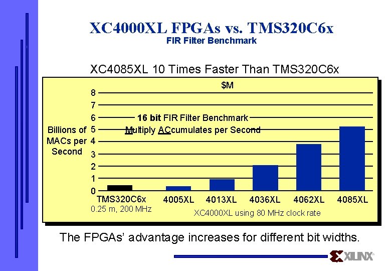
XC 4000 XL FPGAs vs. TMS 320 C 6 x FIR Filter Benchmark XC 4085 XL 10 Times Faster Than TMS 320 C 6 x 8 7 6 Billions of 5 MACs per 4 Second 3 2 1 0 $M 16 bit FIR Filter Benchmark Multiply ACcumulates per Second TMS 320 C 6 x 0. 25 m, 200 MHz 4005 XL 4013 XL 4036 XL 4062 XL 4085 XL XC 4000 XL using 80 MHz clock rate The FPGAs’ advantage increases for different bit widths.

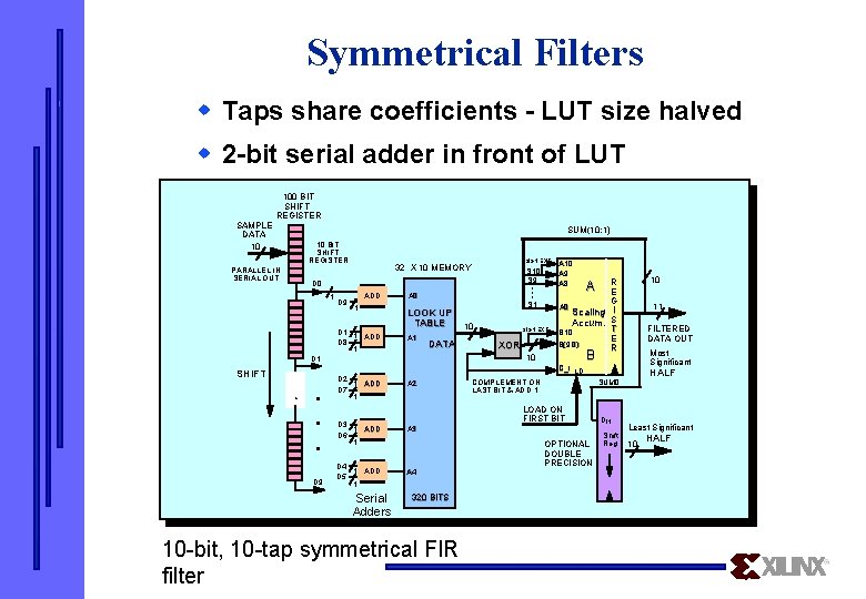
Symmetrical Filters w Taps share coefficients - LUT size halved w 2 -bit serial adder in front of LUT SAMPLE DATA 10 100 BIT SHIFT REGISTER SUM(10: 1) 10 BIT SHIFT REGISTER PARALLEL IN SERIAL OUT S 10 S 9 • • • S 1 D 0 1 D 9 ADD 1 1 ADD D 8 1 A 0 LOOK UP TABLE A 1 DATA • • • D 9 D 2 1 ADD D 7 1 D 3 1 ADD D 6 1 D 4 1 ADD D 5 1 Serial Adders 10 SIGN EXT XOR 10 D 1 SHIFT SIGN EXT 32 X 10 MEMORY A 10 A 9 A 8 10 R E G A 0 Scaling I Accum. S T B 10 E B(9: 0) R A 11 FILTERED DATA OUT Most Significant B C_I LD A 2 COMPLEMENT ON LAST BIT & ADD 1 LOAD ON FIRST BIT A 3 A 4 320 BITS 10 -bit, 10 -tap symmetrical FIR filter HALF SUM 0 OPTIONAL DOUBLE PRECISION DIN Shift Reg. Least Significant 10 HALF

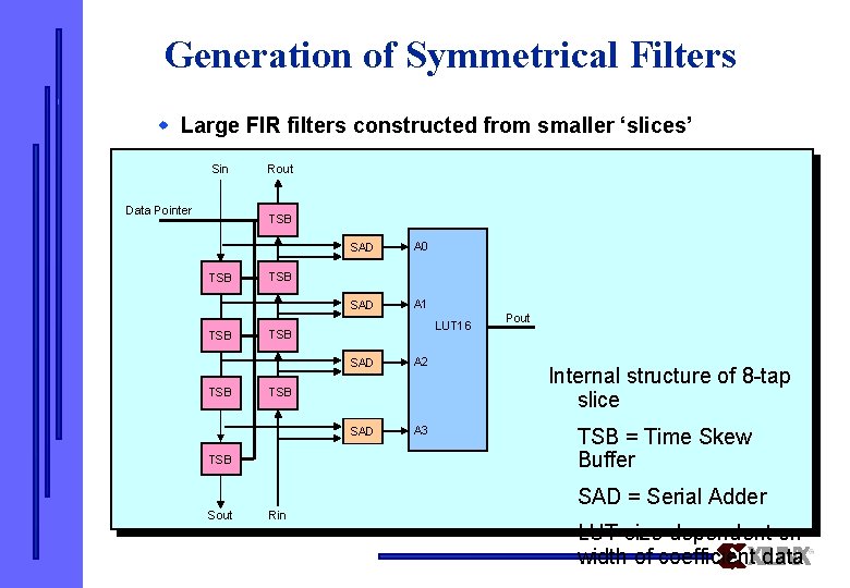
Generation of Symmetrical Filters w Large FIR filters constructed from smaller ‘slices’ Sin Data Pointer Rout TSB TSB SAD A 0 SAD A 1 TSB LUT 16 TSB SAD A 2 SAD A 3 TSB Pout Internal structure of 8 -tap slice TSB = Time Skew Buffer SAD = Serial Adder Sout Rin LUT size dependent on width of coefficient data

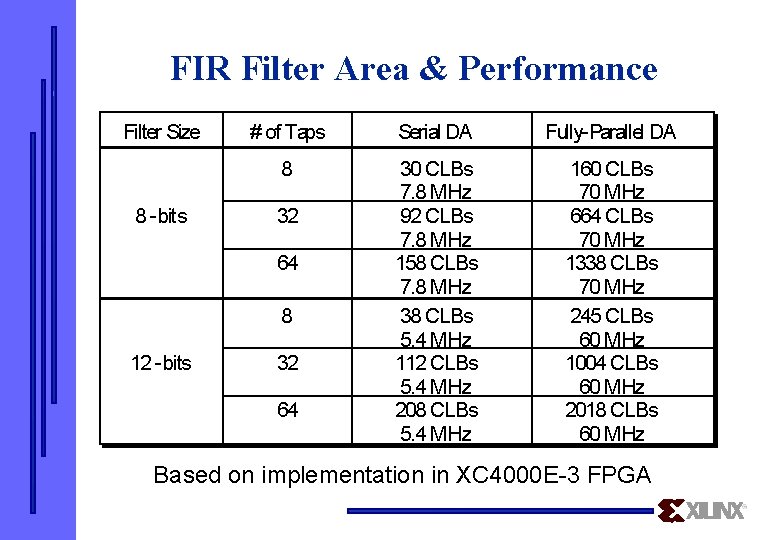
FIR Filter Area & Performance Filter Size 8 -bits # of Taps Serial DA Fully-Parallel DA 8 30 CLBs 7. 8 MHz 92 CLBs 7. 8 MHz 158 CLBs 7. 8 MHz 38 CLBs 5. 4 MHz 112 CLBs 5. 4 MHz 208 CLBs 5. 4 MHz 160 CLBs 70 MHz 664 CLBs 70 MHz 1338 CLBs 70 MHz 245 CLBs 60 MHz 1004 CLBs 60 MHz 2018 CLBs 60 MHz 32 64 8 12 -bits 32 64 Based on implementation in XC 4000 E-3 FPGA

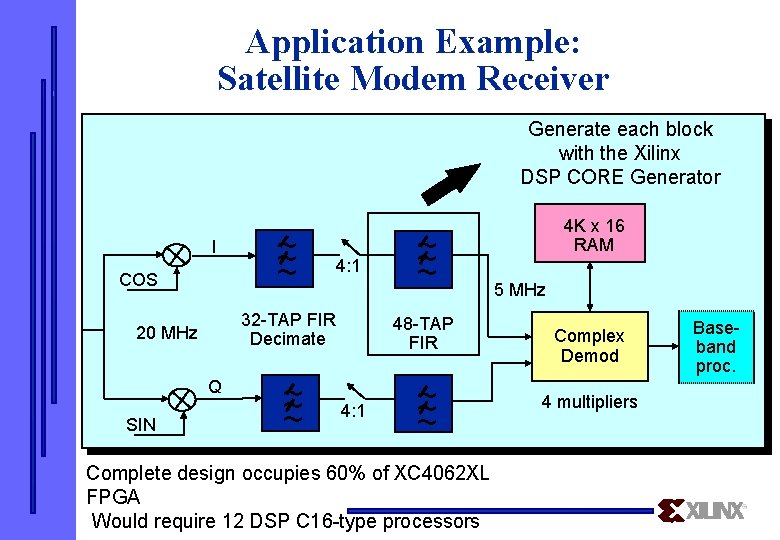
Application Example: Satellite Modem Receiver Generate each block with the Xilinx DSP CORE Generator I COS 4: 1 32 -TAP FIR Decimate 20 MHz Q SIN ~ ~ ~ ~ ~ 48 -TAP FIR 4: 1 ~ ~ ~ Complete design occupies 60% of XC 4062 XL FPGA Would require 12 DSP C 16 -type processors 4 K x 16 RAM 5 MHz Complex Demod 4 multipliers Baseband proc.

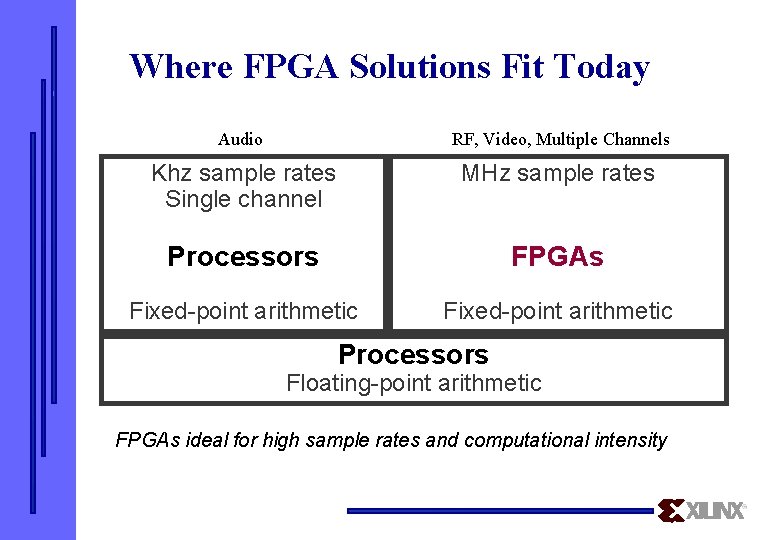
Where FPGA Solutions Fit Today Audio RF, Video, Multiple Channels Khz sample rates Single channel MHz sample rates Processors FPGAs Fixed-point arithmetic Processors Floating-point arithmetic FPGAs ideal for high sample rates and computational intensity

Logi. Core PCI Interface

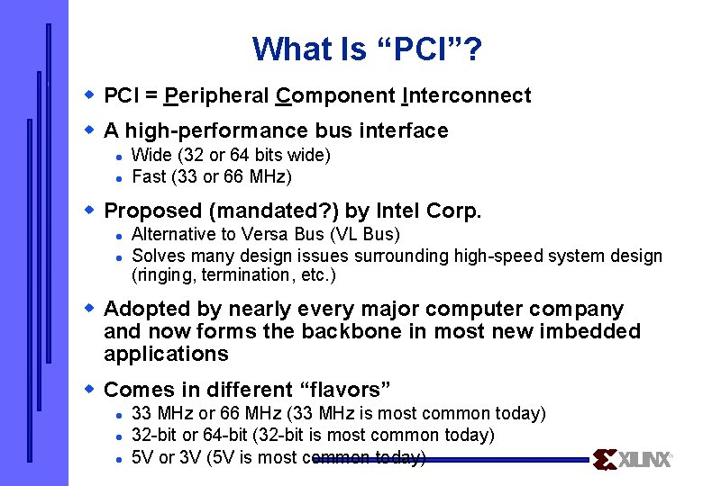
What Is “PCI”? w PCI = Peripheral Component Interconnect w A high-performance bus interface l l Wide (32 or 64 bits wide) Fast (33 or 66 MHz) w Proposed (mandated? ) by Intel Corp. l l Alternative to Versa Bus (VL Bus) Solves many design issues surrounding high-speed system design (ringing, termination, etc. ) w Adopted by nearly every major computer company and now forms the backbone in most new imbedded applications w Comes in different “flavors” l l l 33 MHz or 66 MHz (33 MHz is most common today) 32 -bit or 64 -bit (32 -bit is most common today) 5 V or 3 V (5 V is most common today)

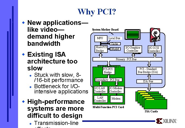
Why PCI? w New applications— like video— demand higher bandwidth w Existing ISA architecture too slow l l Stuck with slow, 8/16 -bit performance Bottleneck for I/Ointensive applications w High-performance systems are more difficult to design l Transmission-line System Mother Board MPU Host-PCI Bridge Local Bus Cache DRAM I/O Graphics Controller I/O SCSI Controller Primary PCI Bus PCI-PCI Bridge PCI - Standard Bus Bridge (ISA) Secondary PCI Bus ISA Bus I/O LAN Controller I/O Modem Controller LAN Controller Modem Multi-Function PCI Card ISA Cards

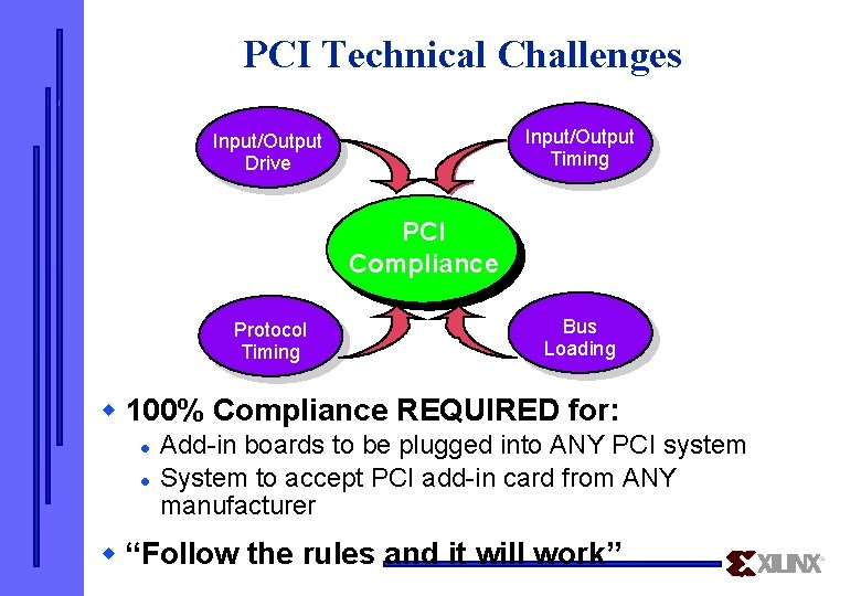
PCI Technical Challenges Input/Output Timing Input/Output Drive PCI Compliance Protocol Timing Bus Loading w 100% Compliance REQUIRED for: l l Add-in boards to be plugged into ANY PCI system System to accept PCI add-in card from ANY manufacturer w “Follow the rules and it will work”

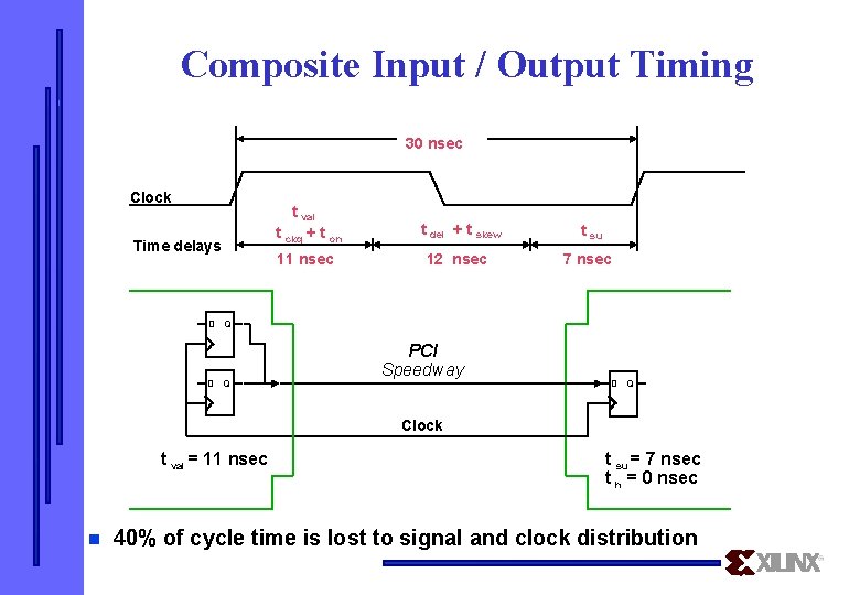
Composite Input / Output Timing 30 nsec Clock Time delays t val t ckq + t on t del + t skew t su 11 nsec 12 nsec 7 nsec D Q PCI Speedway D Q Clock t val = 11 nsec n t su = 7 nsec t h = 0 nsec 40% of cycle time is lost to signal and clock distribution

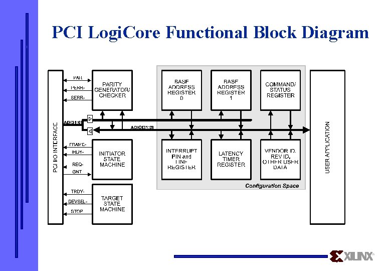
PCI Logi. Core Functional Block Diagram

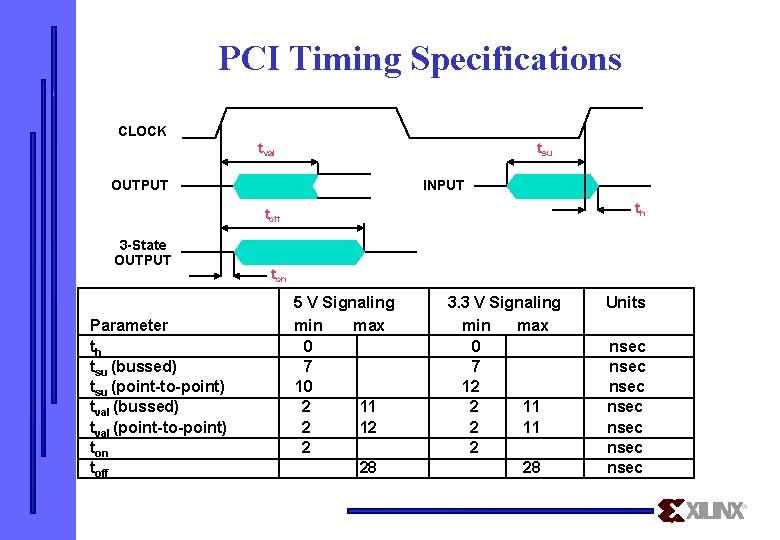
PCI Timing Specifications CLOCK tval tsu OUTPUT INPUT th toff 3 -State OUTPUT Parameter th tsu (bussed) tsu (point-to-point) tval (bussed) tval (point-to-point) ton toff ton 5 V Signaling min max 0 7 10 2 11 2 12 2 28 3. 3 V Signaling min max 0 7 12 2 11 2 28 Units nsec nsec

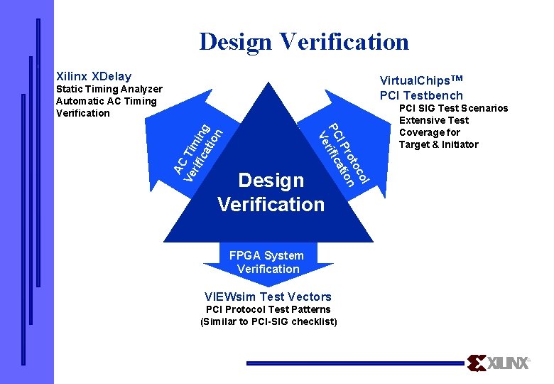
Design Verification Xilinx XDelay Virtual. Chips. TM PCI Testbench Static Timing Analyzer Automatic AC Timing Verification AC Ve Tim rif ica ing tio n ol toc ro on I P ati PC rific Ve Design Verification FPGA System Verification VIEWsim Test Vectors PCI Protocol Test Patterns (Similar to PCI-SIG checklist) PCI SIG Test Scenarios Extensive Test Coverage for Target & Initiator

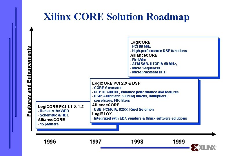
Xilinx CORE Solution Roadmap Features and Enhancements Logi. CORE - PCI 66 MHz - High-performance DSP functions Alliance. CORE - Fire. Wire - ATM SAR, UTOPIA 50 MHz, - Micro Sequencer - Microprocessor I/Fs Logi. CORE PCI 2. 0 & DSP - CORE Generator - PCI: XC 4000 XL, enhance performance and features - DSP: Arithmetic building blocks, multipliers, correlators, FIR filters Logi. CORE PCI 1. 1 & 1. 2 Alliance. CORE - Runs on the WEB - Schematic & HDL Logi. BLOX Alliance. CORE - USB, PCMCIA, 82 XX, Reed-Solomon - Integrated with EDA vendors & Xilinx software solutions - 15 partners 1996 1997 1998 1999


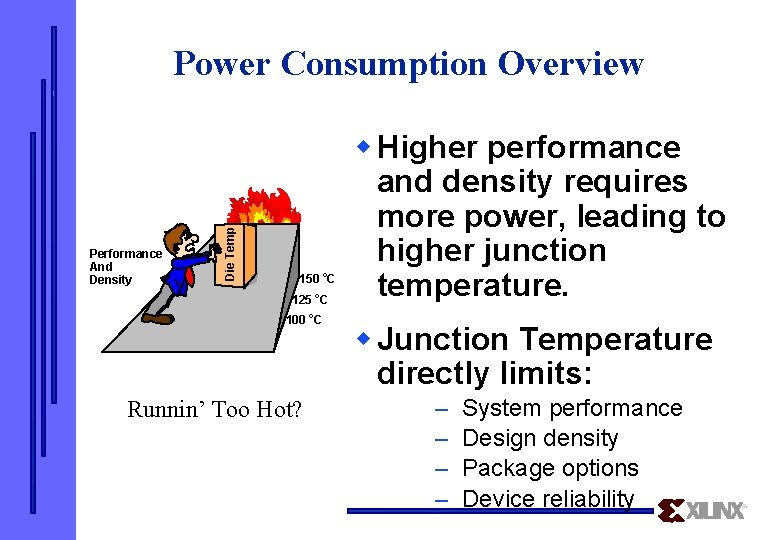
Performance And Density Die Temp Power Consumption Overview 150 o. C 125 o. C 100 o. C Runnin’ Too Hot? w Higher performance and density requires more power, leading to higher junction temperature. w Junction Temperature directly limits: – – System performance Design density Package options Device reliability

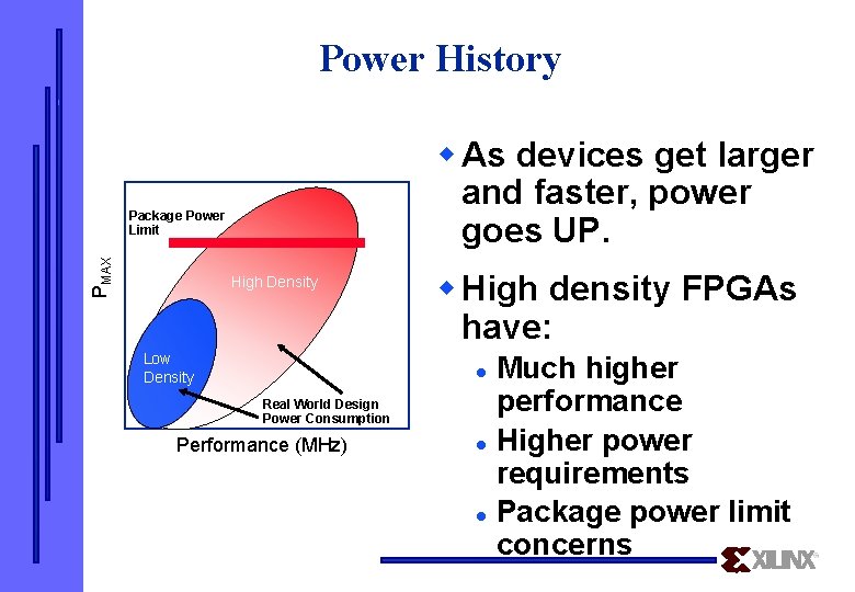
Power History w As devices get larger and faster, power goes UP. PMAX Package Power Limit High Density Low Density w High density FPGAs have: Much higher performance l Higher power requirements l Package power limit concerns l Real World Design Power Consumption Performance (MHz)

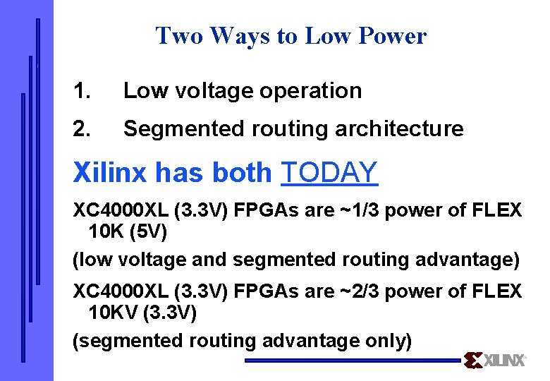
Two Ways to Low Power 1. Low voltage operation 2. Segmented routing architecture Xilinx has both TODAY XC 4000 XL (3. 3 V) FPGAs are ~1/3 power of FLEX 10 K (5 V) (low voltage and segmented routing advantage) XC 4000 XL (3. 3 V) FPGAs are ~2/3 power of FLEX 10 KV (3. 3 V) (segmented routing advantage only)

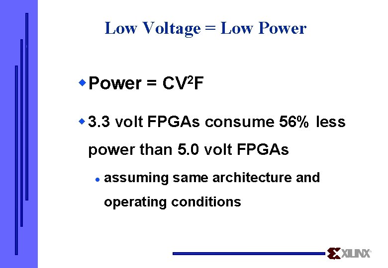
Low Voltage = Low Power = CV 2 F w 3. 3 volt FPGAs consume 56% less power than 5. 0 volt FPGAs l assuming same architecture and operating conditions

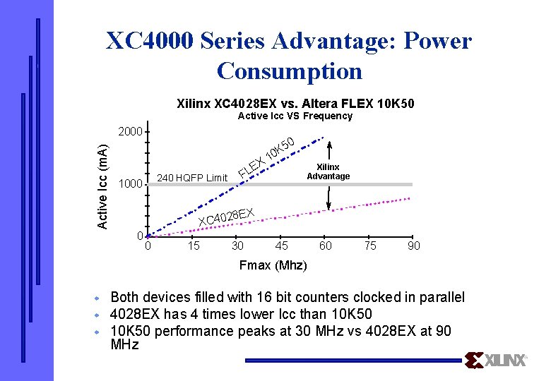
XC 4000 Series Advantage: Power Consumption Xilinx XC 4028 EX vs. Altera FLEX 10 K 50 Active Icc VS Frequency Active Icc (m. A) 2000 240 HQFP Limit 1000 EX L F 50 K 0 1 Xilinx Advantage X 8 E XC 402 0 0 15 30 45 60 75 90 Fmax (Mhz) w w w Both devices filled with 16 bit counters clocked in parallel 4028 EX has 4 times lower Icc than 10 K 50 performance peaks at 30 MHz vs 4028 EX at 90 MHz

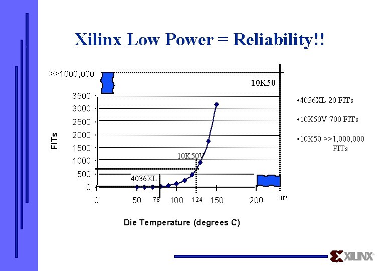
Xilinx Low Power = Reliability!! >>1000, 000 10 K 50 3500 • 4036 XL 20 FITs 3000 2500 • 10 K 50 V 700 FITs 2000 • 10 K 50 >>1, 000 FITs 1500 10 K 50 V 1000 500 4036 XL 0 0 50 78 100 124 150 Die Temperature (degrees C) 200 302

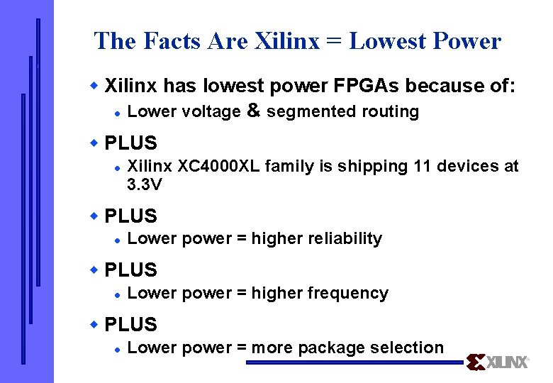
The Facts Are Xilinx = Lowest Power w Xilinx has lowest power FPGAs because of: l Lower voltage & segmented routing w PLUS l Xilinx XC 4000 XL family is shipping 11 devices at 3. 3 V w PLUS l Lower power = higher reliability w PLUS l Lower power = higher frequency w PLUS l Lower power = more package selection

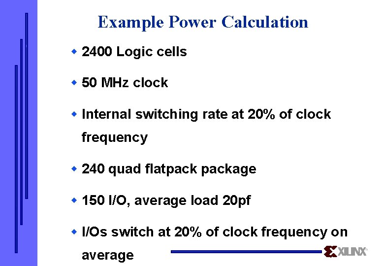
Example Power Calculation w 2400 Logic cells w 50 MHz clock w Internal switching rate at 20% of clock frequency w 240 quad flatpackage w 150 I/O, average load 20 pf w I/Os switch at 20% of clock frequency on average

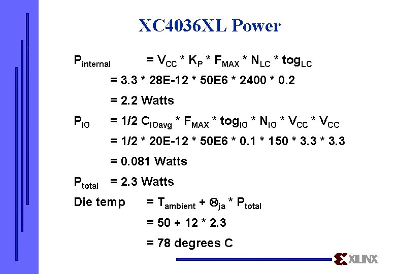
XC 4036 XL Power Pinternal = VCC * KP * FMAX * NLC * tog. LC = 3. 3 * 28 E-12 * 50 E 6 * 2400 * 0. 2 = 2. 2 Watts PIO = 1/2 CIOavg * FMAX * tog. IO * NIO * VCC = 1/2 * 20 E-12 * 50 E 6 * 0. 1 * 150 * 3. 3 = 0. 081 Watts Ptotal = 2. 3 Watts Die temp = Tambient + Qja * Ptotal = 50 + 12 * 2. 3 = 78 degrees C

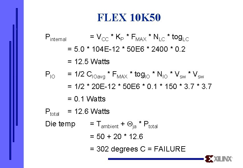
FLEX 10 K 50 Pinternal = VCC * KP * FMAX * NLC * tog. LC = 5. 0 * 104 E-12 * 50 E 6 * 2400 * 0. 2 = 12. 5 Watts PIO = 1/2 CIOavg * FMAX * tog. IO * NIO * Vsw = 1/2 * 20 E-12 * 50 E 6 * 0. 1 * 150 * 3. 7 = 0. 1 Watts Ptotal = 12. 6 Watts Die temp = Tambient + Qja * Ptotal = 50 + 20 * 12. 6 = 302 degrees C = FAILURE

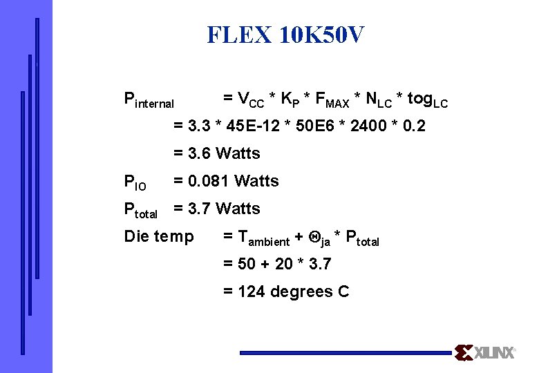
FLEX 10 K 50 V Pinternal = VCC * KP * FMAX * NLC * tog. LC = 3. 3 * 45 E-12 * 50 E 6 * 2400 * 0. 2 = 3. 6 Watts PIO = 0. 081 Watts Ptotal = 3. 7 Watts Die temp = Tambient + Qja * Ptotal = 50 + 20 * 3. 7 = 124 degrees C