The Xilinx Virtex Series FPGA Virtex FPGA Structure

- Slides: 34

The Xilinx Virtex Series FPGA • Virtex FPGA Structure • Specific Features – IOB – CLB - Function Generators, Flip-Flops, SRAM, and Fast Carry Logic – Three-State Buffers – Block Select. RAM – Programmable Routing Matrix – Clock Distribution (Delay-Locked Loops) – Boundary Scan – Configuration • Virtex XCV 800 -PQ/HQ 240 C Characteristics 11/25/2020 ECE 554 1

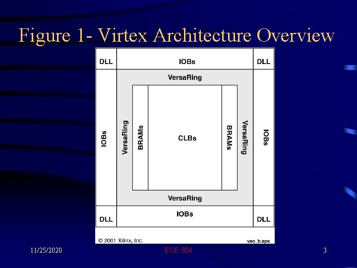
Virtex FPGA Architecture • Primary Reference: – On-Line Xilinx Data Sheet DS 003 (v. 2. 5, April 2, 2001) - http: //www. xilinx. com/partinfo/ds 003. pdf • See Figure 1: Virtex Architecture Overview – – – – IOBs - Input/Output Blocks CLBs - Configurable Logic Blocks GRM - General Routing Matrix 3 -state buffers BRAMs - Block Select. RAM DLLs - Delay-Locked Loops Versa. Ring - I/O interface routing resources 11/25/2020 ECE 554 2

Figure 1 - Virtex Architecture Overview 11/25/2020 ECE 554 3

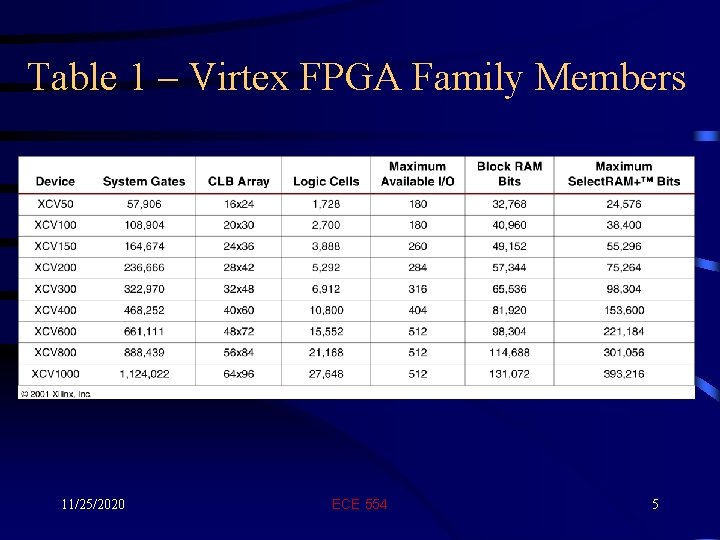
Virtex FPGA Architecture • Logic configured by values stored in SRAM cells – CLBs implement logic in SRAM-stored truth tables – CLBs use SRAM-controlled multiplexers – Routing uses “pass” transistors for making/breaking connections between wire segments • See Table 1: Virtex FPGA Family Members 11/25/2020 ECE 554 4

Table 1 – Virtex FPGA Family Members 11/25/2020 ECE 554 5

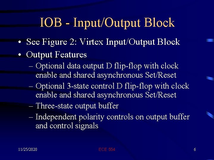
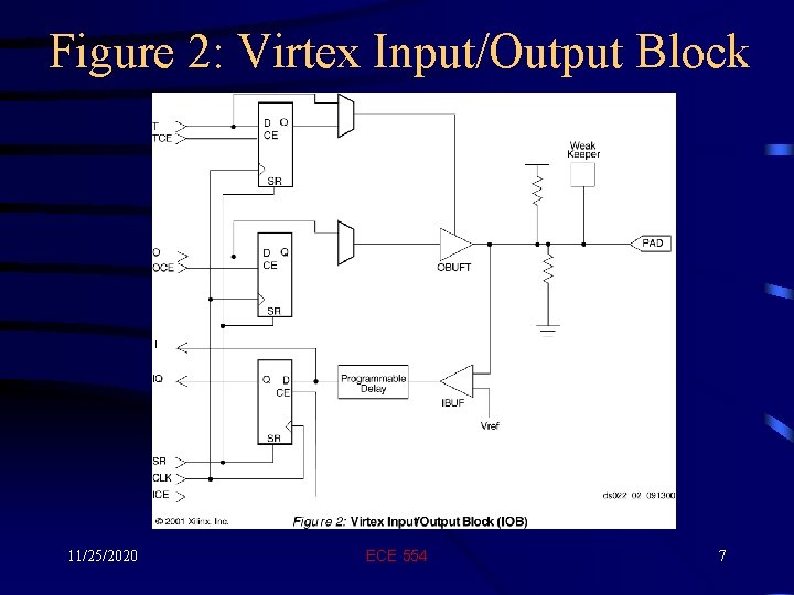
IOB - Input/Output Block • See Figure 2: Virtex Input/Output Block • Output Features – Optional data output D flip-flop with clock enable and shared asynchronous Set/Reset – Optional 3 -state control D flip-flop with clock enable and shared asynchronous Set/Reset – Three-state output buffer – Independent polarity controls on output buffer and control signals 11/25/2020 ECE 554 6

Figure 2: Virtex Input/Output Block 11/25/2020 ECE 554 7

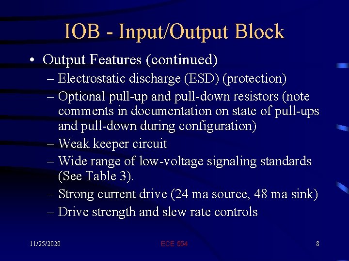
IOB - Input/Output Block • Output Features (continued) – Electrostatic discharge (ESD) (protection) – Optional pull-up and pull-down resistors (note comments in documentation on state of pull-ups and pull-down during configuration) – Weak keeper circuit – Wide range of low-voltage signaling standards (See Table 3). – Strong current drive (24 ma source, 48 ma sink) – Drive strength and slew rate controls 11/25/2020 ECE 554 8

IOB - Input/Output Block • Input Features – Input Buffer – Wide range of low-voltage signaling standards – Programmable delay forcing pad-to-pad hold time to zero – Optional data D flip-flop with clock enable and shared Set/Reset – Optional pull-up and pull-down resistors (Same ones as for output use) 11/25/2020 ECE 554 9

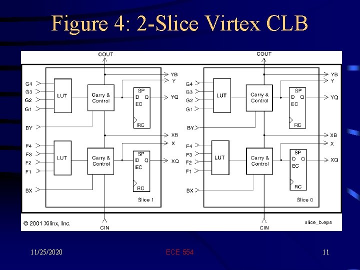
CLB - Configurable Logic Block • See Figure 4: 2 -Slice Virtex CLB • Contains two logic cells • Each logic cell contains: – 2 Look-up tables (LUTs) – 2 D flip-flops/latches – Fast carry logic – Three-state drivers – SRAM control logic 11/25/2020 ECE 554 10

Figure 4: 2 -Slice Virtex CLB 11/25/2020 ECE 554 11

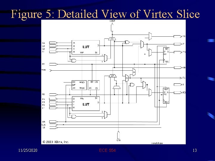
CLB - Configurable Logic Block • See Figure 5: Detailed View of Virtex Slice • Logic Function Implementation – 2 Function Generators - Each a 4 -input LUT implements any 4 -input function – F 5 multiplexer - combines two LUTs with select input implements any 5 -input function, 4 -to-1 mux, or selected functions of up to 9 inputs. – F 6 multiplexer - combines outputs of two F 5 multiplexer - implements any 6 -input function, 8 -to-1 mux, or selected functions of up to 19 inputs. – Four direct feedthrough paths - useful to facilitate routing by use of through-the-cell paths 11/25/2020 ECE 554 12

Figure 5: Detailed View of Virtex Slice 11/25/2020 ECE 554 13

CLB - Configurable Logic Block • Storage Elements – – 2 D flip-flops/latches Optionally included in cell output paths Shared clock enable Shared synchronous/asynchronous Set/Reset signals • SR - forces storage element into initialization state specified • BY - forces storage element into opposite state – All control signals independently invertible 11/25/2020 ECE 554 14

CLB - Configurable Logic Block • Fast Carry Logic (See Figure 5) – Two chains of two bits per CLB – AND gate, 0/1 Mux, CY Mux, EXOR – Manchester Carry Chain-Like • 3 -state Drivers (BUFT) - on-chip drivers with independent control (T and E) and input pins • Distributed LUT Select. RAMs - Per logic cell, one of: • • • 11/25/2020 Two 16 x 1 -bit synchronous RAM 16 x 2 -bit synchronous RAM 32 x 1 -bit synchronous RAM 16 x 1 dual-port synchronous RAM Two 16 -bit shift registers ECE 554 15

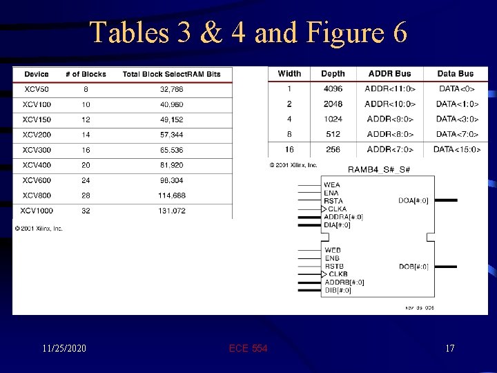
Block Select. RAM • Fully synchronous dual-ported 4096 -bit RAM – – Stores address, data and write-control signal on inputs Cannot change address, even for read without using clock For dual port use, interesting timing restrictions See App Note XAPP 130 http: //www. xilinx. com/xapp 130. pdf • Organized in vertical columns of blocks on left and right of CLB array • Block height is 4 CLBs => Number of block per column is (height of CLB of array)/4 • See Table 3: Virtex Block Select. RAM Amounts • See Figure 6: Dual-Port Block Select. RAM • Independent control signals for each port • See Table 4: Block Select. RAM Port Aspect Ratios • Ratios independently selectable 11/25/2020 ECE 554 16

Tables 3 & 4 and Figure 6 11/25/2020 ECE 554 17

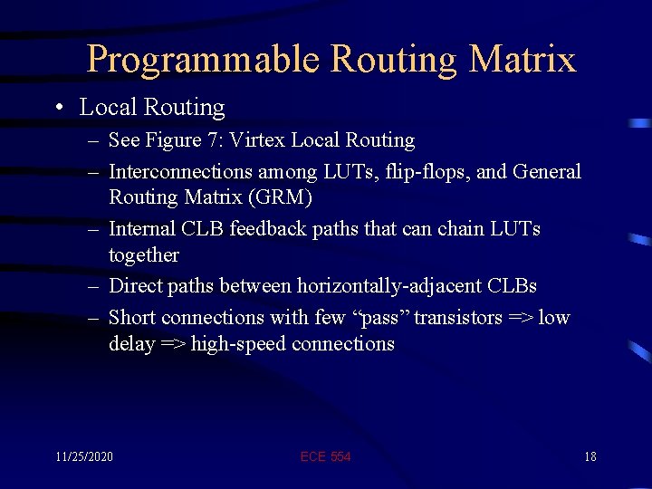
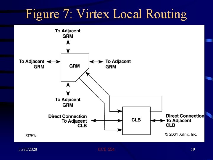
Programmable Routing Matrix • Local Routing – See Figure 7: Virtex Local Routing – Interconnections among LUTs, flip-flops, and General Routing Matrix (GRM) – Internal CLB feedback paths that can chain LUTs together – Direct paths between horizontally-adjacent CLBs – Short connections with few “pass” transistors => low delay => high-speed connections 11/25/2020 ECE 554 18

Figure 7: Virtex Local Routing 11/25/2020 ECE 554 19

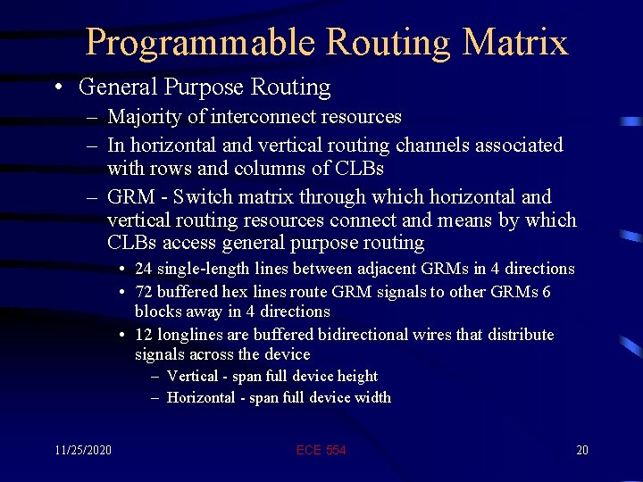
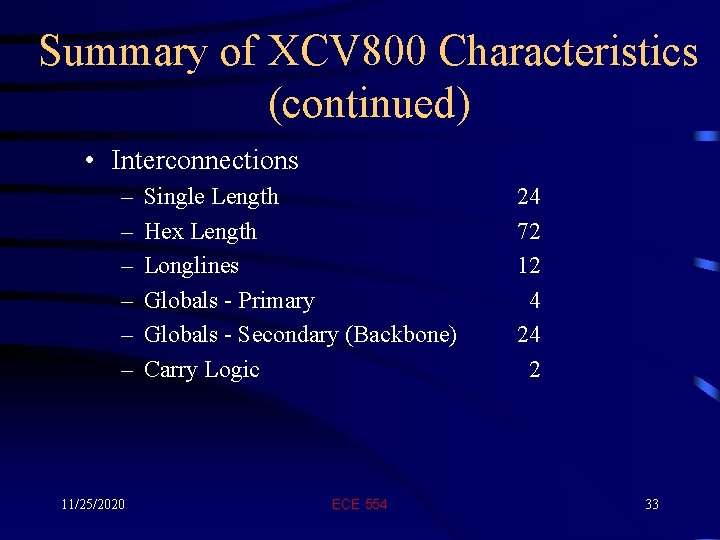
Programmable Routing Matrix • General Purpose Routing – Majority of interconnect resources – In horizontal and vertical routing channels associated with rows and columns of CLBs – GRM - Switch matrix through which horizontal and vertical routing resources connect and means by which CLBs access general purpose routing • 24 single-length lines between adjacent GRMs in 4 directions • 72 buffered hex lines route GRM signals to other GRMs 6 blocks away in 4 directions • 12 longlines are buffered bidirectional wires that distribute signals across the device – Vertical - span full device height – Horizontal - span full device width 11/25/2020 ECE 554 20

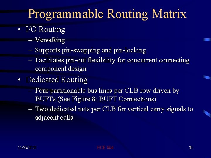
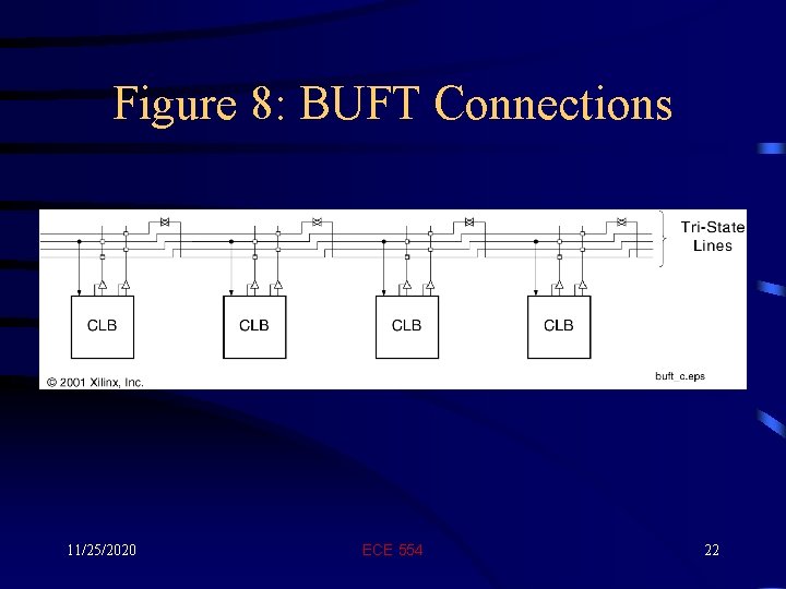
Programmable Routing Matrix • I/O Routing – Versa. Ring – Supports pin-swapping and pin-locking – Facilitates pin-out flexibility for concurrent connecting component design • Dedicated Routing – Four partitionable bus lines per CLB row driven by BUFTs (See Figure 8: BUFT Connections) – Two dedicated nets per CLB for vertical carry signals to adjacent cells 11/25/2020 ECE 554 21

Figure 8: BUFT Connections 11/25/2020 ECE 554 22

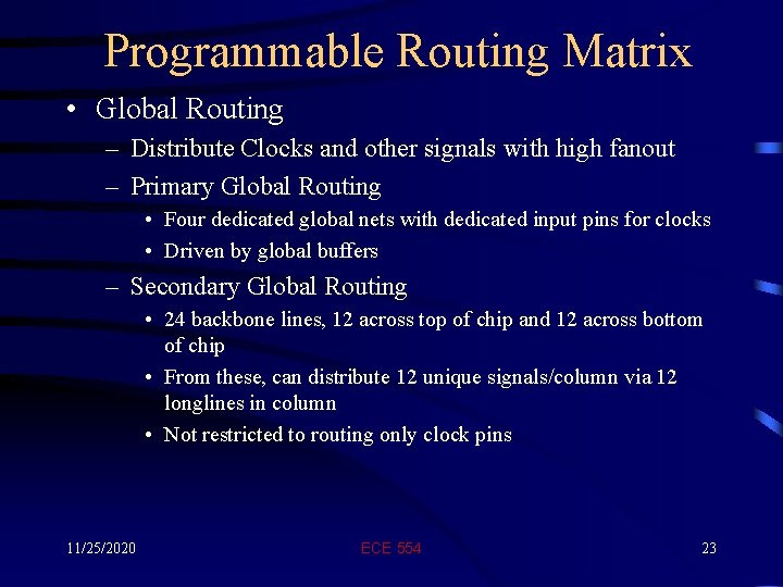
Programmable Routing Matrix • Global Routing – Distribute Clocks and other signals with high fanout – Primary Global Routing • Four dedicated global nets with dedicated input pins for clocks • Driven by global buffers – Secondary Global Routing • 24 backbone lines, 12 across top of chip and 12 across bottom of chip • From these, can distribute 12 unique signals/column via 12 longlines in column • Not restricted to routing only clock pins 11/25/2020 ECE 554 23

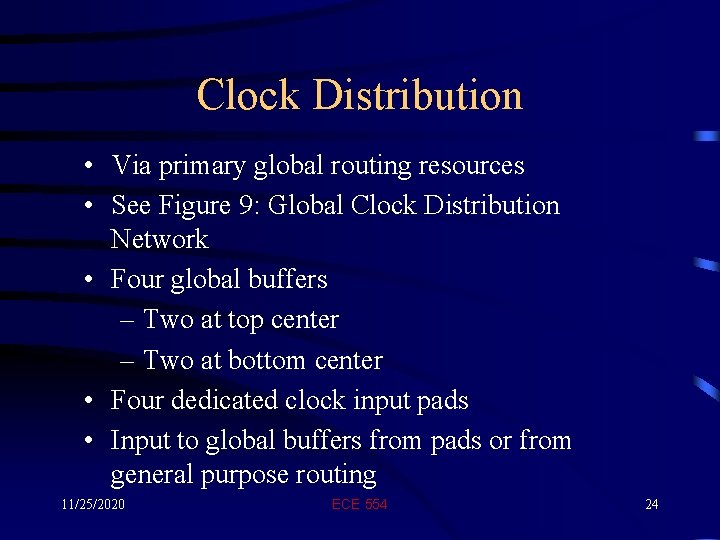
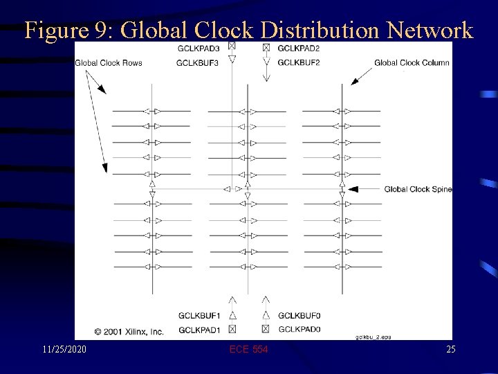
Clock Distribution • Via primary global routing resources • See Figure 9: Global Clock Distribution Network • Four global buffers – Two at top center – Two at bottom center • Four dedicated clock input pads • Input to global buffers from pads or from general purpose routing 11/25/2020 ECE 554 24

Figure 9: Global Clock Distribution Network 11/25/2020 ECE 554 25

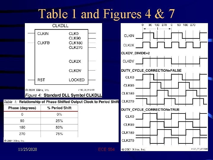
Delay-Locked Loops (DLLs) • One associated with each clock buffer • Eliminate skew between clock input and internal clock-input pins within the device • Each can drive two global clock networks • Clock edges reach internal flip-flops 1 to 4 clock periods after they arrive at the input. • Provides control of multiple clock domains (See Tables 1 and Figures 4 & 7 for DLL app note XAPP 132) • Has minimum clock frequency restrictions! 11/25/2020 ECE 554 26

Table 1 and Figures 4 & 7 11/25/2020 ECE 554 27

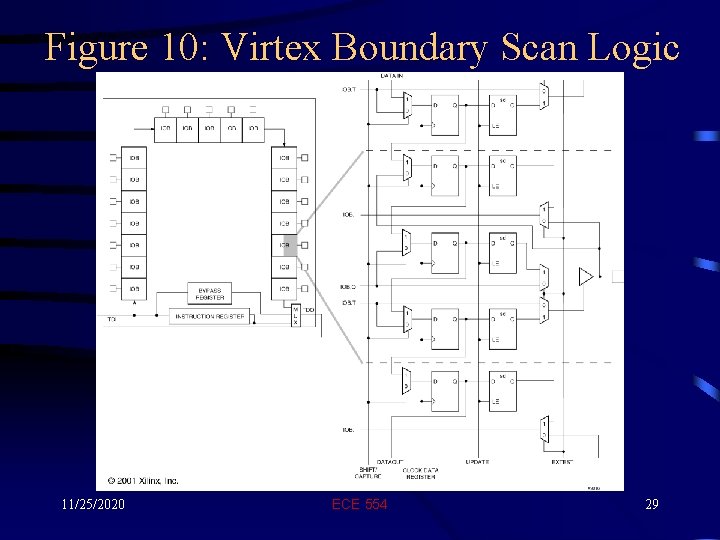
Boundary Scan • • IEEE(ANSI) Standard 1149. 1 Provides Ability to Observe and Control I/Os Accessed Through a Standard Test Access Port (TAP) TAP Has Four Inputs (TCK, TMS, TDI) and One Output (TDO) • Additional Logic Includes Test Instruction Register, ID Register, two User Registers and a One Bit Bypass Register. • Uses: – – Test Interconnects between ICs on Boards Perform Tests on Internal Logic Initial Built-In Self-Test Logic Perform Sampling During Normal Operation • See Figure 10: Virtex Series Boundary Scan Logic 11/25/2020 ECE 554 28

Figure 10: Virtex Boundary Scan Logic 11/25/2020 ECE 554 29

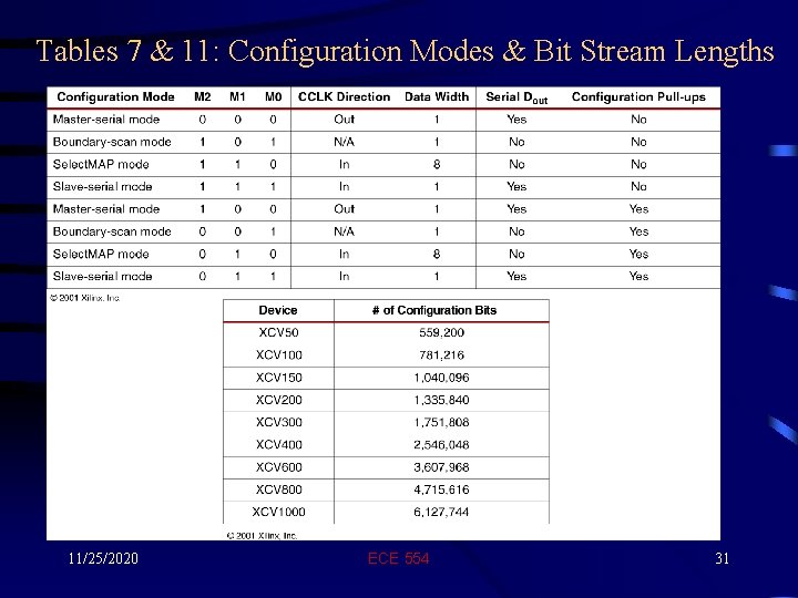
Configuration - How Is It Implemented? • Implemented by loading configuration data into 2 D configuration SRAM • See Table 7: Configuration Modes – Mode selected by Mode Pins - Dedicated pins, M 0, M 1, and M 2 for configuration • See Table 11: Virtex Bit Stream Lengths 11/25/2020 ECE 554 30

Tables 7 & 11: Configuration Modes & Bit Stream Lengths 11/25/2020 ECE 554 31

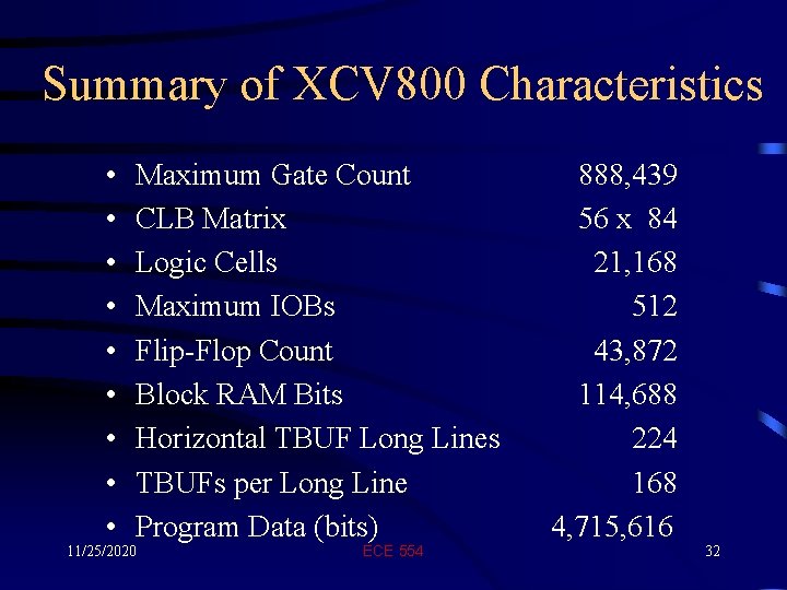
Summary of XCV 800 Characteristics • • • Maximum Gate Count CLB Matrix Logic Cells Maximum IOBs Flip-Flop Count Block RAM Bits Horizontal TBUF Long Lines TBUFs per Long Line Program Data (bits) 11/25/2020 ECE 554 888, 439 56 x 84 21, 168 512 43, 872 114, 688 224 168 4, 715, 616 32

Summary of XCV 800 Characteristics (continued) • Interconnections – – – 11/25/2020 Single Length Hex Length Longlines Globals - Primary Globals - Secondary (Backbone) Carry Logic ECE 554 24 72 12 4 24 2 33

References • On-Line Xilinx Data Sheet DS 003 (v. 2. 5, April 2, 2001) – http: //www. xilinx. com/partinfo/ds 003. pdf • XAPP 130 Using the Virtex Block Select. RAM+ Features (v 1. 4) – http: //www. xilinx. com/xapp 130. pdf • XAPP 132 Using the Virtex Delay-Locked Loop (v 2. 6) – http: //www. xilinx. com/xapp 132. pdf 11/25/2020 ECE 554 34