Lecture 11 Xilinx FPGA Memories ECE 448 FPGA




![Dual-Port Block RAM [p. A 1: 0] [p. B 1: 0] 18 Dual-Port Block RAM [p. A 1: 0] [p. B 1: 0] 18](https://slidetodoc.com/presentation_image_h/d33af5fb6133af49cbc92ccccc873108/image-18.jpg)







- Slides: 53

Lecture 11 Xilinx FPGA Memories ECE 448 – FPGA and ASIC Design with VHDL

Required reading • P. Chu, FPGA Prototyping by VHDL Examples Chapter 11, Xilinx Spartan-3 Specific Memory ECE 448 – FPGA and ASIC Design with VHDL 2

Recommended reading • XAPP 463 Using Block RAM in Spartan-3 Generation FPGAs Google search: XAPP 463 • XAPP 464 Using Look-Up Tables as Distributed RAM in Spartan-3 Generation FPGAs Google search: XAPP 464 • XST User Guide, Section: RAMs and ROMs HDL Coding Techniques Google search: XST User Guide (PDF) • ISE In-Depth Tutorial, Section: Creating a CORE Generator Software Module Google search: ISE In-Depth Tutorial ECE 448 – FPGA and ASIC Design with VHDL 3

Memory Types 4

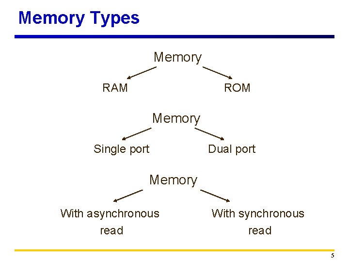
Memory Types Memory RAM ROM Memory Single port Dual port Memory With asynchronous read With synchronous read 5

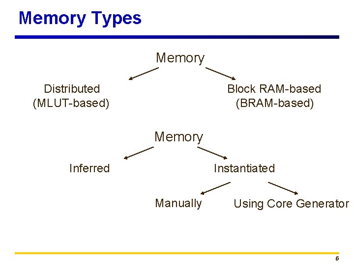
Memory Types Memory Distributed (MLUT-based) Block RAM-based (BRAM-based) Memory Inferred Instantiated Manually Using Core Generator 6

FPGA Distributed Memory 7

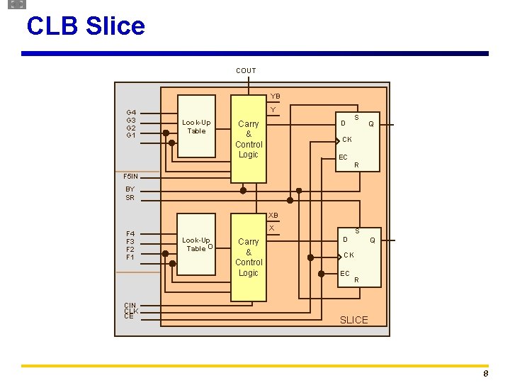
CLB Slice COUT YB G 4 G 3 G 2 G 1 Y Look-Up O Table D Carry & Control Logic S Q CK EC R F 5 IN BY SR XB F 4 F 3 F 2 F 1 CIN CLK CE X Look-Up Table O Carry & Control Logic S D Q CK EC R SLICE 8

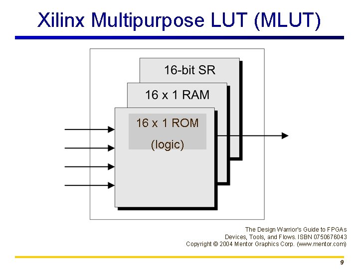
Xilinx Multipurpose LUT (MLUT) 16 x 1 ROM (logic) The Design Warrior’s Guide to FPGAs Devices, Tools, and Flows. ISBN 0750676043 Copyright © 2004 Mentor Graphics Corp. (www. mentor. com) 9

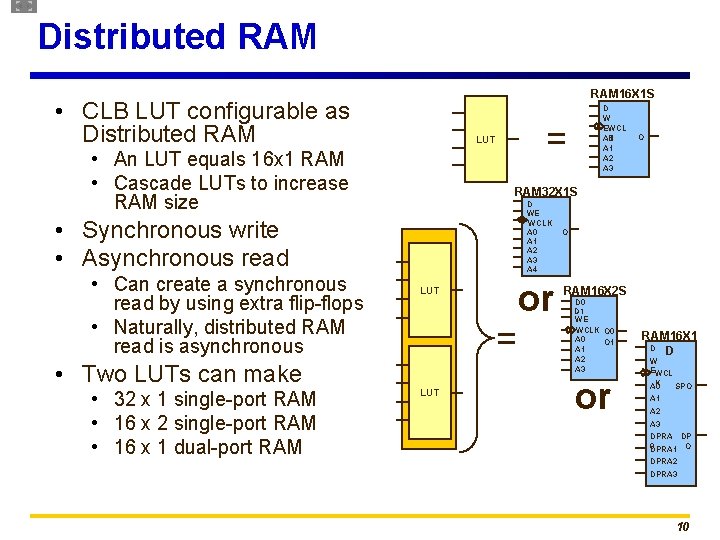
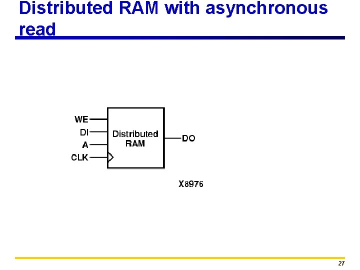
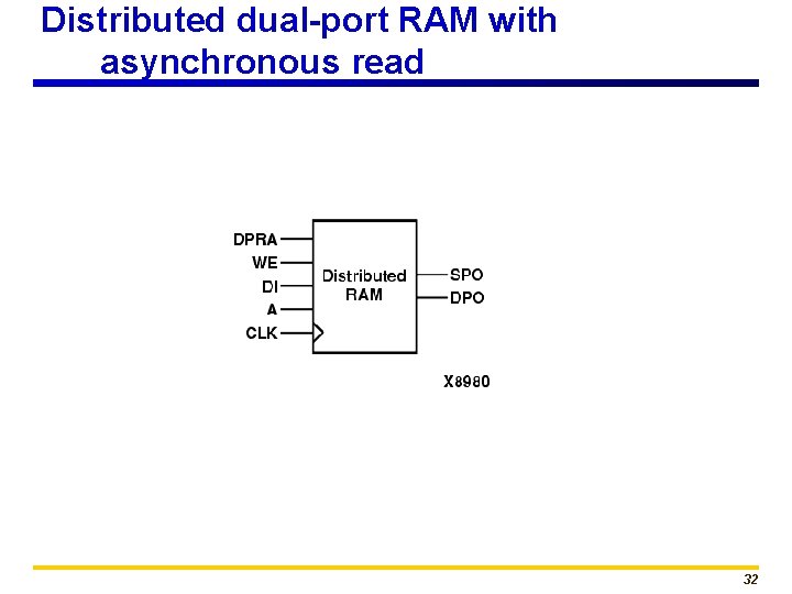
Distributed RAM 16 X 1 S • CLB LUT configurable as Distributed RAM = LUT • An LUT equals 16 x 1 RAM • Cascade LUTs to increase RAM size D WE WCLK A 0 A 1 A 2 A 3 A 4 LUT = • Two LUTs can make • 32 x 1 single-port RAM • 16 x 2 single-port RAM • 16 x 1 dual-port RAM O RAM 32 X 1 S • Synchronous write • Asynchronous read • Can create a synchronous read by using extra flip-flops • Naturally, distributed RAM read is asynchronous D W EWCL K A 0 A 1 A 2 A 3 LUT or O RAM 16 X 2 S D 0 D 1 WE WCLK O 0 A 0 O 1 A 2 A 3 or RAM 16 X 1 D D W EWCL K A 0 SPO A 1 A 2 A 3 DPRA DP 0 DPRA 1 O DPRA 2 DPRA 3 10

FPGA Block RAM 11

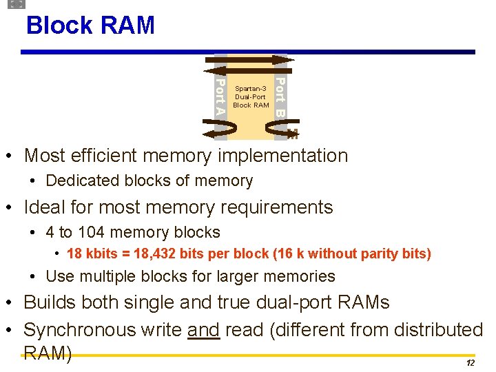
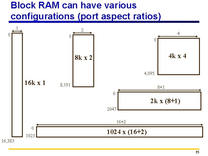
Block RAM Port B Port A Spartan-3 Dual-Port Block RAM • Most efficient memory implementation • Dedicated blocks of memory • Ideal for most memory requirements • 4 to 104 memory blocks • 18 kbits = 18, 432 bits per block (16 k without parity bits) • Use multiple blocks for larger memories • Builds both single and true dual-port RAMs • Synchronous write and read (different from distributed RAM) 12

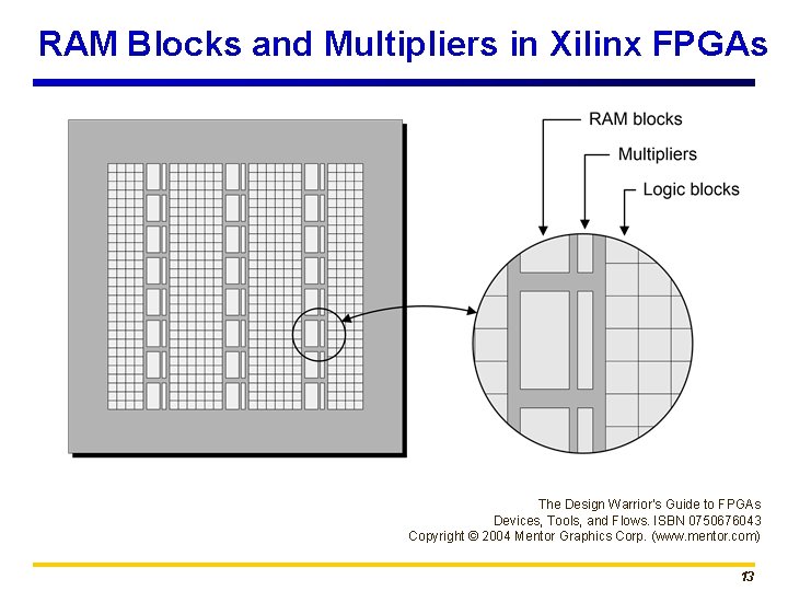
RAM Blocks and Multipliers in Xilinx FPGAs The Design Warrior’s Guide to FPGAs Devices, Tools, and Flows. ISBN 0750676043 Copyright © 2004 Mentor Graphics Corp. (www. mentor. com) 13

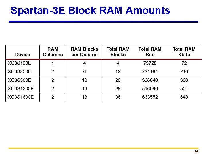
Spartan-3 E Block RAM Amounts 14

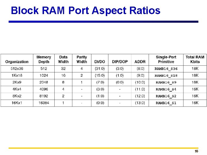
Block RAM can have various configurations (port aspect ratios) 1 2 0 4 0 0 4 k x 4 8 k x 2 4, 095 16 k x 1 8, 191 8+1 0 2 k x (8+1) 2047 16+2 0 1023 1024 x (16+2) 16, 383 15

Block RAM Port Aspect Ratios 16

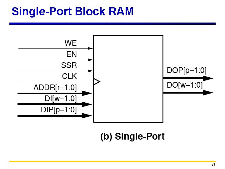
Single-Port Block RAM 17
![DualPort Block RAM p A 1 0 p B 1 0 18 Dual-Port Block RAM [p. A 1: 0] [p. B 1: 0] 18](https://slidetodoc.com/presentation_image_h/d33af5fb6133af49cbc92ccccc873108/image-18.jpg)
Dual-Port Block RAM [p. A 1: 0] [p. B 1: 0] 18

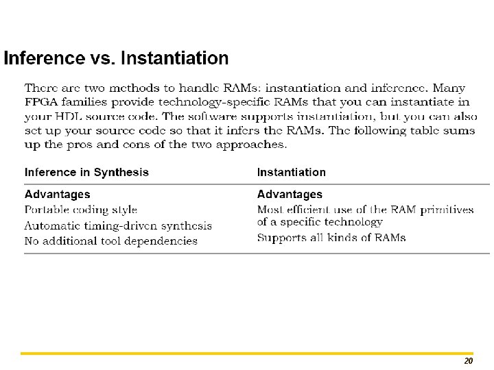
Inference vs. Instantiation 19

20

Generic Inferred ROM 21

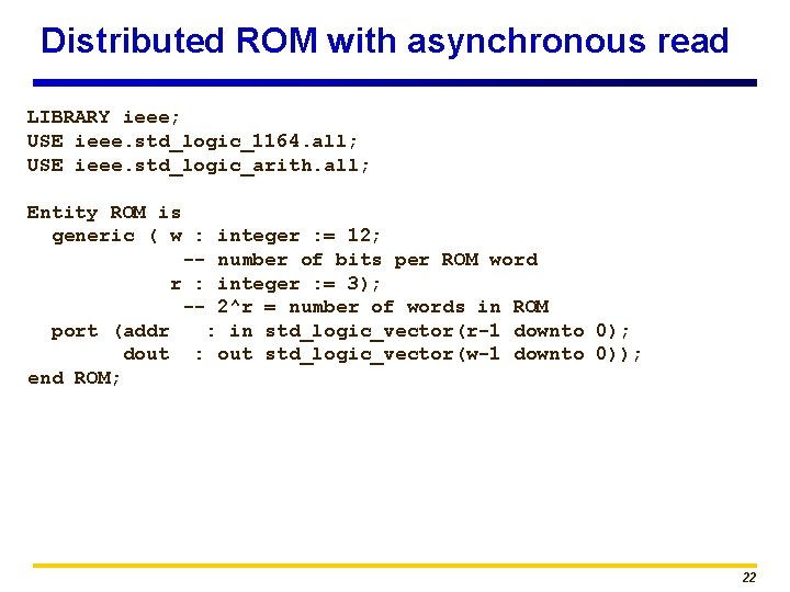
Distributed ROM with asynchronous read LIBRARY ieee; USE ieee. std_logic_1164. all; USE ieee. std_logic_arith. all; Entity ROM is generic ( w : integer : = 12; -- number of bits per ROM word r : integer : = 3); -- 2^r = number of words in ROM port (addr : in std_logic_vector(r-1 downto 0); dout : out std_logic_vector(w-1 downto 0)); end ROM; 22

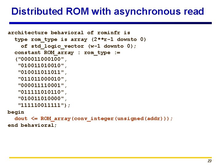
Distributed ROM with asynchronous read architecture behavioral of rominfr is type rom_type is array (2**r-1 downto 0) of std_logic_vector (w-1 downto 0); constant ROM_array : rom_type : = ("000011000100", "010011010010", "010011011011", "011011000010", "000011110001", "011111010110", "010011010000", "111110011111"); begin dout <= ROM_array(conv_integer(unsigned(addr))); end behavioral; 23

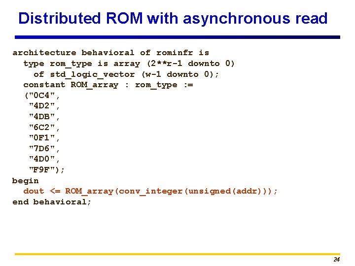
Distributed ROM with asynchronous read architecture behavioral of rominfr is type rom_type is array (2**r-1 downto 0) of std_logic_vector (w-1 downto 0); constant ROM_array : rom_type : = ("0 C 4", "4 D 2", "4 DB", "6 C 2", "0 F 1", "7 D 6", "4 D 0", "F 9 F"); begin dout <= ROM_array(conv_integer(unsigned(addr))); end behavioral; 24

Generic Inferred RAM 25

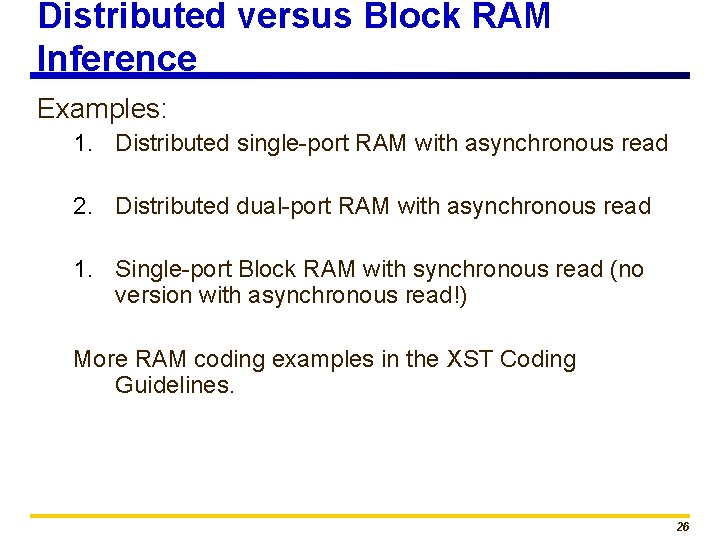
Distributed versus Block RAM Inference Examples: 1. Distributed single-port RAM with asynchronous read 2. Distributed dual-port RAM with asynchronous read 1. Single-port Block RAM with synchronous read (no version with asynchronous read!) More RAM coding examples in the XST Coding Guidelines. 26

Distributed RAM with asynchronous read 27

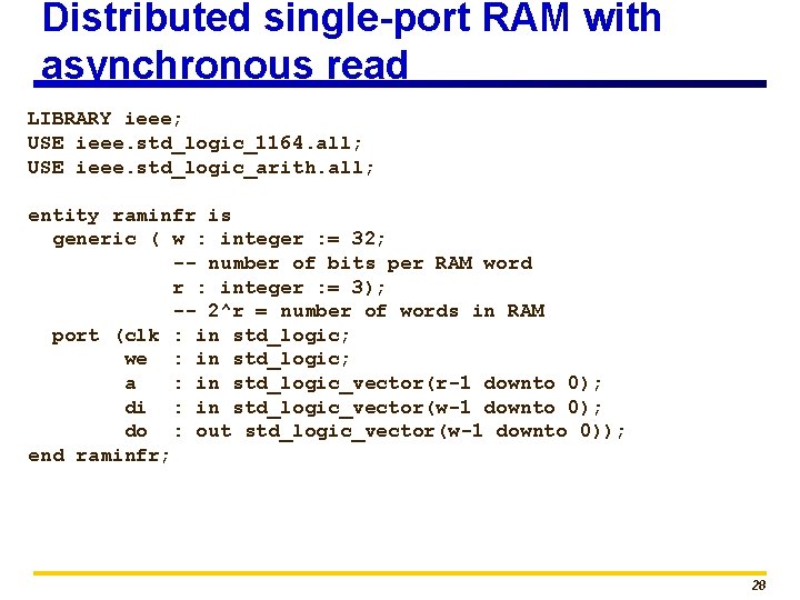
Distributed single-port RAM with asynchronous read LIBRARY ieee; USE ieee. std_logic_1164. all; USE ieee. std_logic_arith. all; entity raminfr is generic ( w : integer : = 32; -- number of bits per RAM word r : integer : = 3); -- 2^r = number of words in RAM port (clk : in std_logic; we : in std_logic; a : in std_logic_vector(r-1 downto 0); di : in std_logic_vector(w-1 downto 0); do : out std_logic_vector(w-1 downto 0)); end raminfr; 28

Distributed single-port RAM with asynchronous read architecture behavioral of raminfr is type ram_type is array (2**r-1 downto 0) of std_logic_vector (w-1 downto 0); signal RAM : ram_type; begin process (clk) begin if (clk'event and clk = '1') then if (we = '1') then RAM(conv_integer(unsigned(a))) <= di; end if; end process; do <= RAM(conv_integer(unsigned(a))); end behavioral; 29

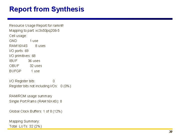
Report from Synthesis Resource Usage Report for raminfr Mapping to part: xc 3 s 50 pq 208 -5 Cell usage: GND 1 use RAM 16 X 4 S 8 uses I/O ports: 69 I/O primitives: 68 IBUF 36 uses OBUF 32 uses BUFGP 1 use I/O Register bits: 0 Register bits not including I/Os: 0 (0%) RAM/ROM usage summary Single Port Rams (RAM 16 X 4 S): 8 Global Clock Buffers: 1 of 8 (12%) Mapping Summary: Total LUTs: 32 (2%) 30

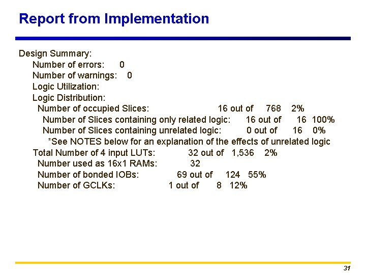
Report from Implementation Design Summary: Number of errors: 0 Number of warnings: 0 Logic Utilization: Logic Distribution: Number of occupied Slices: 16 out of 768 2% Number of Slices containing only related logic: 16 out of 16 100% Number of Slices containing unrelated logic: 0 out of 16 0% *See NOTES below for an explanation of the effects of unrelated logic Total Number of 4 input LUTs: 32 out of 1, 536 2% Number used as 16 x 1 RAMs: 32 Number of bonded IOBs: 69 out of 124 55% Number of GCLKs: 1 out of 8 12% 31

Distributed dual-port RAM with asynchronous read 32

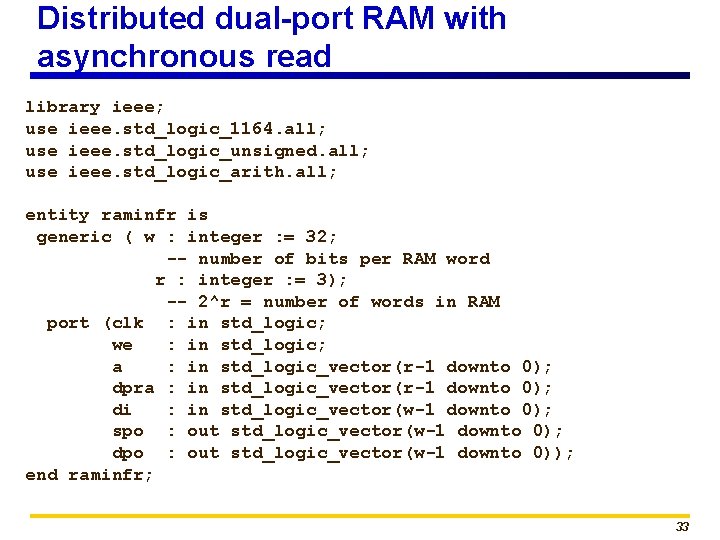
Distributed dual-port RAM with asynchronous read library ieee; use ieee. std_logic_1164. all; use ieee. std_logic_unsigned. all; use ieee. std_logic_arith. all; entity raminfr is generic ( w : integer : = 32; -- number of bits per RAM word r : integer : = 3); -- 2^r = number of words in RAM port (clk : in std_logic; we : in std_logic; a : in std_logic_vector(r-1 downto 0); dpra : in std_logic_vector(r-1 downto 0); di : in std_logic_vector(w-1 downto 0); spo : out std_logic_vector(w-1 downto 0); dpo : out std_logic_vector(w-1 downto 0)); end raminfr; 33

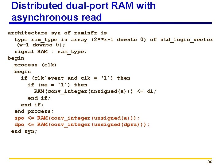
Distributed dual-port RAM with asynchronous read architecture syn of raminfr is type ram_type is array (2**r-1 downto 0) of std_logic_vector (w-1 downto 0); signal RAM : ram_type; begin process (clk) begin if (clk'event and clk = '1') then if (we = '1') then RAM(conv_integer(unsigned(a))) <= di; end if; end process; spo <= RAM(conv_integer(unsigned(a))); dpo <= RAM(conv_integer(unsigned(dpra))); end syn; 34

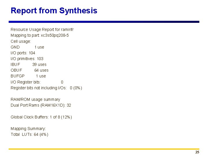
Report from Synthesis Resource Usage Report for raminfr Mapping to part: xc 3 s 50 pq 208 -5 Cell usage: GND 1 use I/O ports: 104 I/O primitives: 103 IBUF 39 uses OBUF 64 uses BUFGP 1 use I/O Register bits: 0 Register bits not including I/Os: 0 (0%) RAM/ROM usage summary Dual Port Rams (RAM 16 X 1 D): 32 Global Clock Buffers: 1 of 8 (12%) Mapping Summary: Total LUTs: 64 (4%) 35

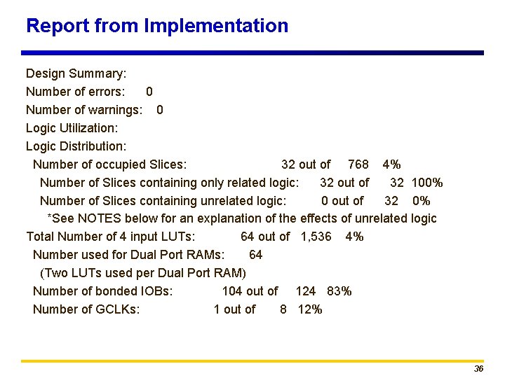
Report from Implementation Design Summary: Number of errors: 0 Number of warnings: 0 Logic Utilization: Logic Distribution: Number of occupied Slices: 32 out of 768 4% Number of Slices containing only related logic: 32 out of 32 100% Number of Slices containing unrelated logic: 0 out of 32 0% *See NOTES below for an explanation of the effects of unrelated logic Total Number of 4 input LUTs: 64 out of 1, 536 4% Number used for Dual Port RAMs: 64 (Two LUTs used per Dual Port RAM) Number of bonded IOBs: 104 out of 124 83% Number of GCLKs: 1 out of 8 12% 36

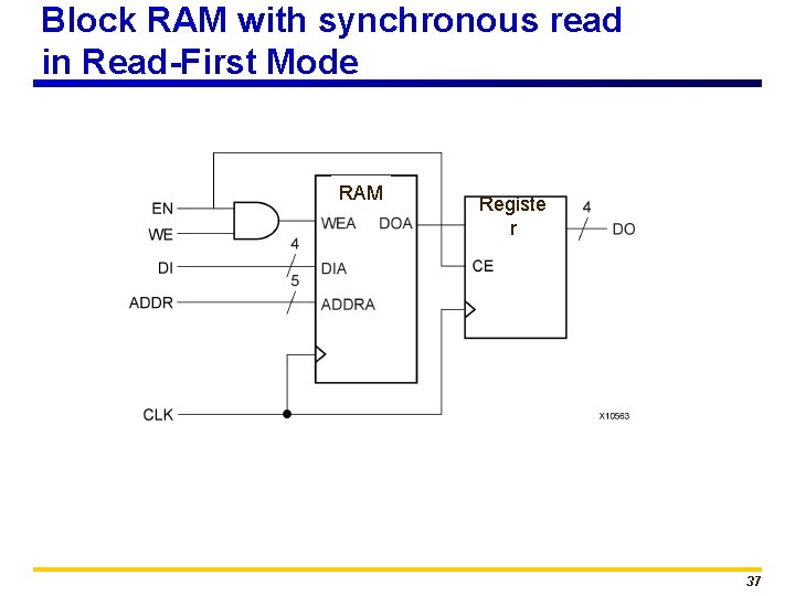
Block RAM with synchronous read in Read-First Mode RAM Registe r 37

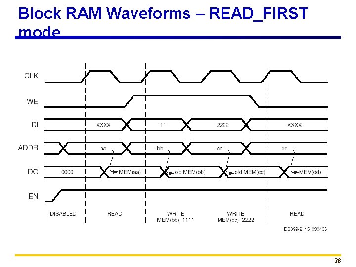
Block RAM Waveforms – READ_FIRST mode 38

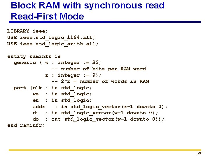
Block RAM with synchronous read Read-First Mode LIBRARY ieee; USE ieee. std_logic_1164. all; USE ieee. std_logic_arith. all; entity raminfr is generic ( w : integer : = 32; -- number of bits per RAM word r : integer : = 9); -- 2^r = number of words in RAM port (clk : in std_logic; we : in std_logic; en : in std_logic; addr : in std_logic_vector(r-1 downto 0); di : in std_logic_vector(w-1 downto 0); do : out std_logic_vector(w-1 downto 0)); end raminfr; 39

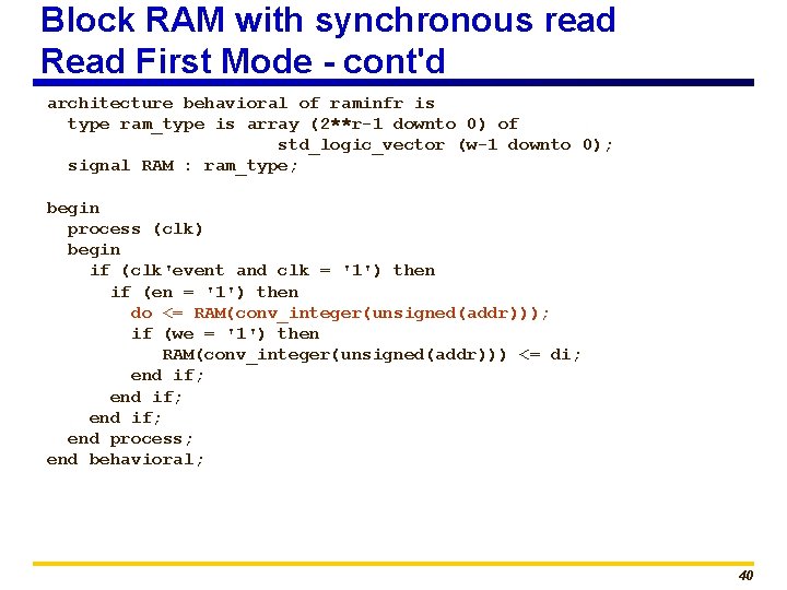
Block RAM with synchronous read Read First Mode - cont'd architecture behavioral of raminfr is type ram_type is array (2**r-1 downto 0) of std_logic_vector (w-1 downto 0); signal RAM : ram_type; begin process (clk) begin if (clk'event and clk = '1') then if (en = '1') then do <= RAM(conv_integer(unsigned(addr))); if (we = '1') then RAM(conv_integer(unsigned(addr))) <= di; end if; end process; end behavioral; 40

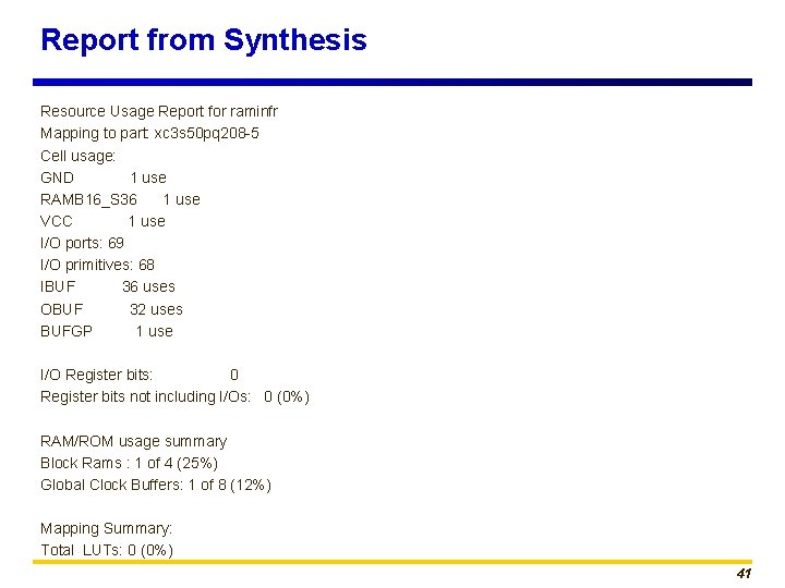
Report from Synthesis Resource Usage Report for raminfr Mapping to part: xc 3 s 50 pq 208 -5 Cell usage: GND 1 use RAMB 16_S 36 1 use VCC 1 use I/O ports: 69 I/O primitives: 68 IBUF 36 uses OBUF 32 uses BUFGP 1 use I/O Register bits: 0 Register bits not including I/Os: 0 (0%) RAM/ROM usage summary Block Rams : 1 of 4 (25%) Global Clock Buffers: 1 of 8 (12%) Mapping Summary: Total LUTs: 0 (0%) 41

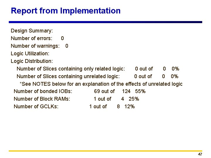
Report from Implementation Design Summary: Number of errors: 0 Number of warnings: 0 Logic Utilization: Logic Distribution: Number of Slices containing only related logic: 0 out of 0 0% Number of Slices containing unrelated logic: 0 out of 0 0% *See NOTES below for an explanation of the effects of unrelated logic Number of bonded IOBs: 69 out of 124 55% Number of Block RAMs: 1 out of 4 25% Number of GCLKs: 1 out of 8 12% 42

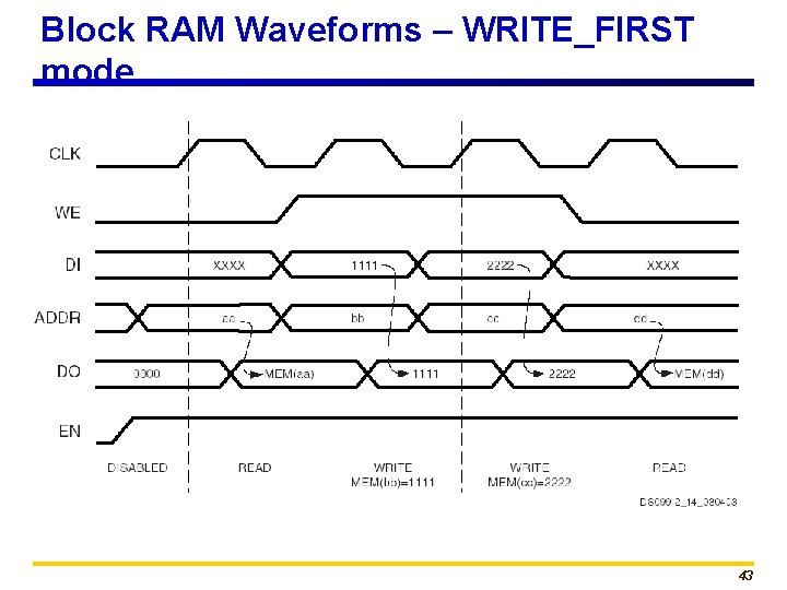
Block RAM Waveforms – WRITE_FIRST mode 43

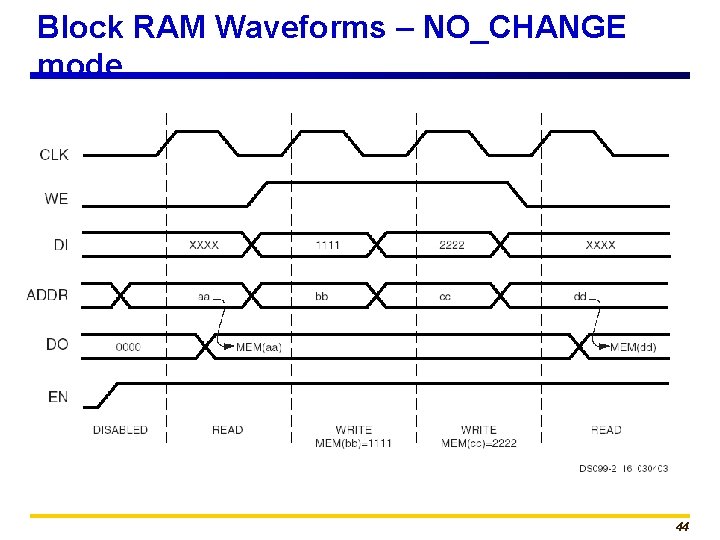
Block RAM Waveforms – NO_CHANGE mode 44

FPGA specific memories: Instantiation 45

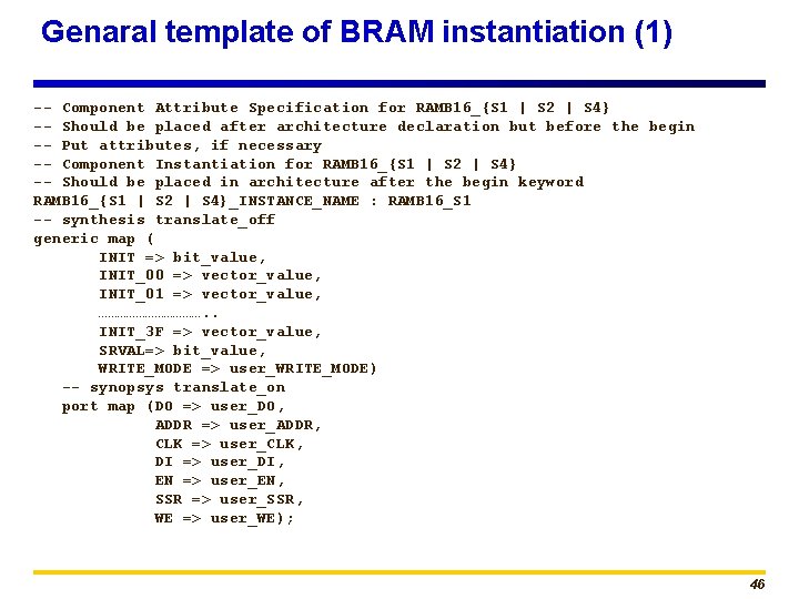
Genaral template of BRAM instantiation (1) -- Component Attribute Specification for RAMB 16_{S 1 | S 2 | S 4} -- Should be placed after architecture declaration but before the begin -- Put attributes, if necessary -- Component Instantiation for RAMB 16_{S 1 | S 2 | S 4} -- Should be placed in architecture after the begin keyword RAMB 16_{S 1 | S 2 | S 4}_INSTANCE_NAME : RAMB 16_S 1 -- synthesis translate_off generic map ( INIT => bit_value, INIT_00 => vector_value, INIT_01 => vector_value, ………………. . INIT_3 F => vector_value, SRVAL=> bit_value, WRITE_MODE => user_WRITE_MODE) -- synopsys translate_on port map (DO => user_DO, ADDR => user_ADDR, CLK => user_CLK, DI => user_DI, EN => user_EN, SSR => user_SSR, WE => user_WE); 46

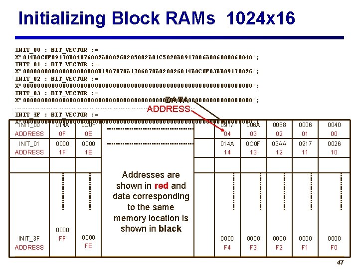
Initializing Block RAMs 1024 x 16 INIT_00 : BIT_VECTOR : = X"014 A 0 C 0 F 09170 A 04076802 A 800260205002 A 01 C 5020 A 0917006 A 006800060040"; INIT_01 : BIT_VECTOR : = X"0000000008000 A 1907070 A 1706070 A 020026014 A 0 C 0 F 03 AA 09170026"; INIT_02 : BIT_VECTOR : = X"00000000000000000000000000000000"; INIT_03 : BIT_VECTOR : = X"00000000000000000000000000000000"; DATA ………………………………………………………………… ADDRESS INIT_3 F : BIT_VECTOR : = X"00000000000000000000000000000000") INIT_00 014 A 0 C 0 F 0917 006 A ADDRESS 0 F 0 E 04 03 0068 02 0006 01 0040 00 INIT_01 ADDRESS 0000 1 F 0000 1 E INIT_3 F ADDRESS 0000 FF 0000 FE 014 A 14 0 C 0 F 13 03 AA 12 0917 11 0026 10 0000 F 4 0000 F 3 0000 F 2 0000 F 1 0000 F 0 Addresses are shown in red and data corresponding to the same memory location is shown in black 47

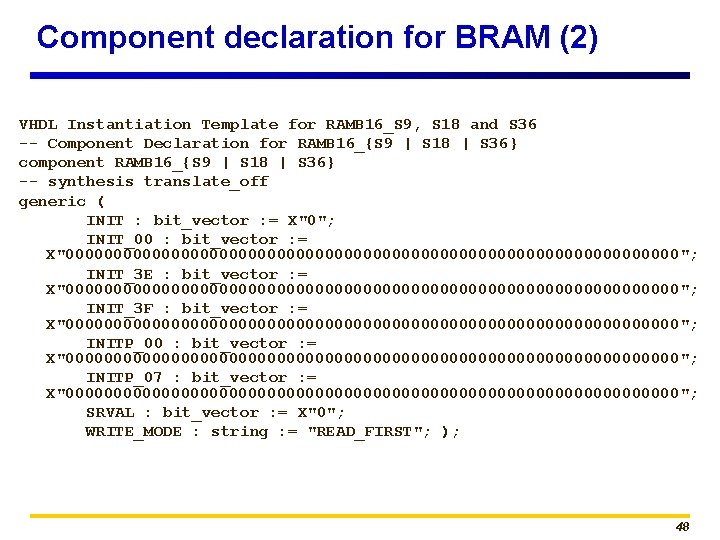
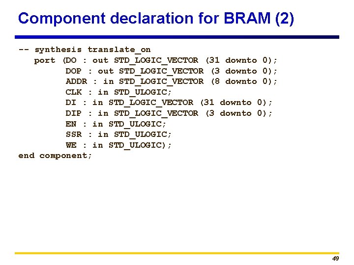
Component declaration for BRAM (2) VHDL Instantiation Template for RAMB 16_S 9, S 18 and S 36 -- Component Declaration for RAMB 16_{S 9 | S 18 | S 36} component RAMB 16_{S 9 | S 18 | S 36} -- synthesis translate_off generic ( INIT : bit_vector : = X"0"; INIT_00 : bit_vector : = X"00000000000000000000000000000000"; INIT_3 E : bit_vector : = X"00000000000000000000000000000000"; INIT_3 F : bit_vector : = X"00000000000000000000000000000000"; INITP_00 : bit_vector : = X"00000000000000000000000000000000"; INITP_07 : bit_vector : = X"00000000000000000000000000000000"; SRVAL : bit_vector : = X"0"; WRITE_MODE : string : = "READ_FIRST"; ); 48

Component declaration for BRAM (2) -- synthesis translate_on port (DO : out STD_LOGIC_VECTOR (31 downto 0); DOP : out STD_LOGIC_VECTOR (3 downto 0); ADDR : in STD_LOGIC_VECTOR (8 downto 0); CLK : in STD_ULOGIC; DI : in STD_LOGIC_VECTOR (31 downto 0); DIP : in STD_LOGIC_VECTOR (3 downto 0); EN : in STD_ULOGIC; SSR : in STD_ULOGIC; WE : in STD_ULOGIC); end component; 49

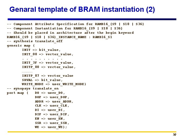
Genaral template of BRAM instantiation (2) -- Component Attribute Specification for RAMB 16_{S 9 | S 18 | S 36} -- Component Instantiation for RAMB 16_{S 9 | S 18 | S 36} -- Should be placed in architecture after the begin keyword RAMB 16_{S 9 | S 18 | S 36}_INSTANCE_NAME : RAMB 16_S 1 -- synthesis translate_off generic map ( INIT => bit_value, INIT_00 => vector_value, . . INIT_3 F => vector_value, INITP_00 => vector_value, …………… INITP_07 => vector_value SRVAL => bit_value, WRITE_MODE => user_WRITE_MODE) -- synopsys translate_on port map ( DO => user_DO, DOP => user_DOP, ADDR => user_ADDR, CLK => user_CLK, DI => user_DI, DIP => user_DIP, EN => user_EN, SSR => user_SSR, WE => user_WE); 50

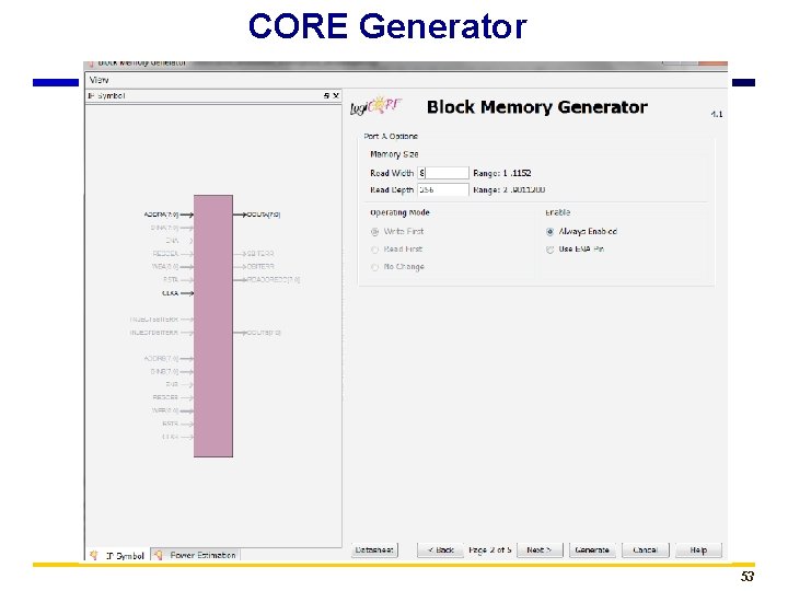
Using CORE Generator 51

CORE Generator 52

CORE Generator 53