FPGA for Dummies Modern FPGA architecture ESS FPGA



- Slides: 32

FPGA for Dummies Modern FPGA architecture ESS | FPGA for Dummies | 2016 -08 -30| Maurizio Donna

FPGA for Dummies • FPGA Architecture: Ø basic blocks (Logic, FFs, wires and IOs); Ø additional modern elements; • FPGA Programming: ØHDL languages; ØDesign flow; • FPGA DSP: ØArithmetic, FFT and filters; ESS | FPGA for Dummies | 2015 -12 -08 | Maurizio Donna

FPGA for Dummies • FPGA Architecture: Ø basic blocks (Logic, FFs, wires and IOs); Ø additional modern elements; • FPGA Programming: ØHDL languages; ØDesign flow; • FPGA DSP: ØArithmetic, FFT and filters; ESS | FPGA for Dummies | 2015 -12 -08 | Maurizio Donna

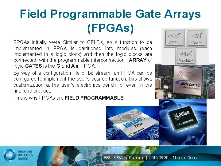
Field Programmable Gate Arrays (FPGAs) FPGAs initially were Similar to CPLDs, so a function to be implemented in FPGA is partitioned into modules (each implemented in a logic block) and then the logic blocks are connected with the programmable interconnection: ARRAY of logic GATES is the G and A in FPGA. By way of a configuration file or bit stream, an FPGA can be configured to implement the user’s desired function: this allows customization at the user’s electronics bench, or even in the final end product. This is why FPGAs are FIELD PROGRAMMABLE. ESS | FPGA for Dummies | 2016 -08 -30| Maurizio Donna

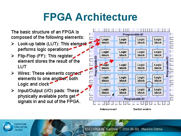
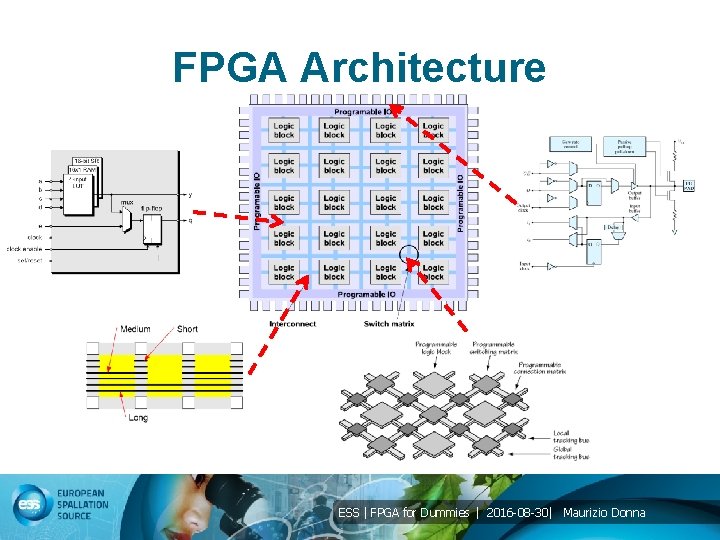
FPGA Architecture The basic structure of an FPGA is composed of the following elements: Ø Look-up table (LUT): This element performs logic operations Ø Flip-Flop (FF): This register element stores the result of the LUT Ø Wires: These elements connect elements to one another, both Logic and clock Ø Input/Output (I/O) pads: These physically available ports get signals in and out of the FPGA. ESS | FPGA for Dummies | 2016 -08 -30| Maurizio Donna

FPGA Architecture ESS | FPGA for Dummies | 2016 -08 -30| Maurizio Donna

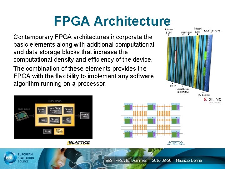
FPGA Architecture Contemporary FPGA architectures incorporate the basic elements along with additional computational and data storage blocks that increase the computational density and efficiency of the device. The combination of these elements provides the FPGA with the flexibility to implement any software algorithm running on a processor. ESS | FPGA for Dummies | 2016 -08 -30| Maurizio Donna

FPGA Architecture These additional elements, which are discussed in the following sections, are: Ø Embedded memories for distributed data storage; Ø Phase-locked loops (PLLs) for driving the FPGA fabric at different clock rates; Ø High-speed serial transceivers; Ø Off-chip memory controllers; Ø Multiply-accumulate blocks; Ø Embedded processors. ESS | FPGA for Dummies | 2016 -08 -30| Maurizio Donna

FPGA Architecture These additional elements, which are discussed in the following sections, are: Ø Embedded memories for distributed data storage; Ø Phase-locked loops (PLLs) for driving the FPGA fabric at different clock rates; Ø High-speed serial transceivers; Ø Off-chip memory controllers; Ø Multiply-accumulate blocks; Ø Embedded processors. ESS | FPGA for Dummies | 2016 -08 -30| Maurizio Donna

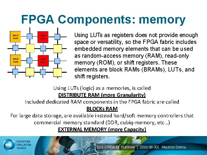
FPGA Components: memory Block RAM Logic block Using LUTs as registers does not provide enough space or versatility, so the FPGA fabric includes embedded memory elements that can be used as random-access memory (RAM), read-only memory (ROM), or shift registers. These elements are block RAMs (BRAMs), LUTs, and shift registers. Using LUTs (logic) as a memories, is called DISTRIBUTE RAM (more Granularity) Included dedicated RAM components in the FPGA fabric are called BLOCKs RAM For large data storage, are available instead hard/soft memory controllers that commercial memory standard (DDR, cubiq-memory, etc…) EXTERNAL MEMORY (more Capacity) ESS | FPGA for Dummies | 2016 -08 -30| Maurizio Donna

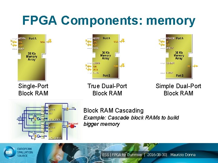
FPGA Components: memory Single-Port Block RAM True Dual-Port Block RAM Simple Dual-Port Block RAM Cascading Example: Cascade block RAMs to build bigger memory ESS | FPGA for Dummies | 2016 -08 -30| Maurizio Donna

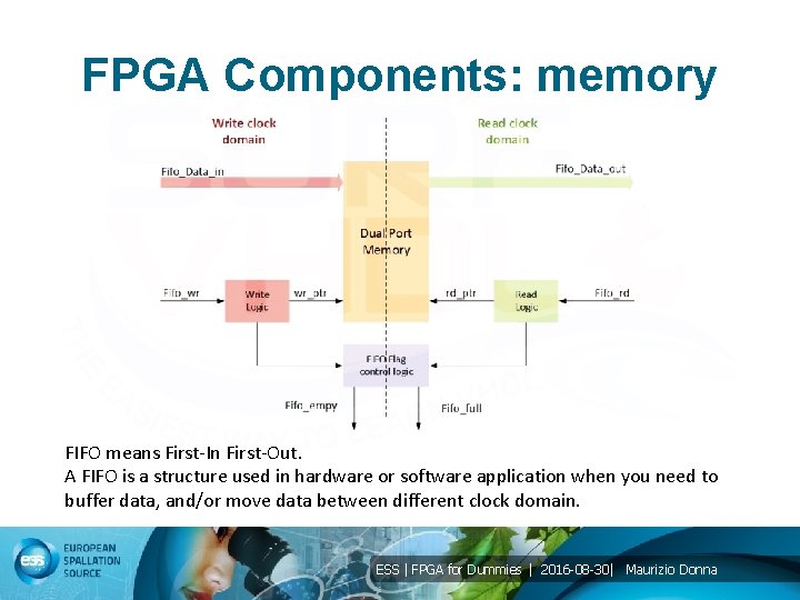
FPGA Components: memory FIFO means First-In First-Out. A FIFO is a structure used in hardware or software application when you need to buffer data, and/or move data between different clock domain. ESS | FPGA for Dummies | 2016 -08 -30| Maurizio Donna

FPGA Architecture These additional elements, which are discussed in the following sections, are: Ø Embedded memories for distributed data storage; Ø Phase-locked loops (PLLs) for driving the FPGA fabric at different clock rates; Ø High-speed serial transceivers; Ø Off-chip memory controllers; Ø Multiply-accumulate blocks; Ø Embedded processors. ESS | FPGA for Dummies | 2016 -08 -30| Maurizio Donna

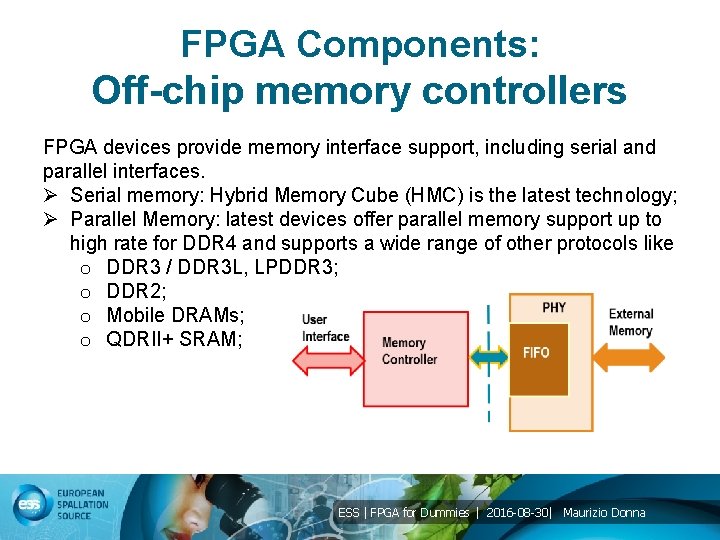
FPGA Components: Off-chip memory controllers FPGA devices provide memory interface support, including serial and parallel interfaces. Ø Serial memory: Hybrid Memory Cube (HMC) is the latest technology; Ø Parallel Memory: latest devices offer parallel memory support up to high rate for DDR 4 and supports a wide range of other protocols like o DDR 3 / DDR 3 L, LPDDR 3; o DDR 2; o Mobile DRAMs; o QDRII+ SRAM; ESS | FPGA for Dummies | 2016 -08 -30| Maurizio Donna

FPGA Architecture These additional elements, which are discussed in the following sections, are: Ø Embedded memories for distributed data storage; Ø Phase-locked loops (PLLs) for driving the FPGA fabric at different clock rates; Ø High-speed serial transceivers; Ø Off-chip memory controllers; Ø Multiply-accumulate blocks; Ø Embedded processors. ESS | FPGA for Dummies | 2016 -08 -30| Maurizio Donna

FPGA Components: clocking All synchronous designs need at least one external clock reference, many designs require several clock sources!!! In FPGA there are several layers of metallization to interconnect the Logic, and there are special one to distribute the clocks to all the Flip Flops (FF). Modern applications have complex clocking requirements: Ø Extremely high-performance clock signals; Ø Support for multiple frequency domains across a wide frequency range; Ø De-skewing of clocks relative to one another; Ø Low jitter and precise duty cycle to maintain the widest possible data valid window; Ø Lowest possible system power ESS | FPGA for Dummies | 2016 -08 -30| Maurizio Donna

FPGA Components: clocking A Phase Lock Loop (PLL) is a control system that uses a Controlled Voltage Oscillator (VCO) to generates an output signal whose phase is related to the phase of an input signal; A Delay-Locked Loop (DLL) is similar to a PLL but instead of the VCO to vary the frequency, introduce fixed delay to change the phase; Both components could replicate and/or generate new clocks combination, according to the input clock frequency. PLL are more “clear” than DLL, but DLL are easier to integrate in logic than PLL. ESS | FPGA for Dummies | 2016 -08 -30| Maurizio Donna

FPGA Architecture These additional elements, which are discussed in the following sections, are: Ø Embedded memories for distributed data storage; Ø Phase-locked loops (PLLs) for driving the FPGA fabric at different clock rates; Ø High-speed serial transceivers; Ø Off-chip memory controllers; Ø Multiply-accumulate blocks; Ø Embedded processors. ESS | FPGA for Dummies | 2016 -08 -30| Maurizio Donna

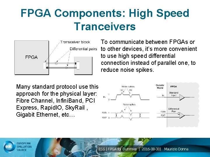
FPGA Components: High Speed Tranceivers To communicate between FPGAs or to other devices, it’s more convenient to use high speed differential connection instead of parallel one, to reduce noise spikes. Many standard protocol use this approach for the physical layer: Fibre Channel, Infini. Band, PCI Express, Rapid. IO, Sky. Rail , Gigabit Ethernet, etc… ESS | FPGA for Dummies | 2016 -08 -30| Maurizio Donna

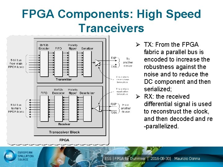
FPGA Components: High Speed Tranceivers Ø TX: From the FPGA fabric a parallel bus is encoded to increase the robustness against the noise and to reduce the DC component and then serialized; Ø RX: the received differential signal is used to reconstruct the clock, and then decoded and re -parallelized. ESS | FPGA for Dummies | 2016 -08 -30| Maurizio Donna

FPGA Architecture These additional elements, which are discussed in the following sections, are: Ø Embedded memories for distributed data storage; Ø Phase-locked loops (PLLs) for driving the FPGA fabric at different clock rates; Ø High-speed serial transceivers; Ø Off-chip memory controllers; Ø Multiply-accumulate blocks; Ø Embedded processors. ESS | FPGA for Dummies | 2016 -08 -30| Maurizio Donna

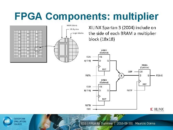
FPGA Components: multiplier XILINX Spartan 3 (2004) include on the side of each BRAM a multiplier block (18 x 18) ESS | FPGA for Dummies | 2016 -08 -30| Maurizio Donna

FPGA Components: multiplier Altera Cyclone II (2005) has one to three columns of embedded multipliers; each embedded multiplier can be configured to support : Ø One 18 x 18 multiplier Ø Two 9 x 9 multipliers ESS | FPGA for Dummies | 2016 -08 -30| Maurizio Donna

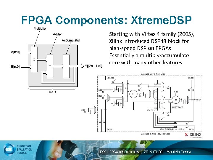
FPGA Components: Xtreme. DSP Starting with Virtex 4 family (2005), Xilinx introduced DSP 48 block for high-speed DSP on FPGAs Essentially a multiply-accumulate core with many other features ESS | FPGA for Dummies | 2016 -08 -30| Maurizio Donna

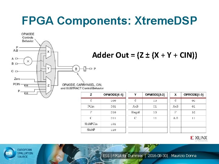
FPGA Components: Xtreme. DSP Adder Out = (Z ± (X + Y + CIN)) ESS | FPGA for Dummies | 2016 -08 -30| Maurizio Donna

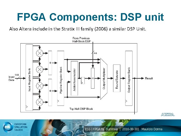
FPGA Components: DSP unit Also Altera include in the Stratix III family (2006) a similar DSP Unit. ESS | FPGA for Dummies | 2016 -08 -30| Maurizio Donna

FPGA Architecture These additional elements, which are discussed in the following sections, are: Ø Embedded memories for distributed data storage; Ø Phase-locked loops (PLLs) for driving the FPGA fabric at different clock rates; Ø High-speed serial transceivers; Ø Off-chip memory controllers; Ø Multiply-accumulate blocks; Ø Embedded processors. ESS | FPGA for Dummies | 2016 -08 -30| Maurizio Donna

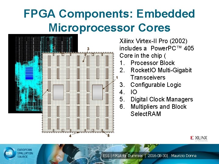
FPGA Components: Embedded Microprocessor Cores Xilinx Virtex-II Pro (2002) includes a Power. PC™ 405 Core in the chip ( 1. Processor Block 2. Rocket. IO Multi-Gigabit Transceivers 3. Configurable Logic 4. IO 5. Digital Clock Managers 6. Multipliers and Block Select. RAM ESS | FPGA for Dummies | 2016 -08 -30| Maurizio Donna

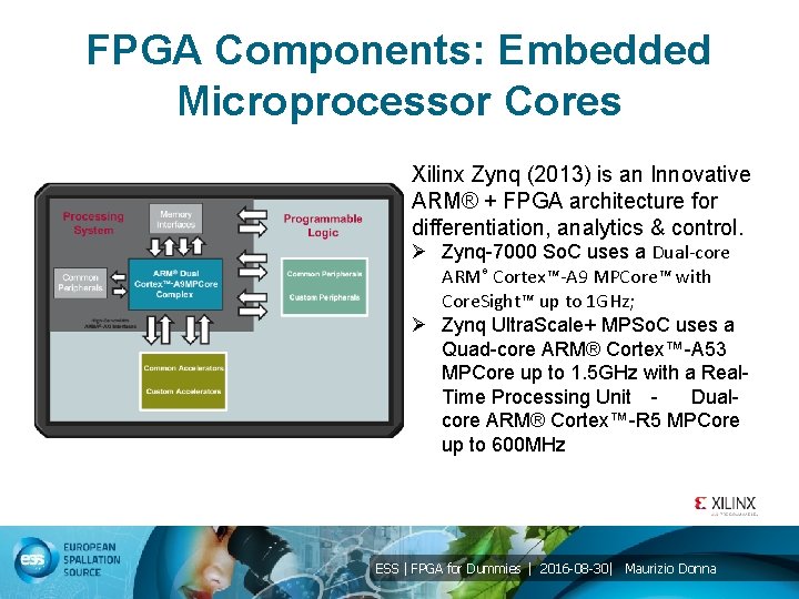
FPGA Components: Embedded Microprocessor Cores Xilinx Zynq (2013) is an Innovative ARM® + FPGA architecture for differentiation, analytics & control. Ø Zynq-7000 So. C uses a Dual-core ARM® Cortex™-A 9 MPCore™ with Core. Sight™ up to 1 GHz; Ø Zynq Ultra. Scale+ MPSo. C uses a Quad-core ARM® Cortex™-A 53 MPCore up to 1. 5 GHz with a Real. Time Processing Unit Dualcore ARM® Cortex™-R 5 MPCore up to 600 MHz ESS | FPGA for Dummies | 2016 -08 -30| Maurizio Donna

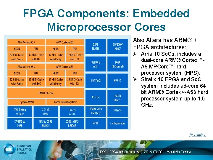
FPGA Components: Embedded Microprocessor Cores Also Altera has ARM® + FPGA architectures: Ø Arria 10 So. Cs, includes a dual-core ARM® Cortex™A 9 MPCore™ hard processor system (HPS); Ø Stratix 10 FPGA and So. C system includes ad-core 64 bit ARM® Cortex®-A 53 hard processor system up to 1. 5 GHz; ESS | FPGA for Dummies | 2016 -08 -30| Maurizio Donna

Questions ESS | FPGA for Dummies | 2016 -08 -30| Maurizio Donna

ESS | FPGA for Dummies | 2016 -08 -30| Maurizio Donna