Configuration Memory Frames Example of the Virtex 5
- Slides: 15

Configuration Memory Frames Example of the Virtex 5 LX 30 ff 324 Phd student: BELAID Ikbel belaidikbel@yahoo. fr Supervisor: Fabrice MULLER fabrice. muller@unice. fr University of Nice Sophia Antipolis / CNRS 7 March 2008

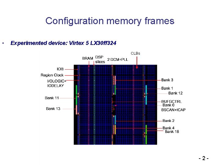
Configuration memory frames • Experimented device: Virtex 5 LX 30 ff 324 CLBs - 2 -

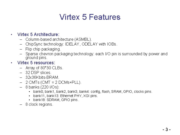
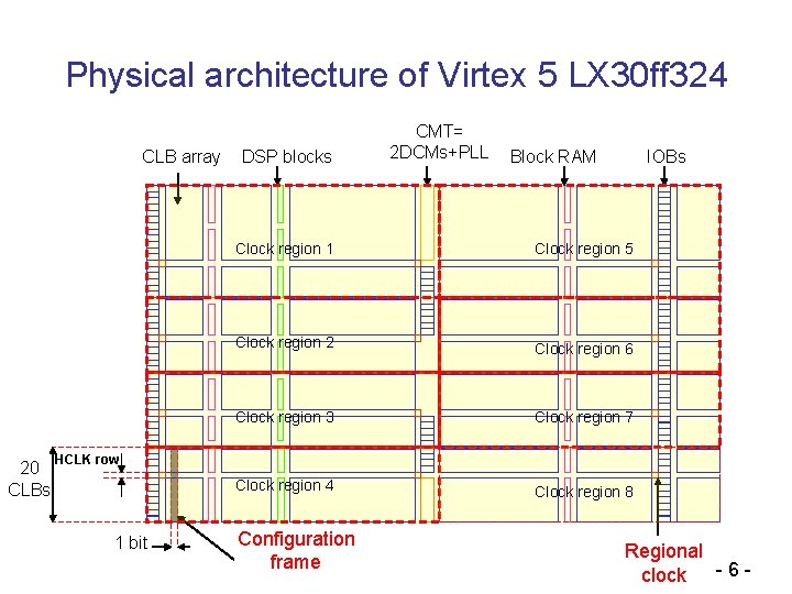
Virtex 5 Features • Virtex 5 Architecture: – – • Column-based architecture (ASMBL). Chip. Sync technology: IDELAY, ODELAY with IOBs. Flip chip packaging. Sparse chevron packaging technology: each I/O pin is surrounded by power and ground pins. Virtex 5 resources: – – – Array of 80*30 CLBs. 32 DSP slices. 32 x 36 Kbits-BRAM. 2 CMTs (CMT = 2 DCMs+PLL). 8 banks (220 I/Os): • bank 0, bank 1, bank 2, bank 3, bank 4: config, flash, SRAM, GPIO, clocks pins. • bank 11, bank 13: Ethernet PHY, XGI pins. • bank 18: SDRAM, GPIO pins. – 8 clock regions. - 3 -

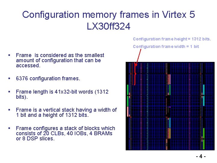
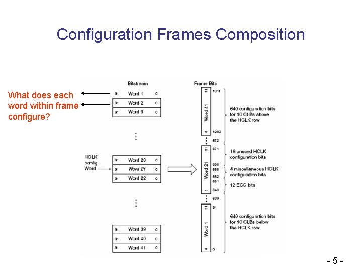
Configuration memory frames in Virtex 5 LX 30 ff 324 Configuration frame height = 1312 bits. Configuration frame width = 1 bit § Frame is considered as the smallest amount of configuration that can be accessed. § 6376 configuration frames. § Frame length is 41 x 32 -bit words (1312 bits). § Frame is a vertical stack having a width of 1 bit and a height of 1312 bits. § Frame configures a stack of blocks which consists of 20 CLBs, 40 IOBs, 4 BRAMs or 8 DSP slices. - 4 -

Configuration Frames Composition What does each word within frame configure? - 5 -

Physical architecture of Virtex 5 LX 30 ff 324 CLB array 20 CLBs DSP blocks CMT= 2 DCMs+PLL Block RAM IOBs Clock region 1 Clock region 5 Clock region 2 Clock region 6 Clock region 3 Clock region 7 Clock region 4 Clock region 8 HCLK row 1 bit Configuration frame Regional clock - 6 -

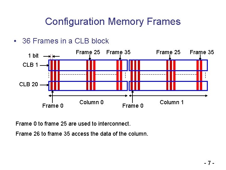
Configuration Memory Frames • 36 Frames in a CLB block Frame 25 1 bit Frame 35 Frame 25 Frame 35 CLB 1 CLB 20 Frame 0 Column 1 Frame 0 to frame 25 are used to interconnect. Frame 26 to frame 35 access the data of the column. - 7 -

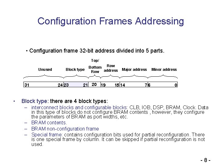
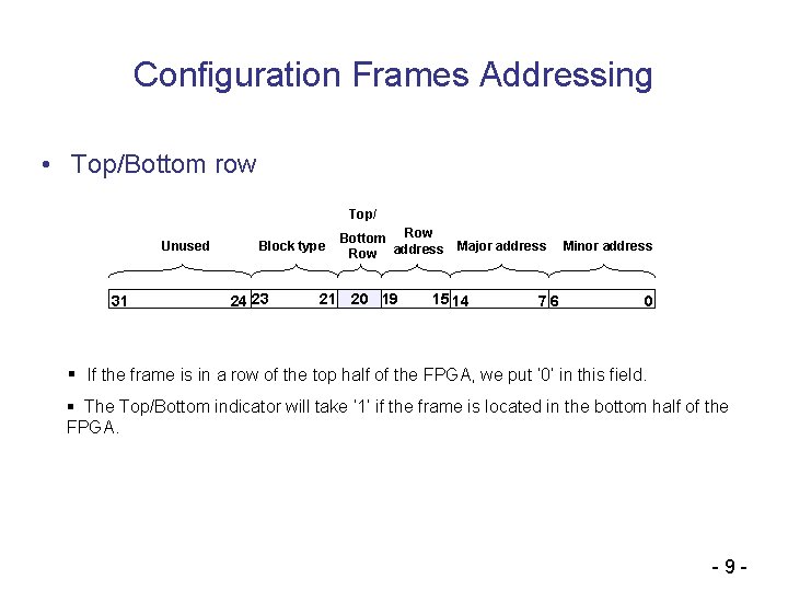
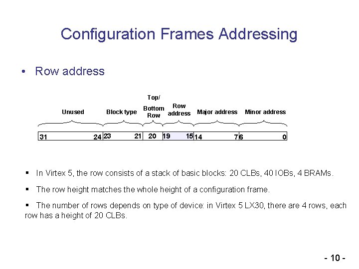
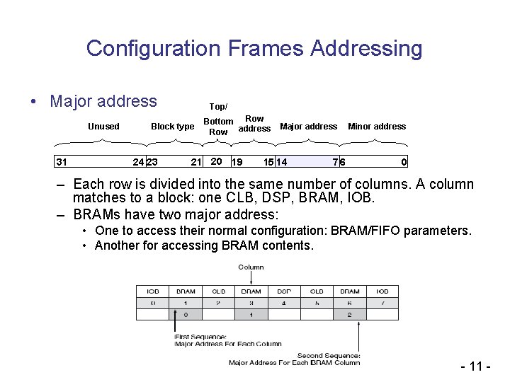
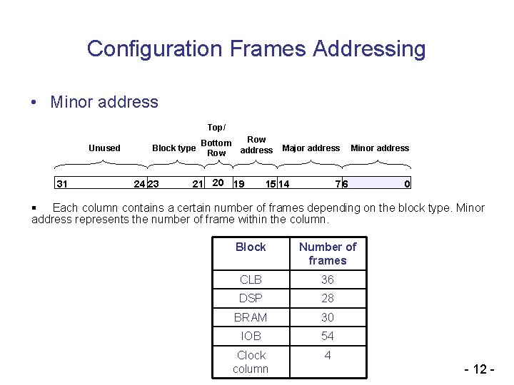
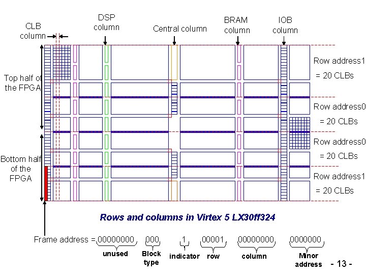
Configuration Frames Addressing • Configuration frame 32 -bit address divided into 5 parts. Top/ Unused 31 • Block type 24 23 21 Bottom Row address Major address 20 19 15 14 Minor address 7 6 0 Block type: there are 4 block types: – interconnect blocks and configurable blocks: CLB, IOB, DSP, BRAM, Clock. Data in this type of blocks do not configure BRAM contents , however, they configure the parameters of BRAM as port widths, etc. – BRAM contents. – BRAM non-configuration frame – Special frame: contains configuration bits used for partial reconfiguration. There is one special frame by column. It can be skipped if partial reconfiguration is not used. - 8 -

Configuration Frames Addressing • Top/Bottom row Top/ Unused 31 Block type 24 23 Bottom Row address 21 20 19 Major address Minor address 15 14 7 6 0 § If the frame is in a row of the top half of the FPGA, we put ‘ 0’ in this field. § The Top/Bottom indicator will take ‘ 1’ if the frame is located in the bottom half of the FPGA. - 9 -

Configuration Frames Addressing • Row address Top/ Unused 31 Block type 24 23 Bottom Row address 21 20 19 Major address Minor address 15 14 7 6 0 § In Virtex 5, the row consists of a stack of basic blocks: 20 CLBs, 40 IOBs, 4 BRAMs. § The row height matches the whole height of a configuration frame. § The number of rows depends on type of device: in Virtex 5 LX 30, there are 4 rows, each row has a height of 20 CLBs. - 10 -

Configuration Frames Addressing • Major address Unused 31 Block type 24 23 21 Top/ Bottom Row address Major address 20 19 15 14 Minor address 7 6 0 – Each row is divided into the same number of columns. A column matches to a block: one CLB, DSP, BRAM, IOB. – BRAMs have two major address: • One to access their normal configuration: BRAM/FIFO parameters. • Another for accessing BRAM contents. - 11 -

Configuration Frames Addressing • Minor address Top/ Unused 31 Block type Bottom Row 24 23 21 Row address Major address 20 19 15 14 Minor address 7 6 0 § Each column contains a certain number of frames depending on the block type. Minor address represents the number of frame within the column. Block Number of frames CLB 36 DSP 28 BRAM 30 IOB 54 Clock column 4 - 12 -

CLB column DSP column Central column BRAM column IOB column Row address 1 = 20 CLBs Top half of the FPGA Row address 0 = 20 CLBs Bottom half of the FPGA Row address 1 = 20 CLBs Rows and columns in Virtex 5 LX 30 ff 324 Frame address = 0000 000 1 00001 0000000 unused Block type indicator row column Minor address - 13 -

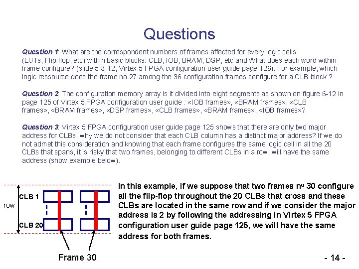
Questions Question 1: What are the correspondent numbers of frames affected for every logic cells (LUTs, Flip-flop, etc) within basic blocks: CLB, IOB, BRAM, DSP, etc and What does each word within frame configure? (slide 5 & 12, Virtex 5 FPGA configuration user guide page 126). For example, which logic ressource does the frame no 27 among the 36 configuration frames configure for a CLB block ? Question 2: The configuration memory array is it divided into eight segments as shown on figure 6 -12 in page 125 of Virtex 5 FPGA configuration user guide : «IOB frames» , «BRAM frames» , «CLB frames» , «BRAM frames» , «DSP frames» , «CLB frames» , «BRAM frames» , «IOB frames» ? Question 3: Virtex 5 FPGA configuration user guide page 125 shows that there are only two major address for CLBs, why we do not consider that each CLB column has a distinct major address? If we do not admet this consideration and knowing that each frame configures the same logic cell in all the 20 CLBs that spans, it is risky that two frames, belonging to different CLBs in a row, will have the same address (show example below). In this example, if we suppose that two frames no 30 configure all the flip-flop throughout the 20 CLBs that cross and these CLBs are located in the same row and if we consider the major address is 2 by following the addressing in Virtex 5 FPGA configuration user guide page 125, we will have the same address for both frames. CLB 1 row CLB 20 Frame 30 - 14 -

Questions Question 4: what is the interest of using the frame having as block type « BRAM non configuration frame » and what does it configure in the BRAM blocks? (referencing to Virtex 5 FPGA configuration user guide page 125) Question 5: How we use special frame to perform partial reconfiguration: its addressing and its data? (referencing to Virtex 5 FPGA configuration user guide page 125) Question 6: Possibility of writing only 1024 x 32 -bit words sequentially in FDRI register with automaticaly addressing of configuration frames? After 1024 x 32 -bit words, we must define the next frame address in FDRI? (referencing to Virtex 5 FPGA configuration user guide page 121) Question 7: Is it advantegous, and not restricted, to allocate reconfigurable region of 20 CLBs height (or multiply of 20 CLBs) and having a width ranging from one CLB to a whole device width? In fact a module of 20 -CLB height is beneficial at level of reconfiguration by minimizing the overhead of frames to reconfigure (decreasing the number of frames to reconfigure) and ensures power enhancement and performance improvement, etc. Can you confirm that? Question 8: How we can spot blocks of interconnect in Planahead? - 15 -