Redefining the FPGA Virtex as a System Component

- Slides: 16

Redefining the FPGA

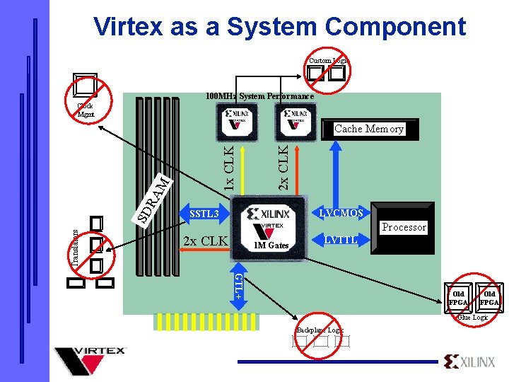
Virtex as a System Component Custom Logic 100 MHz System Performance Clock Mgmt Translators SD RA 2 x CLK M 1 x CLK Cache Memory LVCMOS SSTL 3 Processor 2 x CLK 1 M Gates LVTTL GTL+ Old FPGA Glue Logic Backplane Logic

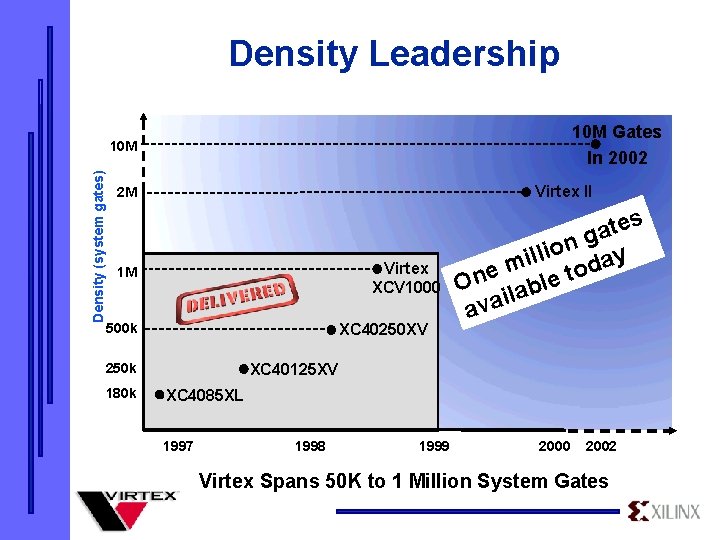
Density Leadership 10 M Gates In 2002 Density (system gates) 10 M Virtex II 2 M Virtex XCV 1000 1 M 500 k XC 40250 XV XC 40125 XV 250 k 180 k es t a g n o i y ill a m d o One lable t i ava XC 4085 XL 1997 1998 1999 2000 2002 Virtex Spans 50 K to 1 Million System Gates

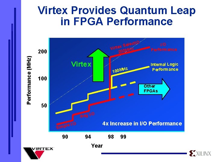
Virtex Provides Quantum Leap in FPGA Performance (MHz) 200 Virtex lect. IO e S x Virte MHz 200 I/O Performance Hz Internal Logic Performance 100 M 100 Other FPGAs 50 /O Reg I 4 x Increase in I/O Performance le I/O Simp 90 94 Year 98 99

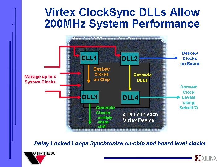
Virtex Clock. Sync DLLs Allow 200 MHz System Performance DLL 1 Manage up to 4 System Clocks Deskew Clocks on Chip DLL 3 Generate Clocks -multiply -divide -shift DLL 2 Deskew Clocks on Board Cascade DLLs DLL 4 Convert Clock Levels using Select. I/O 4 DLLs in each Virtex Device Delay Locked Loops Synchronize on-chip and board level clocks

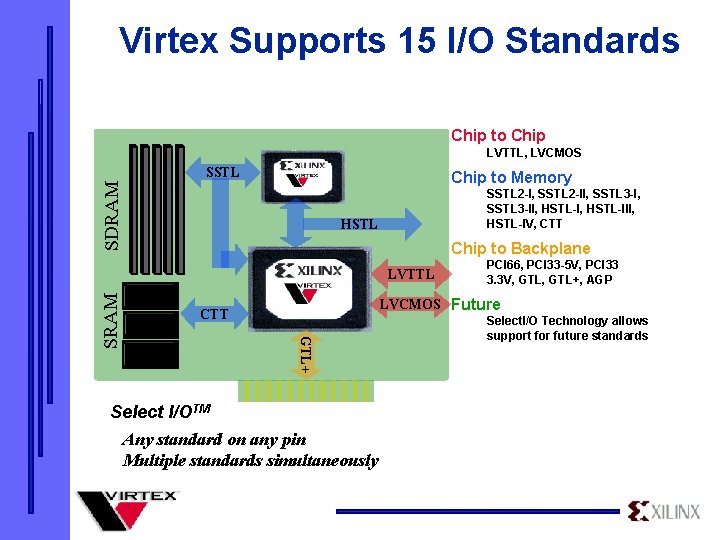
Virtex Supports 15 I/O Standards Chip to Chip SDRAM LVTTL, LVCMOS SSTL Chip to Memory SSTL 2 -I, SSTL 2 -II, SSTL 3 -II, HSTL-III, HSTL-IV, CTT HSTL Chip to Backplane PCI 66, PCI 33 -5 V, PCI 33 3. 3 V, GTL+, AGP LVCMOS Future CTT GTL+ SRAM LVTTL Select I/OTM Any standard on any pin Multiple standards simultaneously Select. I/O Technology allows support for future standards

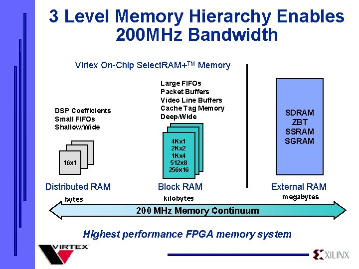
3 Level Memory Hierarchy Enables 200 MHz Bandwidth Virtex On-Chip Select. RAM+TM Memory DSP Coefficients Small FIFOs Shallow/Wide 4 Kx 1 2 Kx 2 1 Kx 4 512 x 8 256 x 16 16 x 1 Distributed RAM bytes Large FIFOs Packet Buffers Video Line Buffers Cache Tag Memory Deep/Wide SDRAM ZBT SSRAM SGRAM Block RAM External RAM kilobytes megabytes 200 MHz Memory Continuum Highest performance FPGA memory system

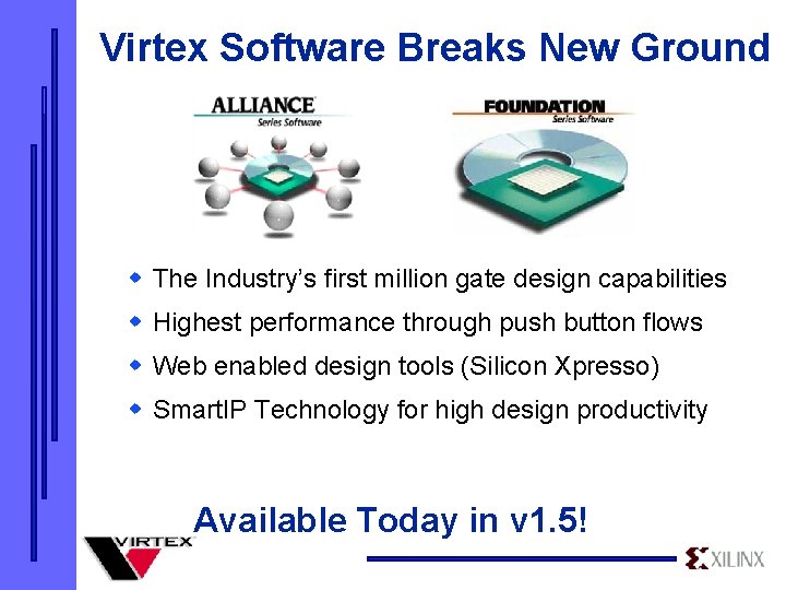
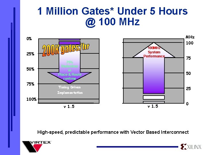
Virtex Software Breaks New Ground w The Industry’s first million gate design capabilities w Highest performance through push button flows w Web enabled design tools (Silicon Xpresso) w Smart. IP Technology for high design productivity Available Today in v 1. 5!

1 Million Gates* Under 5 Hours @ 100 MHz 100 0% 100 MHz System Performance 25% 50% 75% Reduction in Place & Route runtime 50 Timing Driven 25 Implementation 100% v 1. 5 75 v 1. 5 0 High-speed, predictable performance with Vector Based Interconnect

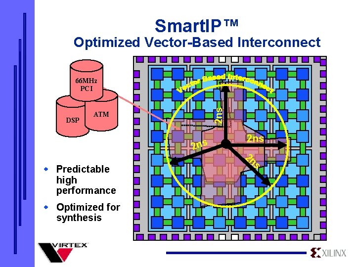
Smart. IP™ Optimized Vector-Based Interconnect DSP 2 ns 66 MHz PCI ATM 2 ns s w Optimized for synthesis 2 n w Predictable high performance 2 ns

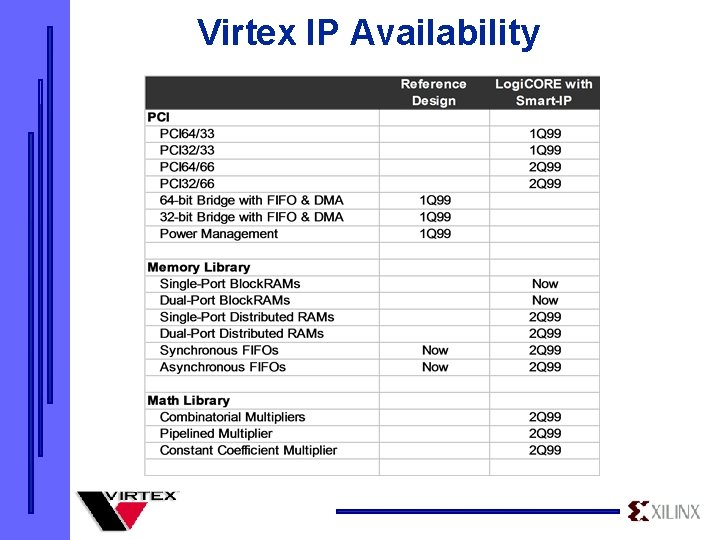
Virtex IP Availability

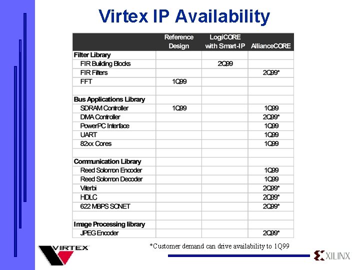
Virtex IP Availability *Customer demand can drive availability to 1 Q 99

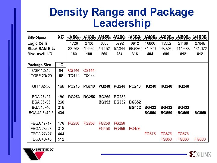
Density Range and Package Leadership

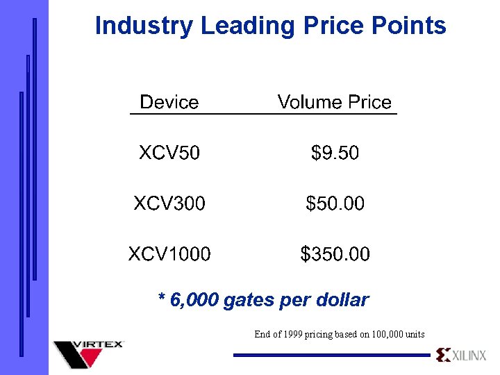
Industry Leading Price Points * 6, 000 gates per dollar End of 1999 pricing based on 100, 000 units

Virtex Testimonials Ad. Tech, Inc. "These million gate devices enable our test modules to provide thousands of continuous measurements at telecom speeds up to 2. 4 gigabits per second, " said Carl Uyehara, vice president of engineering at Adtech, Inc. , a leading supplier of broadband test systems. "We especially like the fact that Virtex devices are programmable. This allows us to use a single test module for multiple transmission technologies such as ATM and frame relay, which provides huge cost savings and convenience for our customers plus future enhancement capability. ” Carl Uyehara, vice president of Engineering Hughes Space and Communication Company "The critical features of Virtex, such as the segmented routing and 0. 22 micron feature size, allowed new levels of performance for our high-speed digital designs. The lower voltage and higher performance logic of the Virtex process are unmatched from any other supplier. The level of support from the design development and the hotline assistance that Xilinx offered with the new family also impressed us. ” Ted Pascaru, Senior Staff Engineer News Data Services (NDS) "Virtex FPGAs have allowed us to implement our next generation digital TV broadcast systems in record time. A key time saver was the availability of multiple DLLs that allowed us to synchronize a 74 MHz clock to more than 30 devices including multiple FPGAs, SDRAMs, and other components. Designing a no-skew clock system from scratch would take months. Xilinx delivered a ready-made solution to us with Virtex FPGAs. ” John Simmons, Project Manager Nortel Networks "In our next generation networking product, we specifically needed block RAM with true dual-port capabilities. We investigated various programmable solutions available and found that no other vendor could provide a single chip solution containing block memory with the ability to read and write to one port and simultaneously read from the other. Additionally, the Virtex DLLs performance was required in order to interface directly to an ASIC running at 78 MHz. Not only do Virtex devices meet our 78 MHz internal performance requirements, they meet our external interface performance requirements by providing very fast 'clock-to-out' timing on even the slowest device. ” Ranvir Chitkara, Director of Engineering

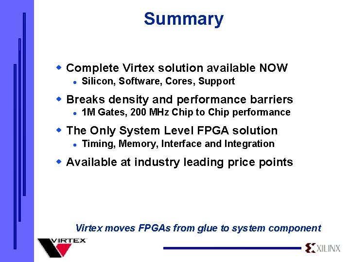
Summary w Complete Virtex solution available NOW l Silicon, Software, Cores, Support w Breaks density and performance barriers l 1 M Gates, 200 MHz Chip to Chip performance w The Only System Level FPGA solution l Timing, Memory, Interface and Integration w Available at industry leading price points Virtex moves FPGAs from glue to system component