Development of a Digital Temperature Transducer ASIC in

- Slides: 19
Development of a Digital Temperature Transducer ASIC in a 28 nm FD-SOI CMOS Process for a Spaceborne Low Power Sensor Bus P. P. Boraa, M. Ronerb, D. Borggrevea, A. Hurnib, E. Isaa, L. Maurerc a. Fraunhofer EMFT, Munich, Germany System AG, Oberpfaffenhofen, Germany c. Universität der Bundeswehr, Neubiberg, Germany b. OHB 13. 06. 2016 This work is funded through project THINGS 2 DO under the ENIAC grant agreement number 621221 and the national grant agreement number 16 ES 0240. © Fraunhofer
Agenda n Background n 28 nm FD-SOI Technology n System Requirements n System Description n Demonstrator n Conclusion © Fraunhofer 2
Agenda n Background n 28 nm FD-SOI Technology n System Requirements n System Description n Demonstrator n Conclusion © Fraunhofer 3
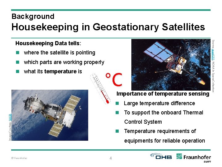
Background Housekeeping in Geostationary Satellites n where the satellite is pointing n which parts are working properly n what its temperature is °C Importance of temperature sensing n Large temperature difference Image Courtesy: NASA n To support the onboard Thermal © Fraunhofer Control System n Temperature requirements of equipments for reliable operation 4 Source: spac 0255, NOAA In Space Collection Housekeeping Data tells:
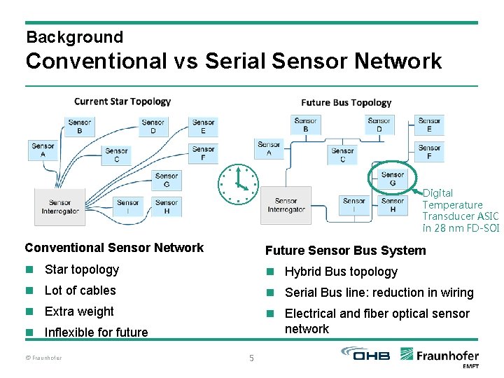
Background Conventional vs Serial Sensor Network Digital Temperature Transducer ASIC in 28 nm FD-SOI Conventional Sensor Network Future Sensor Bus System n Star topology n Hybrid Bus topology n Lot of cables n Serial Bus line: reduction in wiring n Extra weight n Electrical and fiber optical sensor network n Inflexible for future © Fraunhofer 5
Agenda n Background n 28 nm FD-SOI Technology n System Requirements n System Description n Demonstrator n Conclusion © Fraunhofer 6
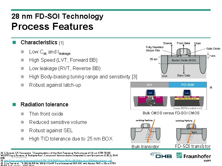
28 nm FD-SOI Technology Process Features n Characteristics [1] n Low Cds and Ileakage n High Speed (LVT, Forward BB) n Low leakage (RVT, Reverse BB) n High Body-biasing tuning range and sensitivity [3] n Robust against latch-up [2] n Radiation tolerance Image ©STMicroelectronics Bulk CMOS versus FD-SOI CMOS n Thin front oxide Ionizing Particle n Reduced sensitive volume n Robust against SEL Ionizing Particle BOX n High TID tolerance due to 25 nm BOX Bulk transistor [1] S. Shopov, S. P. Voinigescu, "Characterization of the High Frequency Performance of 28 -nm UTBB FDSOI MOSFETs as a Function of Backgate Bias", Compound Semiconductor Integrated Circuit Symposium (CSICs), 2014 © Fraunhofer IEEE [2] http: //cmp. imag. fr/documents/doc/UTBB-FDSOI%20 Design%20 and%20 Migration%20 Methodology_. pdf [3] S. Le Tual et al, “A 20 GHz-BW 6 b 10 GS/s 32 m. W Time-Interleaved SAR ADC with Master T&H in 28 nm UTBB 7 FD-SOI transistor
Agenda n Background n 28 nm FD-SOI Technology n System Requirements n System Description n Demonstrator n Conclusion © Fraunhofer 8
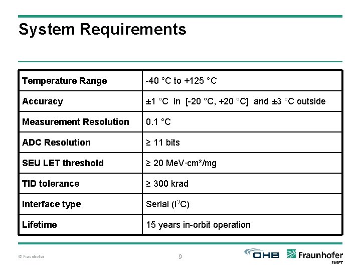
System Requirements Temperature Range -40 °C to +125 °C Accuracy ± 1 °C in [-20 °C, +20 °C] and ± 3 °C outside Measurement Resolution 0. 1 °C ADC Resolution ≥ 11 bits SEU LET threshold ≥ 20 Me. V∙cm²/mg TID tolerance ≥ 300 krad Interface type Serial (I 2 C) Lifetime 15 years in-orbit operation © Fraunhofer 9
Agenda n Background n 28 nm FD-SOI Technology n System Requirements n System Description n Demonstrator n Conclusion © Fraunhofer 10
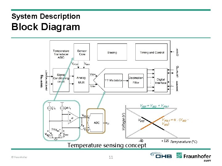
System Description Block Diagram Voltage (V) VREF = VBE 2 + VPTAT VBE 2 VPTAT = α. (VBE 2 VBE 1) -40 +125 Temperature (°C) Temperature sensing concept © Fraunhofer 11
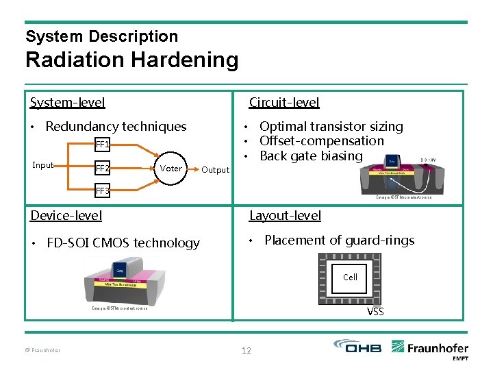
System Description Radiation Hardening System-level Circuit-level • Optimal transistor sizing • Offset-compensation • Back gate biasing • Redundancy techniques FF 1 Input FF 2 Voter Output FF 3 Image ©STMicroelectronics Device-level Layout-level • FD-SOI CMOS technology • Placement of guard-rings Cell VSS Image ©STMicroelectronics © Fraunhofer 12
Agenda n Background n 28 nm FD-SOI Technology n System Requirements n System Description n Demonstrator n Conclusion © Fraunhofer 13
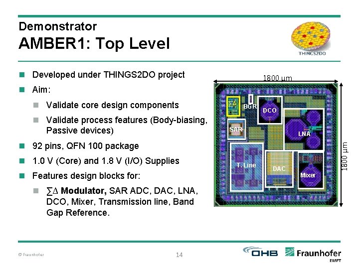
Demonstrator AMBER 1: Top Level n Developed under THINGS 2 DO project 1800 µm n Aim: n Validate core design components n Validate process features (Body-biasing, Passive devices) ∑∆ BGR DCO SAR LNA n 1. 0 V (Core) and 1. 8 V (I/O) Supplies n Features design blocks for: n ∑∆ Modulator, SAR ADC, DAC, LNA, DCO, Mixer, Transmission line, Band Gap Reference. © Fraunhofer 14 T. Line DAC 1800 µm n 92 pins, QFN 100 package Mixer
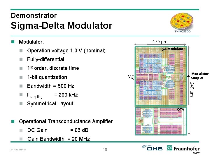
Demonstrator Sigma-Delta Modulator n Modulator: 159 µm ∑∆ Modulator n Operation voltage 1. 0 V (nominal) n Fully-differential n 1 st order, discrete time Modulator Output Vin+ n 1 -bit quantization - 249 µm n Bandwidth = 500 Hz n fsampling = 200 k. Hz n Symmetrical Layout OTA n Operational Transconductance Amplifier n DC Gain = 65 d. B n Gain Bandwidth = 20 MHz © Fraunhofer 15
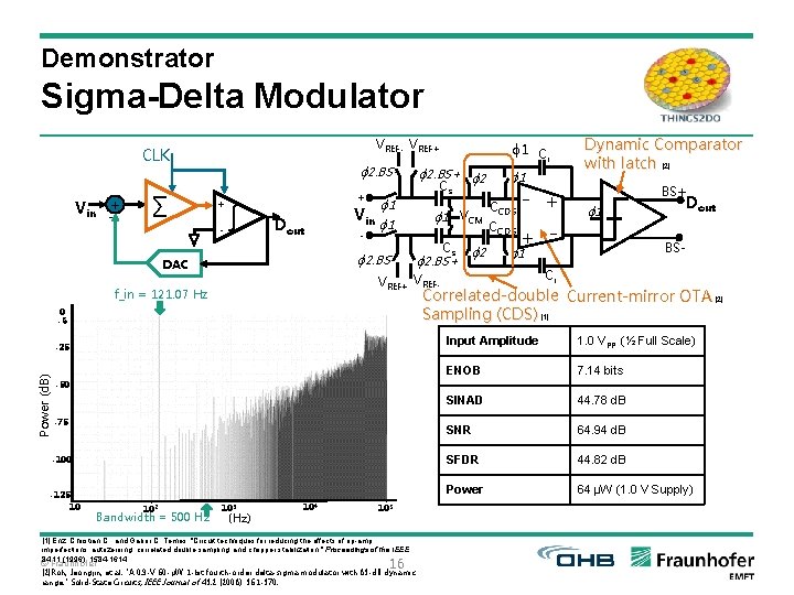
Demonstrator Sigma-Delta Modulator VREF- VREF+ CLK + Vin - ∑ ϕ 2. BS+ + - ∫ Dout Vin - ϕ 1 VREF+ f_in = 121. 07 Hz ϕ 1 VCM ϕ 1 ϕ 2. BS- DAC ϕ 2. BS+ ϕ 2 Cs Cs ϕ 2. BS+ VREF- 0 -6 - Power (d. B) -25 - -50 - -75 - Bandwidth = 500 Hz 103 (Hz) 104 - 102 - -12510 - ---100 - 105 [1] Enz, Christian C. , and Gabor C. Temes. "Circuit techniques for reducing the effects of op-amp imperfections: autozeroing, correlated double sampling, and chopper stabilization. " Proceedings of the IEEE 84. 11 (1996): 1584 -1614. © Fraunhofer 16 [2]Roh, Jeongjin, et al. "A 0. 9 -V 60 -μW 1 -bit fourth-order delta-sigma modulator with 83 -d. B dynamic range. " Solid-State Circuits , IEEE Journal of 43. 2 (2008): 361 -370. ϕ 1 C i ϕ 1 CCDS - + Dynamic Comparator with latch [2] BS+ ϕ 1 + - Dout BS- ϕ 1 Ci Correlated-double Current-mirror OTA [2] Sampling (CDS) [1] Input Amplitude 1. 0 VPP (½ Full Scale) ENOB 7. 14 bits SINAD 44. 78 d. B SNR 64. 94 d. B SFDR 44. 82 d. B Power 64 µW (1. 0 V Supply)
Agenda n Background n 28 nm FD-SOI Technology n System Requirements n System Description n Demonstrator n Conclusion © Fraunhofer 17
Conclusion n Digital Temperature Transducer ASIC: n Sensing, data-conversion and communication n 28 nm FDSOI CMOS Process: n Reduced parasitics, back-gate biasing, good radiation tolerance n System Requirements: n Up to ± 1 °C accuracy in [-20 °C, +20 °C] with 0. 1 °C resolution n Demonstrator: AMBER 1 IC n ∑∆ Modulator: 1 st order, discrete-time, correlated double sampling n Next Steps: n Validate 1 st order ∑∆ Modulator on AMBER 1 IC n Integrate sensor core and digital circuitry n Outlook: n Digital intensive design: exploit low-power features of 28 nm FD-SOI CMOS process n Further integration of components for space applications based on FD-SOI © Fraunhofer 18
THANK YOU © Fraunhofer