Chapter 1 Introduction to ASICs ApplicationSpecific Integrated Circuits
- Slides: 21

Chapter 1 Introduction to ASICs Application-Specific Integrated Circuits Michael John Sebastian Smith Addison Wesley, 1997 EGRE 427 Advanced Digital Design Figures from Application-Specific Integrated Circuits , Michael John Sebastian Smith, Addison Wesley, 1997

ASICs l ASIC - Application Specific Integrated Circuit n n l l Gate equivalent - a unit of size measurement corresponding to a 4 transistor gate equivalent (e. g. a 2 input NOR gate) Levels of integration: n n n l In Integrated Circuit (IC) designed to perform a specific function for a specific application As opposed to a standard, general purpose off-the-shelf part such as a commercial microprocessor or a 7400 series IC SSI - Small scale integration MSI - Medium scale integration LSI - Large scale integration VLSI - Very large scale integration USLI - Ultra large scale integration Implementation technology n n n TTL ECL MOS - NMOS, CMOS EGRE 427 Advanced Digital Design Figures from Application-Specific Integrated Circuits , Michael John Sebastian Smith, Addison Wesley, 1997

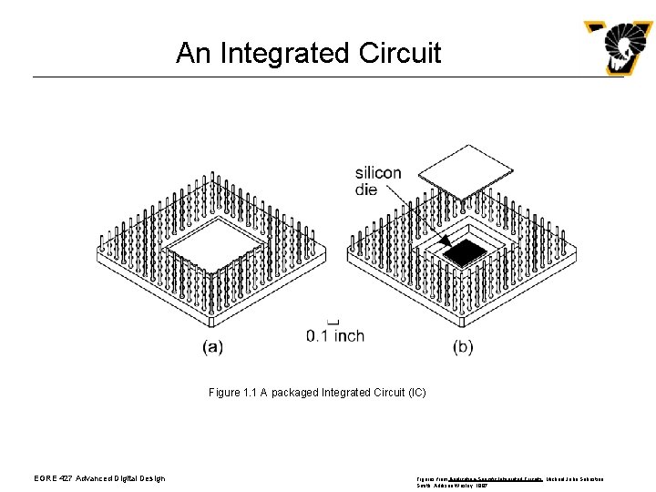
An Integrated Circuit Figure 1. 1 A packaged Integrated Circuit (IC) EGRE 427 Advanced Digital Design Figures from Application-Specific Integrated Circuits , Michael John Sebastian Smith, Addison Wesley, 1997

Types of ASICs l Full-Custom ASICs l Standard-Cell–Based ASICs l Gate-Array–Based ASICs l Channeled Gate Array l Channelless Gate Array l Structured Gate Array l Programmable Logic Devices l Field-Programmable Gate Arrays EGRE 427 Advanced Digital Design Figures from Application-Specific Integrated Circuits , Michael John Sebastian Smith, Addison Wesley, 1997

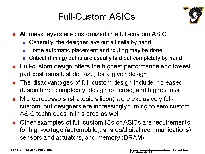
Full-Custom ASICs l All mask layers are customized in a full-custom ASIC n n n l l Generally, the designer lays out all cells by hand Some automatic placement and routing may be done Critical (timing) paths are usually laid out completely by hand Full-custom design offers the highest performance and lowest part cost (smallest die size) for a given design The disadvantages of full-custom design include increased design time, complexity, design expense, and highest risk Microprocessors (strategic silicon) were exclusively fullcustom, but designers are increasingly turning to semicustom ASIC techniques in this area as well Other examples of full-custom ICs or ASICs are requirements for high-voltage (automobile), analog/digital (communications), sensors and actuators, and memory (DRAM) EGRE 427 Advanced Digital Design Figures from Application-Specific Integrated Circuits , Michael John Sebastian Smith, Addison Wesley, 1997

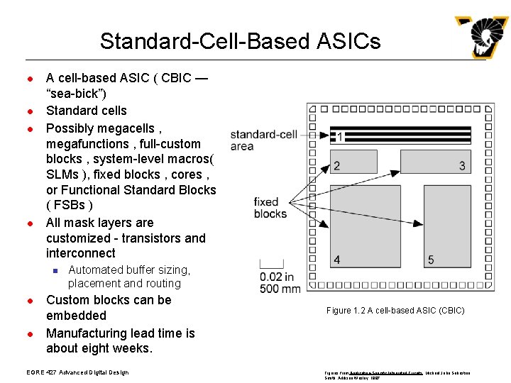
Standard-Cell-Based ASICs l l A cell-based ASIC ( CBIC — “sea-bick”) Standard cells Possibly megacells , megafunctions , full-custom blocks , system-level macros( SLMs ), fixed blocks , cores , or Functional Standard Blocks ( FSBs ) All mask layers are customized - transistors and interconnect n l l Automated buffer sizing, placement and routing Custom blocks can be embedded Manufacturing lead time is about eight weeks. EGRE 427 Advanced Digital Design Figure 1. 2 A cell-based ASIC (CBIC) Figures from Application-Specific Integrated Circuits , Michael John Sebastian Smith, Addison Wesley, 1997

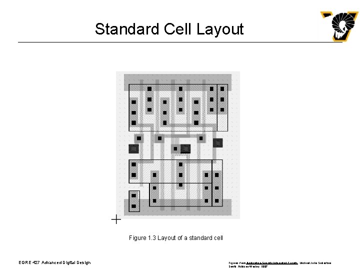
Standard Cell Layout Figure 1. 3 Layout of a standard cell EGRE 427 Advanced Digital Design Figures from Application-Specific Integrated Circuits , Michael John Sebastian Smith, Addison Wesley, 1997

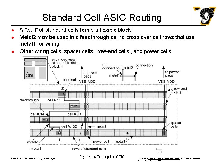
Standard Cell ASIC Routing l l l A “wall” of standard cells forms a flexible block Metal 2 may be used in a feedthrough cell to cross over cell rows that use metal 1 for wiring Other wiring cells: spacer cells , row-end cells , and power cells EGRE 427 Advanced Digital Design Figure 1. 4 Routing the CBIC Figures from Application-Specific Integrated Circuits , Michael John Sebastian Smith, Addison Wesley, 1997

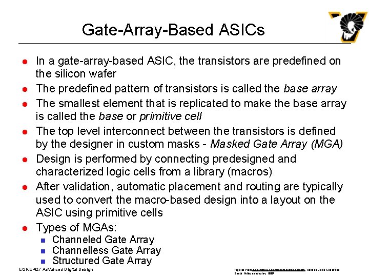
Gate-Array-Based ASICs l l l l In a gate-array-based ASIC, the transistors are predefined on the silicon wafer The predefined pattern of transistors is called the base array The smallest element that is replicated to make the base array is called the base or primitive cell The top level interconnect between the transistors is defined by the designer in custom masks - Masked Gate Array (MGA) Design is performed by connecting predesigned and characterized logic cells from a library (macros) After validation, automatic placement and routing are typically used to convert the macro-based design into a layout on the ASIC using primitive cells Types of MGAs: n n n Channeled Gate Array Channelless Gate Array Structured Gate Array EGRE 427 Advanced Digital Design Figures from Application-Specific Integrated Circuits , Michael John Sebastian Smith, Addison Wesley, 1997

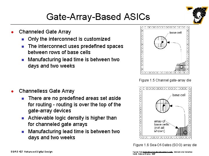
Gate-Array-Based ASICs l Channeled Gate Array n Only the interconnect is customized n The interconnect uses predefined spaces between rows of base cells n Manufacturing lead time is between two days and two weeks Figure 1. 5 Channel gate-array die l Channelless Gate Array n There are no predefined areas set aside for routing - routing is over the top of the gate-array devices n Achievable logic density is higher than for channeled gate arrays n Manufacturing lead time is between two days and two weeks Figure 1. 6 Sea-Of-Gates (SOG) array die EGRE 427 Advanced Digital Design Figures from Application-Specific Integrated Circuits , Michael John Sebastian Smith, Addison Wesley, 1997

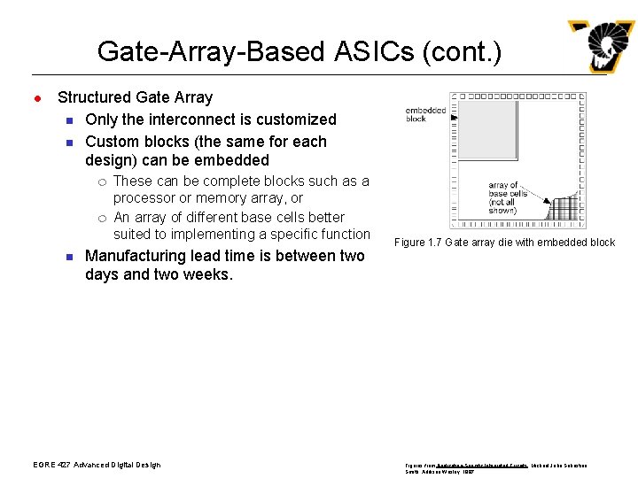
Gate-Array-Based ASICs (cont. ) l Structured Gate Array n Only the interconnect is customized n Custom blocks (the same for each design) can be embedded ¦ ¦ n These can be complete blocks such as a processor or memory array, or An array of different base cells better suited to implementing a specific function Manufacturing lead time is between two days and two weeks. EGRE 427 Advanced Digital Design Figure 1. 7 Gate array die with embedded block Figures from Application-Specific Integrated Circuits , Michael John Sebastian Smith, Addison Wesley, 1997

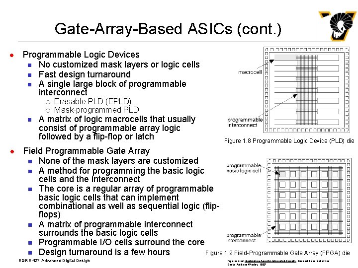
Gate-Array-Based ASICs (cont. ) l Programmable Logic Devices n No customized mask layers or logic cells n Fast design turnaround n A single large block of programmable interconnect ¦ ¦ n l Erasable PLD (EPLD) Mask-programmed PLD A matrix of logic macrocells that usually consist of programmable array logic followed by a flip-flop or latch Figure 1. 8 Programmable Logic Device (PLD) die Field Programmable Gate Array n None of the mask layers are customized n A method for programming the basic logic cells and the interconnect n The core is a regular array of programmable basic logic cells that can implement combinational as well as sequential logic (flipflops) n A matrix of programmable interconnect surrounds the basic logic cells n Programmable I/O cells surround the core n Design turnaround is a few hours Figure 1. 9 Field-Programmable Gate Array (FPGA) die EGRE 427 Advanced Digital Design Figures from Application-Specific Integrated Circuits , Michael John Sebastian Smith, Addison Wesley, 1997

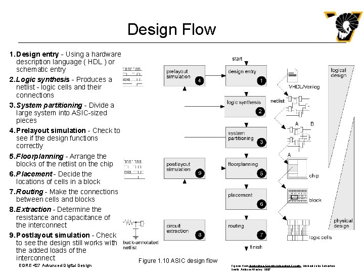
Design Flow 1. Design entry - Using a hardware description language ( HDL ) or schematic entry 2. Logic synthesis - Produces a netlist - logic cells and their connections 3. System partitioning - Divide a large system into ASIC-sized pieces 4. Prelayout simulation - Check to see if the design functions correctly 5. Floorplanning - Arrange the blocks of the netlist on the chip 6. Placement - Decide the locations of cells in a block 7. Routing - Make the connections between cells and blocks 8. Extraction - Determine the resistance and capacitance of the interconnect 9. Postlayout simulation - Check to see the design still works with the added loads of the interconnect EGRE 427 Advanced Digital Design Figure 1. 10 ASIC design flow Figures from Application-Specific Integrated Circuits , Michael John Sebastian Smith, Addison Wesley, 1997

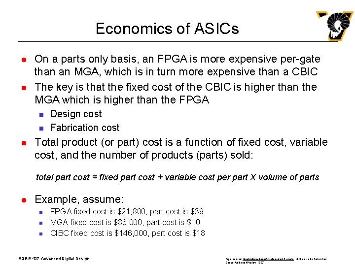
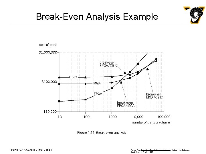
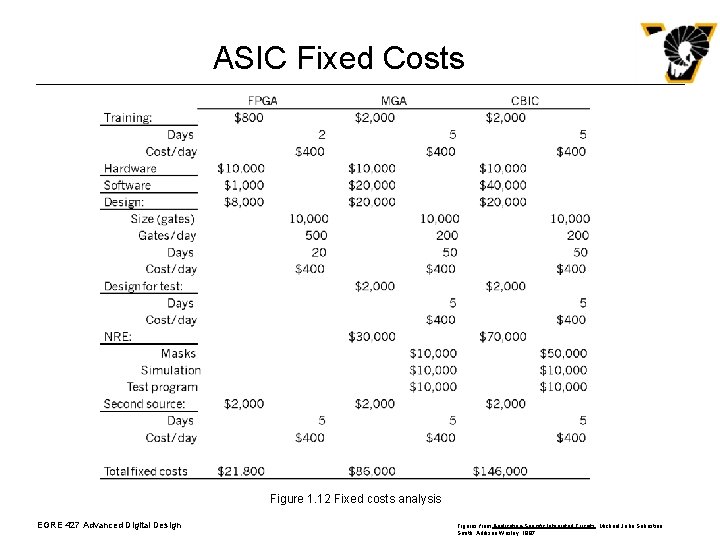
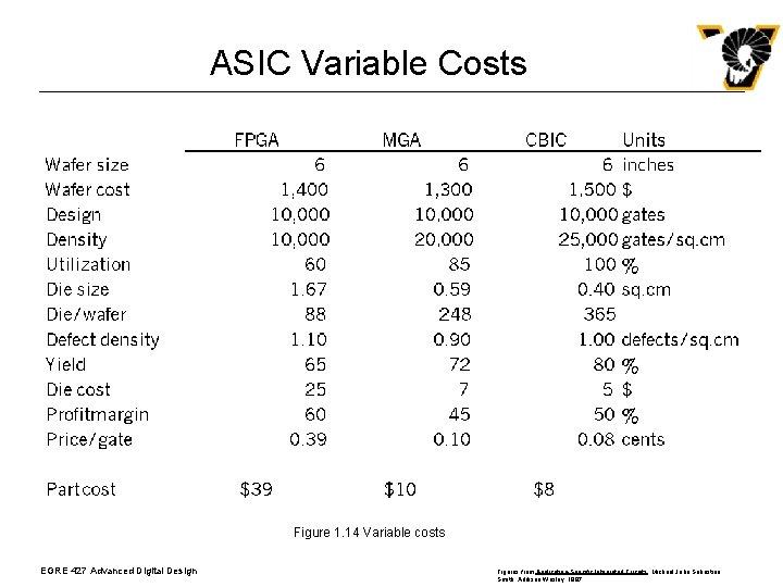
Economics of ASICs l l On a parts only basis, an FPGA is more expensive per-gate than an MGA, which is in turn more expensive than a CBIC The key is that the fixed cost of the CBIC is higher than the MGA which is higher than the FPGA n n l Design cost Fabrication cost Total product (or part) cost is a function of fixed cost, variable cost, and the number of products (parts) sold: total part cost = fixed part cost + variable cost per part X volume of parts l Example, assume: n n n FPGA fixed cost is $21, 800, part cost is $39 MGA fixed cost is $86, 000, part cost is $10 CIBC fixed cost is $146, 000, part cost is $18 EGRE 427 Advanced Digital Design Figures from Application-Specific Integrated Circuits , Michael John Sebastian Smith, Addison Wesley, 1997

Break-Even Analysis Example Figure 1. 11 Break even analysis EGRE 427 Advanced Digital Design Figures from Application-Specific Integrated Circuits , Michael John Sebastian Smith, Addison Wesley, 1997

ASIC Fixed Costs Figure 1. 12 Fixed costs analysis EGRE 427 Advanced Digital Design Figures from Application-Specific Integrated Circuits , Michael John Sebastian Smith, Addison Wesley, 1997

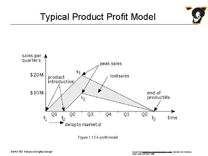
Typical Product Profit Model Figure 1. 13 A profit model EGRE 427 Advanced Digital Design Figures from Application-Specific Integrated Circuits , Michael John Sebastian Smith, Addison Wesley, 1997

ASIC Variable Costs Figure 1. 14 Variable costs EGRE 427 Advanced Digital Design Figures from Application-Specific Integrated Circuits , Michael John Sebastian Smith, Addison Wesley, 1997

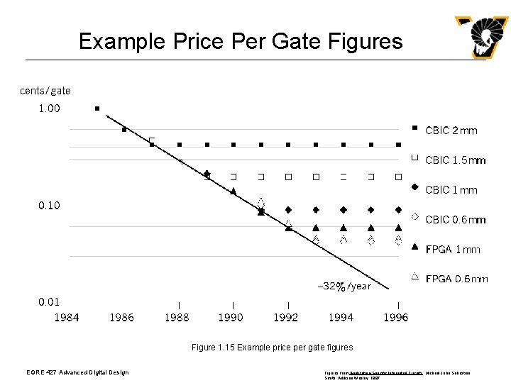
Example Price Per Gate Figures Figure 1. 15 Example price per gate figures EGRE 427 Advanced Digital Design Figures from Application-Specific Integrated Circuits , Michael John Sebastian Smith, Addison Wesley, 1997

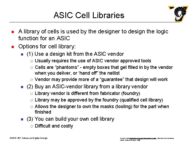
ASIC Cell Libraries l l A library of cells is used by the designer to design the logic function for an ASIC Options for cell library: n (1) Use a design kit from the ASIC vendor ¦ ¦ ¦ n (2) Buy an ASIC-vendor library from a library vendor ¦ ¦ ¦ n Usually requires the use of ASIC vendor approved tools Cells are “phantoms” - empty boxes that get filled in by the vendor when you deliver, or ‘hand off” the netlist Vendor may provide more of a “guarantee” that design will work Library vendor is different from fabricator (foundry) Library may be approved by the foundry (qualified cell library) Allows the designer to own the masks (tooling) for the part when finished (3) You can build your own cell library ¦ Difficult and costly EGRE 427 Advanced Digital Design Figures from Application-Specific Integrated Circuits , Michael John Sebastian Smith, Addison Wesley, 1997

ASIC Library Development l A complete ASIC library (suitable for commercial use) must include the following for each cell and macro: n n n n n A physical layout A behavioral model A VHDL or Verilog model A detailed timing model A test strategy A circuit schematic A cell icon (symbol) A wire-load model A routing model EGRE 427 Advanced Digital Design Figures from Application-Specific Integrated Circuits , Michael John Sebastian Smith, Addison Wesley, 1997