
PLD Basics September 00 1 Agenda Basic Logic
PLD Basics September, 00 1
Agenda Basic Logic Tutorial Gal / Architecture CPLD / Architecture ISP Software Packaging September, 00 2
Digital Logic Tutorial September, 00 3
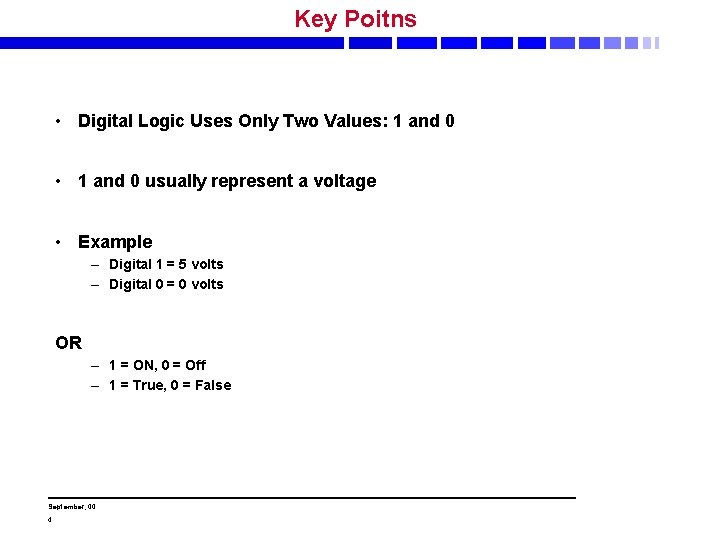
Key Poitns • Digital Logic Uses Only Two Values: 1 and 0 • 1 and 0 usually represent a voltage • Example – Digital 1 = 5 volts – Digital 0 = 0 volts OR – 1 = ON, 0 = Off – 1 = True, 0 = False September, 00 4
Boolean Basics • Manipulation of digital values is done by Boolean Algebra • Boolean algebra uses primarily AND / OR functions • Boolean equation: TRUE OR FALSE = TRUE • Programmable logic implements the AND / OR functions in hardware September, 00 5
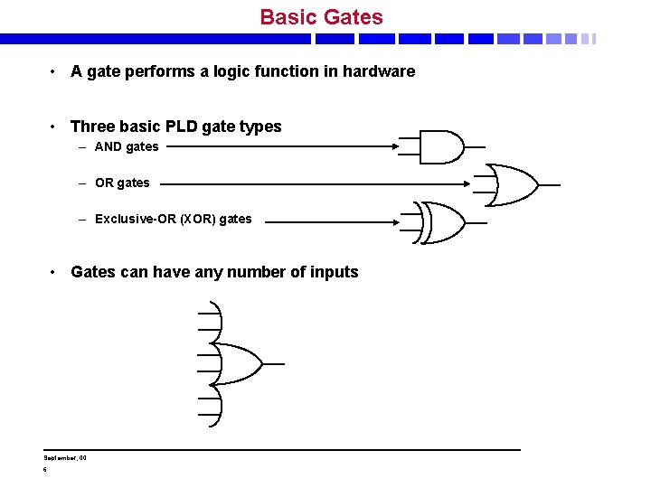
Basic Gates • A gate performs a logic function in hardware • Three basic PLD gate types – AND gates – OR gates – Exclusive-OR (XOR) gates • Gates can have any number of inputs September, 00 6
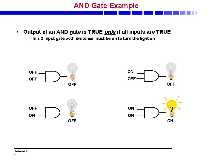
AND Gate Example • Output of an AND gate is TRUE only if all inputs are TRUE – In a 2 input gate both switches must be on to turn the light on OFF ON OFF OFF OFF ON ON ON OFF September, 00 7 ON
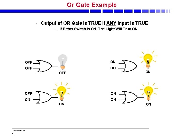
Or Gate Example • Output of OR Gate Is TRUE if ANY Input is TRUE – If Either Switch Is ON, The Light Will Trun ON OFF OFF OFF ON ON September, 00 8 ON ON
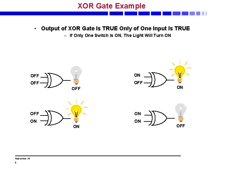
XOR Gate Example • Output of XOR Gate Is TRUE Only of One Input Is TRUE – If Only One Switch Is ON, The Light Will Turn ON OFF OFF OFF ON ON September, 00 9 ON OFF
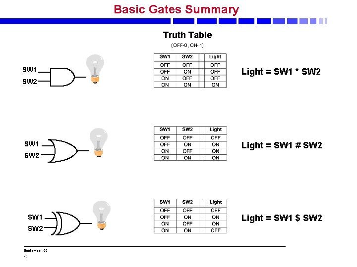
Basic Gates Summary Truth Table (OFF-0, ON-1) SW 1 Light = SW 1 * SW 2 SW 1 Light = SW 1 # SW 2 SW 1 SW 2 September, 00 10 Light = SW 1 $ SW 2
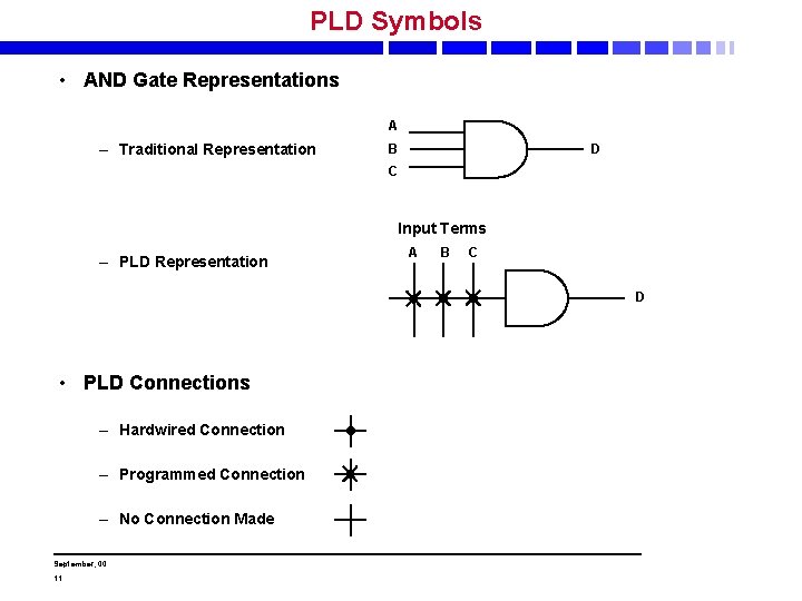
PLD Symbols • AND Gate Representations A – Traditional Representation B D C Input Terms – PLD Representation A B C D • PLD Connections – Hardwired Connection – Programmed Connection – No Connection Made September, 00 11
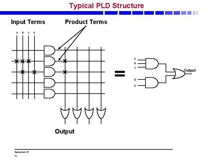
Typical PLD Structure Input Terms A B C Product Terms D A B C B D Output September, 00 12 Output
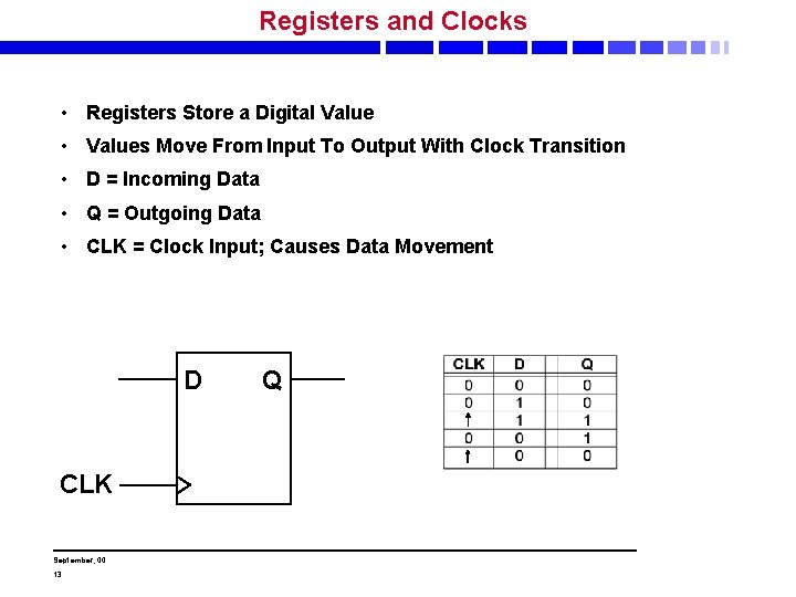
Registers and Clocks • Registers Store a Digital Value • Values Move From Input To Output With Clock Transition • D = Incoming Data • Q = Outgoing Data • CLK = Clock Input; Causes Data Movement D CLK September, 00 13 Q
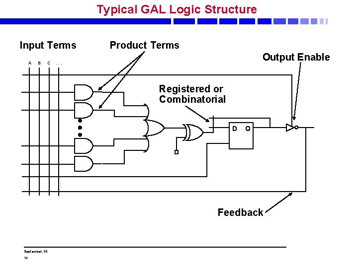
Typical GAL Logic Structure Input Terms A B C Product Terms Output Enable . . . Registered or Combinatorial D Q Feedback September, 00 14
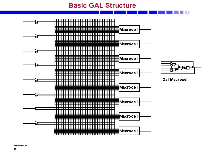
Basic GAL Structure Macrocell Gal Macrocell Macrocell September, 00 15
GAL Devices • Low density GAL product families: 16/20 V 8, 18/22 V 10/26 V 12, 20 RA 10, 20 XV 10, 6001/6002. Families are organized based on architectural layout and a common Output Logic Macro Cell (OLMC). Pin counts and array sizes are all that change across a family. • Lattice GAL devices have Macro Cell counts from 8 to 39 and package sizes from 20 pins to 28 pins. • All GAL devices have registered or combinatorial options, OE control, and selectable output polarity. September, 00 16
GAL Devices • There also various flavors of each device type. – – – An L in the product name is a low voltage (3. 3 V) device. Zero power devices are either Z or ZD, such as 22 LV 10 ZD. A VP indicates high drive outputs, such as the 16 VP 8. The isp. GAL 16 Z 8 was the worlds first ISP PLD. There is also a Confusion Letter, which roughly indicates the process and technology that the device is based on. • Appended to each device type are speed, power, package, etc. – Device speed grades are by TPD in ns. (HD devices are graded by Fmax in MHz. ) – Power dissipation (standard, Low, and Quarter), package type (Pdip, Jlcc, Soic), and Temp/VCC range are appended to device names such as 16 LV 8 C-5 LJI for 5 n. S, low power, PLCC, Industrial. September, 00 17
PAL Vs. GAL • PAL: – Programmable Array Logic. – Registers, feedback paths, dynamic I/O, and both output polarities are available. – There are dozens of different devices each with a fixed architecture. For example, a PAL 16 H 2 has 16 inputs and 2 combinatorial outputs each with 8 PTs per OR gate. Output polarity is positive. • GAL: – Generic Array Logic. – GALs are a superset of PALs. A few GAL devices cover all PAL architectures and hundreds of other possible configurations. – GALs add extremely flexible routing and complete reconfigurability. – The structure of GAL devices allows them to replace many PALs with various IO, input and register counts. Therefore, extra programmable areas known as architecture rows are needed for device configuration. There are global configuration modes and well as individual Macro. Cell options. September, 00 18
High Density Logic Overview September, 00 19
isp. LSI Heritage • The isp. LSI Architecture Has Its Origins In The GAL Family • The Best Features Of The GAL Family Have Been Blended Toghter – – – September, 00 20 GAL 16 V 8: GAL 22 V 10 GAL 20 XV 10 GAL 20 RA 10 GAL 6002: Output Logic Macrocell (OLMC) More Product Terms Exclusive OR Gate (XOR) Asynchronous Clocking Input Registers and Product Term Sharing
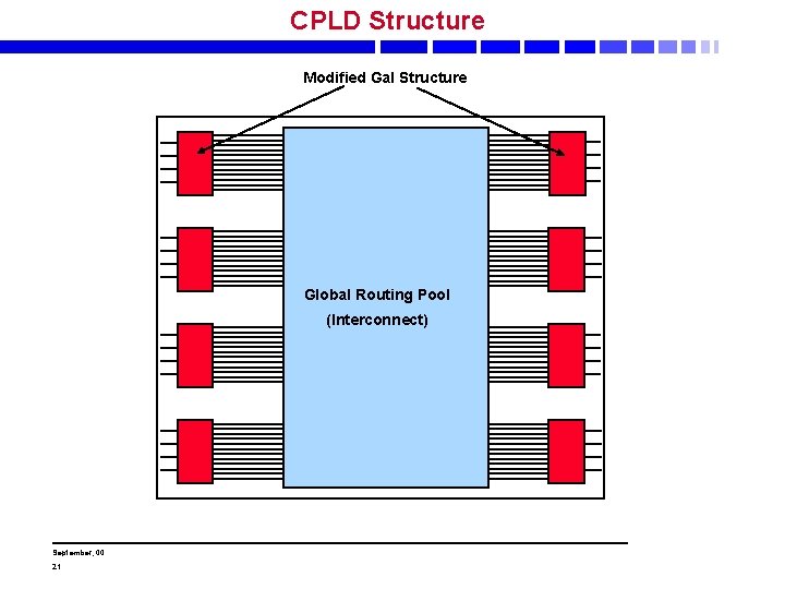
CPLD Structure Modified Gal Structure Global Routing Pool (Interconnect) September, 00 21
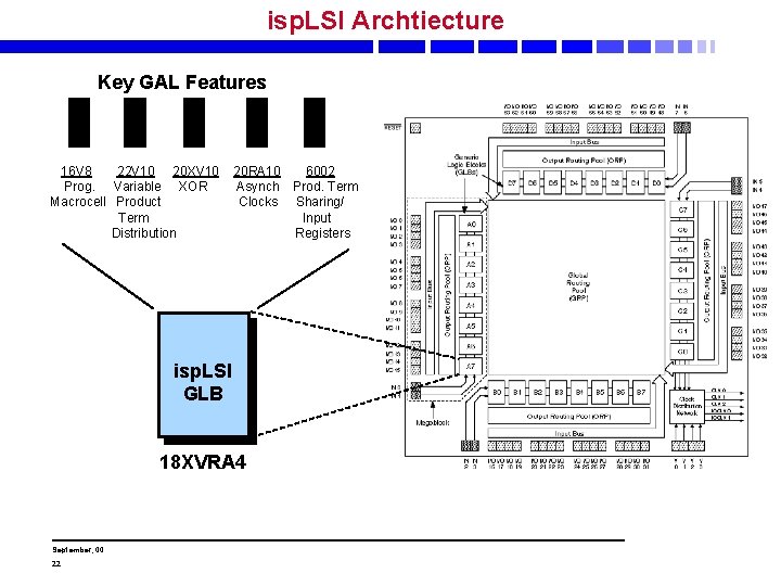
isp. LSI Archtiecture Key GAL Features 16 V 8 22 V 10 20 XV 10 Prog. Variable XOR Macrocell Product Term Distribution 20 RA 10 Asynch Clocks isp. LSI GLB 18 XVRA 4 September, 00 22 6002 Prod. Term Sharing/ Input Registers
High Density Structure • Simple Lattice definition: High Density (HD) devices are those with 1000 or more PLD gates and packages exceeding 28 pins. Our HD devices are Complex PLDs (CPLDs). • HD devices are essentially many identical GAL sized blocks that are repeated to form larger devices. • There is a portion of the device dedicated to routing signals between logic blocks called the Global Routing Pool (GRP) • In GAL terms, the basic GLB (1 K, 2 K families) is a fancy 18 V 4. – The logic in the GLB contains most of the features available in the entire GAL family, but on a smaller, more limited scale. » PT clocking » XOR functions » 20 wide OR » PT reset – Much of the logic is mutually exclusive and gets ‘burned’ as other logic is used. This is overcome by having many GLBs. September, 00 23
High Density Structure • Megablock/Megacell based. – A Megablock contains 8 GLBs. – Devices in a family are built from whole Megablocks. • The Global Routing Pool (GRP) is the only means to get signals from one GLB to the next and to get the IO cells to the GLBs. • External pins such as CLK pins, RESET, and GOE are globally fed to all GLBs. • The only other global signals are internally generated clocks and OE’s (differ by family and device). September, 00 24
CPLDs and FPGAs September, 00 25
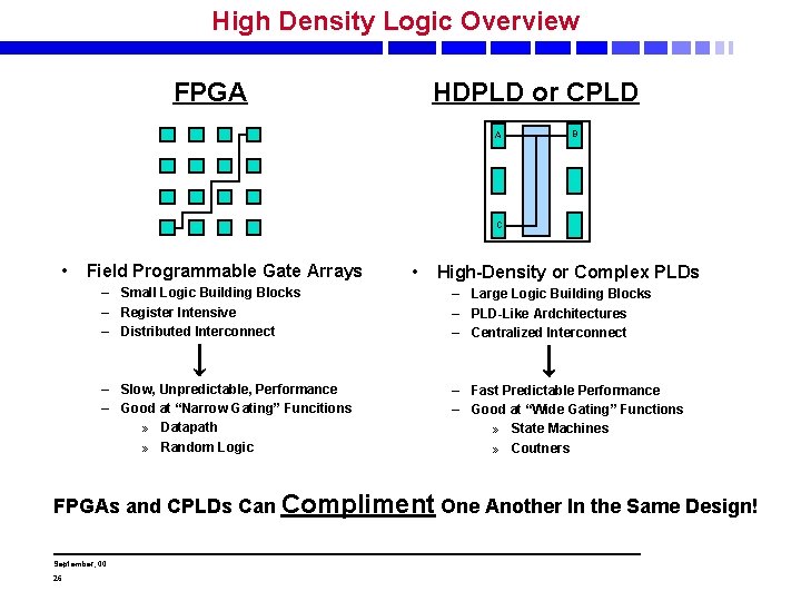
High Density Logic Overview FPGA HDPLD or CPLD A B C • Field Programmable Gate Arrays • High-Density or Complex PLDs – Small Logic Building Blocks – Register Intensive – Distributed Interconnect – Large Logic Building Blocks – PLD-Like Ardchitectures – Centralized Interconnect – Slow, Unpredictable, Performance – Good at “Narrow Gating” Funcitions » Datapath » Random Logic – Fast Predictable Performance – Good at “Wide Gating” Functions » State Machines » Coutners FPGAs and CPLDs Can Compliment One Another In the Same Design! September, 00 26
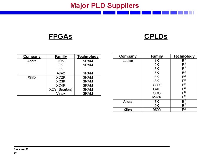
Major PLD Suppliers FPGAs September, 00 27 CPLDs
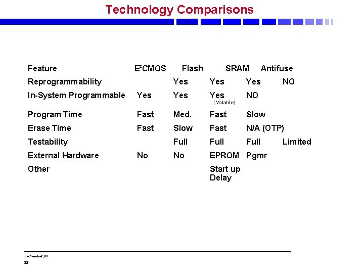
Technology Comparisons Feature E 2 CMOS Reprogrammability Flash SRAM Antifuse Yes Yes NO In-System Programmable Yes Yes NO Program Time Fast Med. Fast Slow Erase Time Fast Slow Fast N/A (OTP) Full No EPROM Pgmr Testability External Hardware Other September, 00 28 No (Volatile) Start up Delay Limited
The GDX September, 00 29
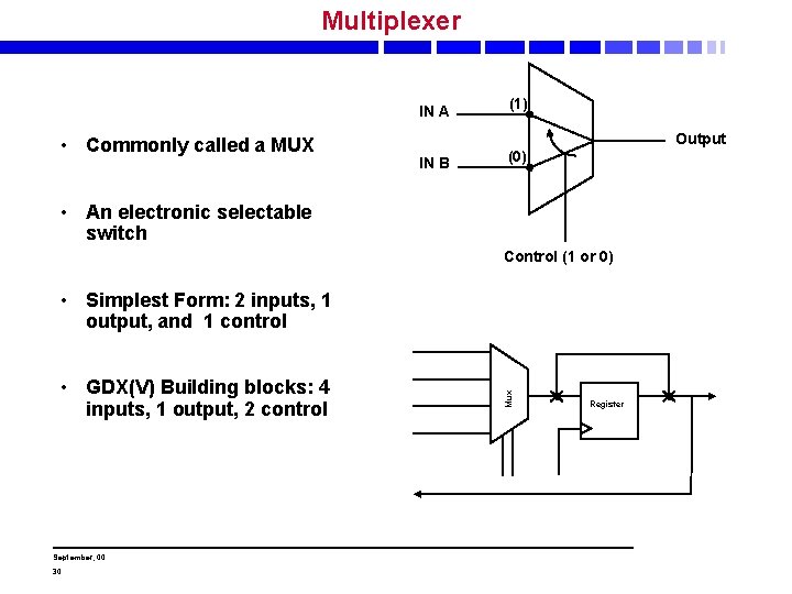
Multiplexer IN A • Commonly called a MUX (1) Output IN B (0) • An electronic selectable switch Control (1 or 0) • GDX(V) Building blocks: 4 inputs, 1 output, 2 control September, 00 30 Mux • Simplest Form: 2 inputs, 1 output, and 1 control Register
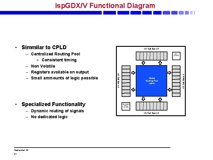
isp. GDX/V Functional Diagram • Simmilar to CPLD • Specialized Functionality – Dynamic routing of signals – No dedicated logic September, 00 31 Global Routing Pool (GRP) Boundary Scan Control I/O Cell Bank B I/O Cell Bank A ISP Control I/O Cell Bank A – Centralized Routing Pool » Consistent timing – Non Volatile – Registers available on output – Small ammounts of logic possible I/O Cell Bank D
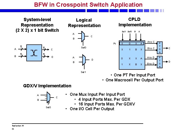
BFW in Crosspoint Switch Application System-level Representation (2 X 2) x 1 bit Switch CPLD Implementation Logical Representation Sel 1 Sel 0 A Pt B 1 1 Sel 0 C D A D B Sel 1 C B Sel 0 September, 00 32 A to C X 0 X A X 1 B X 0 X X A A to D 1 X B to D B to C P T S A D • One PT Per Input Port • One Macrocell Per Output Port GDX/V Implementation A A C B A B • One Mux Input Per Input Port • 4 Input Ports Max. Per GDX • 16 Input Ports Max. Per GDXV • One I/O Cell Per Output
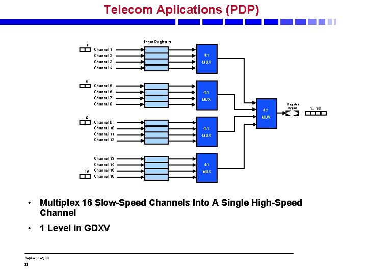
Telecom Aplications (PDP) 1 5 Input Registers Channel 1 Channel 2 Channel 3 Channel 4 Channel 5 Channel 6 Channel 7 Channel 8 4: 1 MUX 4: 1 9 16 Register Bypass MUX Channel 9 Channel 10 Channel 11 Channel 12 Channel 13 Channel 14 Channel 15 Channel 16 4: 1 MUX • Multiplex 16 Slow-Speed Channels Into A Single High-Speed Channel • 1 Level in GDXV September, 00 33 1… 16
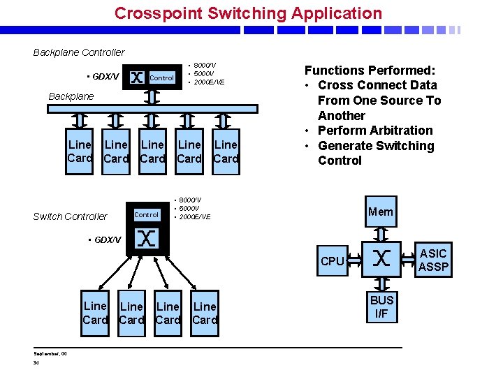
Crosspoint Switching Application Backplane Controller • GDX/V • 8000/V • 5000 V • 2000 E/VE Control Backplane Line Card Switch Controller Line Card Control Line Card Functions Performed: • Cross Connect Data From One Source To Another • Perform Arbitration • Generate Switching Control • 8000/V • 5000 V • 2000 E/VE Mem • GDX/V ASIC ASSP CPU Line Card September, 00 34 Line Card BUS I/F
In-System-Programmable (ISP) September, 00 35
Historical Programming Originally all programming had to be done in a separate piece of hardware • One Time Programmable (OTP) – Antifuse technology – Not erasable • Erasable PLDs (EPLDs) – UV light used to erase device – Expensive packaging • Electrically Erasable PLDs – Could be erased by programming equipment – Had to be removed from circuit for both programming and erasing – Uses High (~12 v) voltages to program September, 00 36
In-System-Programming • ISP PLDs – Programming and erasing done through a wire interface to the part » Programming voltages generated “on chip” – Part can be soldered to the board » No need to handle parts » More delicate (smaller) packaging can be used – Field upgrades are possible – Multiple / different devices can be programmed at once September, 00 37
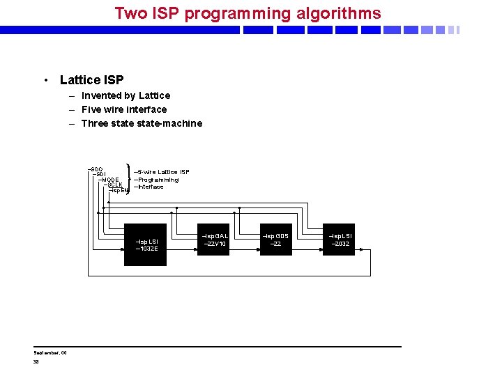
Two ISP programming algorithms • Lattice ISP – Invented by Lattice – Five wire interface – Three state-machine –SDO –SDI –MODE –SCLK –isp. EN – 5 -wire Lattice ISP –Programming –Interface –isp. LSI – 1032 E September, 00 38 –isp. GAL – 22 V 10 –isp. GDS – 22 –isp. LSI – 2032
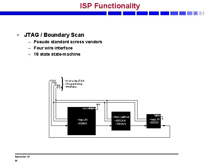
ISP Functionality • JTAG / Boundary Scan – Pseudo standard across vendors – Four wire interface – 16 state-machine –TDO – 4 -wire isp. JTAG –TDI –Programming –TMS –TCK –Interface –VCC –BSCAN/isp. EN –isp. LSI – 3256 A September, 00 39 –Non-Lattice –BSCAN –Device –isp. EN –isp. LSI – 2032 V
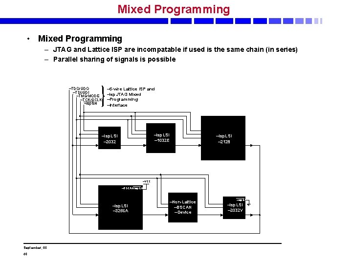
Mixed Programming • Mixed Programming – JTAG and Lattice ISP are incompatable if used is the same chain (in series) – Parallel sharing of signals is possible –TDO/SDO –TDI/SDI –TMS/MODE –TCK/SCLK –isp. EN – 5 -wire Lattice ISP and –isp. JTAG Mixed –Programming –Interface –isp. LSI – 1032 E –isp. LSI – 2032 –isp. LSI – 2128 –VCC –BSCAN/isp. EN –isp. LSI – 3256 A September, 00 40 –Non-Lattice –BSCAN –Device –isp. EN –isp. LSI – 2032 V
ISP Innovator and Market Leader September, 00 41
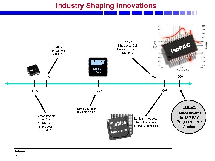
Industry Shaping Innovations Lattice introduces Cell Based PLD with Memory Lattice introduces the ISP GAL isp. LSI 1000 1986 1985 1997 1992 TODAY Lattice invents the ISP CPLD Lattice invents the GAL Architecture; introduces E 2 CMOS September, 00 42 1999 1996 Lattice Introduces the ISP Generic Digital Crosspoint Lattice Invents the ISP PAC Programmable Analog
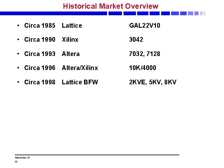
Historical Market Overview • Circa 1985 Lattice GAL 22 V 10 • Circa 1990 Xilinx 3042 • Circa 1993 Altera 7032, 7128 • Circa 1996 Altera/Xilinx 10 K/4000 • Circa 1998 Lattice BFW 2 KVE, 5 KV, 8 KV September, 00 43
Company Background • Lattice is the Inventor of In-System-Programmable PLDs • The PLD Performance Leader • World’s Largest Supplier of ISP PLDs • Fastest Growing CPLD Supplier • Broadest Line Supplier September, 00 44
Lattice Device Packages September, 00 45
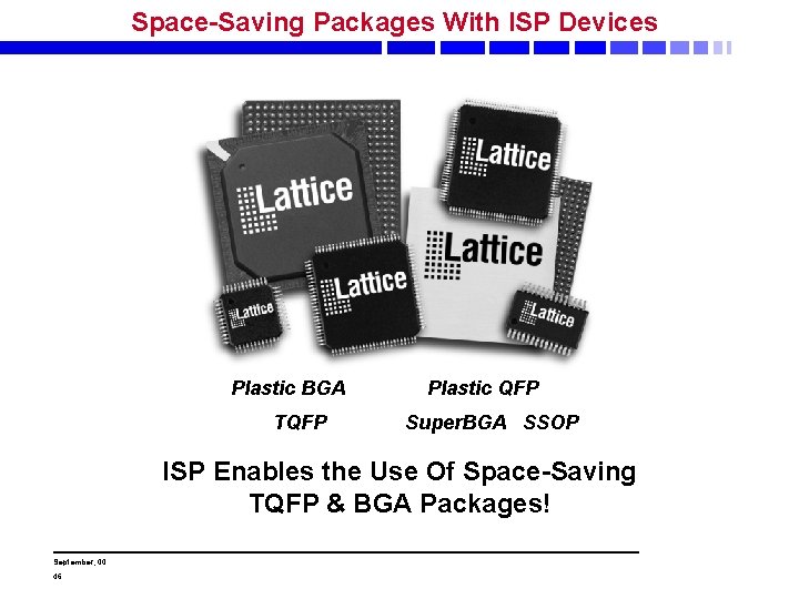
Space-Saving Packages With ISP Devices Plastic BGA TQFP Plastic QFP Super. BGA SSOP ISP Enables the Use Of Space-Saving TQFP & BGA Packages! September, 00 46
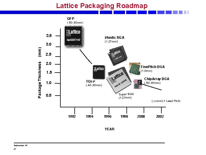
Lattice Packaging Roadmap QFP (. 50 -. 80 mm) 3. 5 Plastic BGA (1. 27 mm) Package Thickness (mm) 3. 0 2. 5 2. 0 Fine. Pitch BGA (1. 0 mm) 1. 5 Chip. Array BGA TQFP 1. 0 (. 50 -. 80 mm) (. 40 -. 80 mm) Super BGA (1. 27 mm) 0. 5 (. xxmm) = Lead Pitch 1992 1994 1996 YEAR September, 00 47 1998 2000 2002
Software Basics September, 00 48
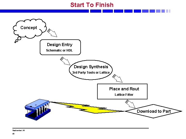
Start To Finish Concept Design Entry Schematic or HDL Design Synthesis 3 rd Party Tools or Lattice Place and Rout Lattice Fitter Download to Part September, 00 49
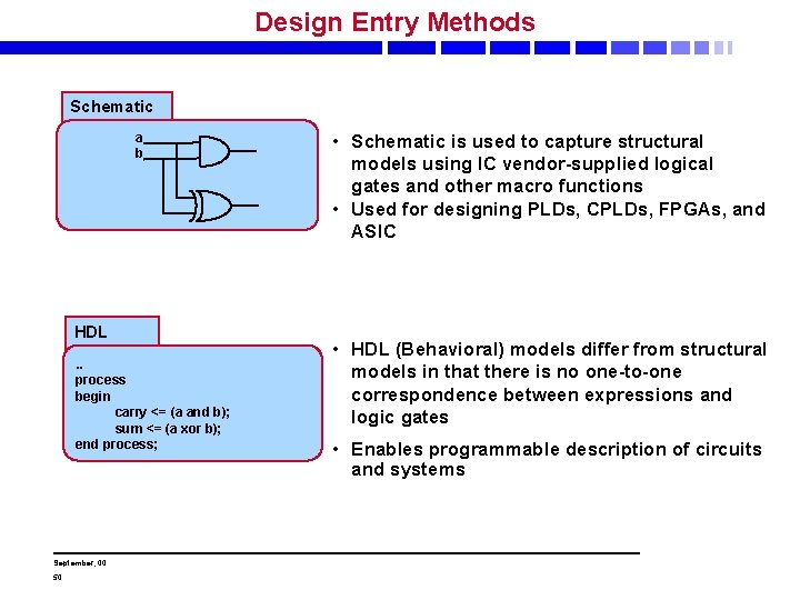
Design Entry Methods Schematic a b HDL. . process begin carry <= (a and b); sum <= (a xor b); end process; September, 00 50 • Schematic is used to capture structural models using IC vendor-supplied logical gates and other macro functions • Used for designing PLDs, CPLDs, FPGAs, and ASIC • HDL (Behavioral) models differ from structural models in that there is no one-to-one correspondence between expressions and logic gates • Enables programmable description of circuits and systems
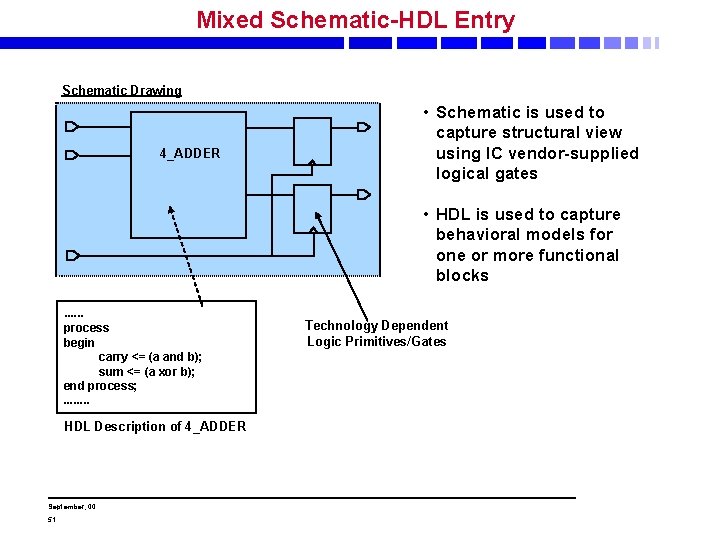
Mixed Schematic-HDL Entry Schematic Drawing 4_ADDER • Schematic is used to capture structural view using IC vendor-supplied logical gates • HDL is used to capture behavioral models for one or more functional blocks . . . process begin carry <= (a and b); sum <= (a xor b); end process; . . . . HDL Description of 4_ADDER September, 00 51 Technology Dependent Logic Primitives/Gates
Schematic-Based Design Methodology September, 00 52
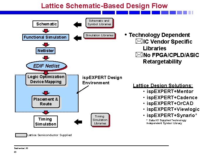
Lattice Schematic-Based Design Flow Schematic Functional Simulation Schematic and Symbol Libraries Simulation Libraries *No FPGA/CPLD/ASIC Retargetability Netlister EDIF Netlist Logic Optimization Device Mapping isp. EXPERT Design Environment Placement & Route Timing Simulation Lattice Semiconductor Supplied September, 00 53 • Technology Dependent *IC Vendor Specific Timing Simulation Libraries Lattice Design Solutions: • isp. EXPERT+Mentor • isp. EXPERT+Cadence • isp. EXPERT+Or. CAD • isp. EXPERT+Viewlogic • isp. EXPERT+Synario* * Data I/O Supplied Technology Independent Symbol Library
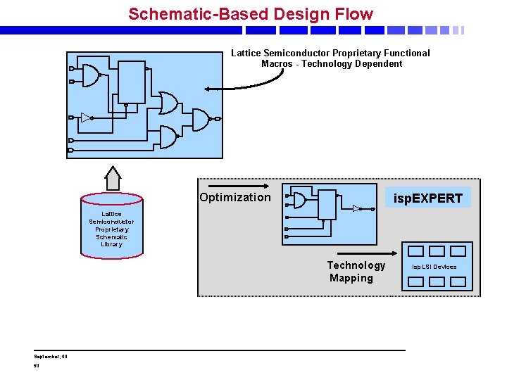
Schematic-Based Design Flow Lattice Semiconductor Proprietary Functional Macros - Technology Dependent Optimization isp. EXPERT Lattice Semiconductor Proprietary Schematic Library Technology Mapping September, 00 54 isp. LSI Devices
HDL-Based Design Methodology September, 00 55
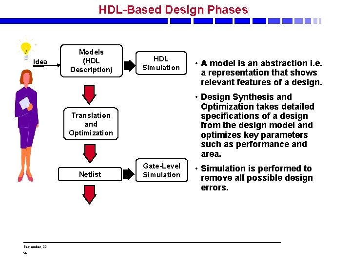
HDL-Based Design Phases Idea Models (HDL Description) HDL Simulation • Design Synthesis and Optimization takes detailed specifications of a design from the design model and optimizes key parameters such as performance and area. Translation and Optimization Netlist September, 00 56 • A model is an abstraction i. e. a representation that shows relevant features of a design. Gate-Level Simulation • Simulation is performed to remove all possible design errors.
What is HDL? • Hardware Description Language. The term model in HDL is analogous to the term program in software. • Language that enables description of circuits and systems • Examples: – Verilog-HDL - Verilog-HDL is a hardware description language (Cadence/OVI Standard) which provides a means of specifying a digital system at a wide range of levels of abstraction. – VHDL - Acronym for VHSIC hardware description language (ANSI/IEEE Standard). VHDL is a hardware description language which provides a means of specifying a digital system at a wide range of levels of abstraction. – Abel - Originally from Data I/O September, 00 57
Design Synthesis • HDL Synthesis - Transformations of HDL Models to microscopic (i. e. , gate-level) structure of a design. • Logic Synthesis - Consists of two separate phases called Logic Optimization and Technology Mapping. – Logic Optimization - The role of optimization is to enhance the overall quality of the design, such as performance and area. – Technology Mapping - Transformation of the optimized design into a design that consists of restricted set of elements. In the CPLD environment, the elements are I/O and GLB cells. September, 00 58
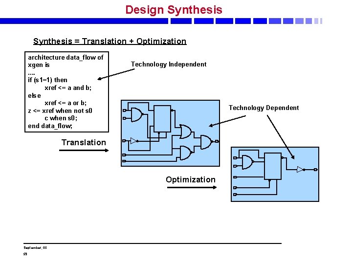
Design Synthesis = Translation + Optimization architecture data_flow of xgen is. . if (s 1=1) then xref <= a and b; else xref <= a or b; z <= xref when not s 0 c when s 0; end data_flow; Technology Independent Technology Dependent Translation Optimization September, 00 59

Lattice HDL-Based Design Flow VHDL/Verilog-HDL Description VHDL/Verilog Simulation Synthesis Functional Simulation Libraries Synthesis Libraries • Supports Top-Down Design Methodologies EDIF Netlist Logic Optimization Device Mapping isp. EXPERT Design Environment Placement & Route Verilog/VHDL Timing Simulation Lattice Semiconductor Supplied September, 00 60 • Technology Independent; FPGA/CPLD/ASIC Retargetability Timing Simulation Libraries Lattice Design Solutions: • isp. EXPERT+Viewlogic • isp. EXPERT+Mentor • isp. EXPERT+Cadence • isp. EXPERT+Synopsys • isp. EXPERT+Exemplar
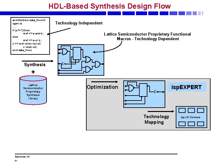
HDL-Based Synthesis Design Flow architecture data_flow of xgen is. . if (s 1=1) then xref <= a and b; else xref <= a or b; z <= xref when not s 0 c when s 0; end data_flow; Technology Independent Lattice Semiconductor Proprietary Functional Macros - Technology Dependent Synthesis + Lattice Semiconductor Proprietary Synthesis Library Optimization isp. EXPERT Technology Mapping September, 00 61 isp. LSI Devices
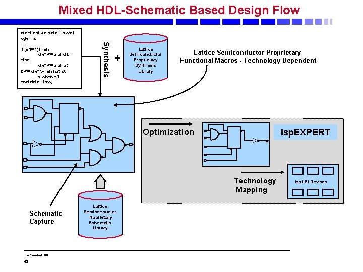
Mixed HDL-Schematic Based Design Flow Synthesis architecture data_flow of xgen is. . if (s 1=1) then xref <= a and b; else xref <= a or b; z <= xref when not s 0 c when s 0; end data_flow; + Lattice Semiconductor Proprietary Synthesis Library Lattice Semiconductor Proprietary Functional Macros - Technology Dependent isp. EXPERT Optimization Technology Mapping Schematic Capture September, 00 62 Lattice Semiconductor Proprietary Schematic Library isp. LSI Devices
Design Verification Overview Design Verification (Simulation) is performed to remove all possible design errors Types Of Design Verification and Their Definitions • Technology Independent Functional Simulation – Performed Prior to Design Synthesis or Compilation – Verifies Only That The Design Performs As Logically Expected • Technology Dependent Functional Simulation – Performed After Design Synthesis Or Compilation and Targeted Toward a Specific Silicon technology – Verifies Only That The Design Performs as Logically Expected • Technology Dependent Timing Simulation – Performed after Device Fitting / Compilation and Targeted Toward A Specific Silicon Technology. – Verifies That Both Logic AND Timing Requirements For The design Have Been Met September, 00 63
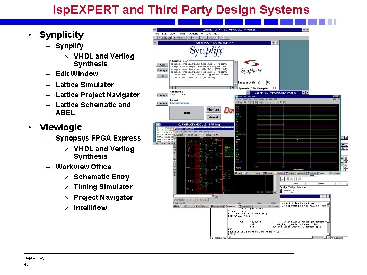
isp. EXPERT and Third Party Design Systems • Synplicity – Synplify » VHDL and Verilog Synthesis – Edit Window – Lattice Simulator – Lattice Project Navigator – Lattice Schematic and ABEL • Viewlogic – Synopsys FPGA Express » VHDL and Verilog Synthesis – Workview Office » Schematic Entry » Timing Simulator » Project Navigator » Intelliflow September, 00 64
Download Software Lattice Provides Several Methods of Programming Parts • ISP Code – Allows a Microprocessor to program device directly • ISP VM (Virtual Machine) – Software That Can Program Lattice Devices As Well As Our Comptetitor • ISP ATE (Automated Test Equipment) – Allows The Customers Test Equipment To Program Our Device • Turbo Download – Allows Multiple - Different Lattice Devices to be Programmed Simultaneously • ISP DCD (Daisy Chain Download) – PC / Workstation Based Software With Simple GUI (Graphical User Interface) September, 00 65
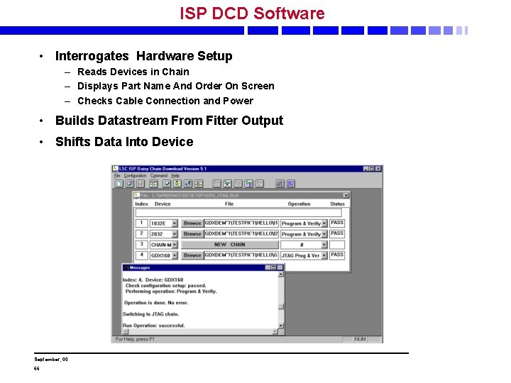
ISP DCD Software • Interrogates Hardware Setup – Reads Devices in Chain – Displays Part Name And Order On Screen – Checks Cable Connection and Power • Builds Datastream From Fitter Output • Shifts Data Into Device September, 00 66
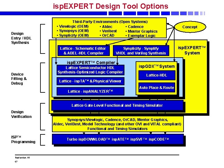
isp. EXPERT Design Tool Options Design Entry / HDL Synthesis Third-Party Environments (Open Systems) • Viewlogic (OEM) • Aldec • Cadence • Synopsys (OEM) • Veribest • Mentor Graphics • Synplicity (OEM) • Or. CAD • Exemplar Logic Lattice - Schematic Editor & ABEL-HDL Compiler Synplicity - Synplify VHDL and Verilog Synthesis isp. EXPERTTM Compiler Device Fitting & Debug Lattice Semiconductor HDL Synthesis-Optimized Logic Compiler Concept isp. EXPERTTM System isp. GDXTM System Lattice-HDL Lattice - isp. TATM & Physical Viewer Lattice - isp. ANALYZERTM Auto Place & Route Lattice Gate-Level Functional and Timing Simulator Design Verification ISPTM Programming September, 00 67 Synopsys/Viewlogic, Cadence, Or. CAD, Mentor Graphics, Aldec, Veri. Best, Model Technology (and other OVI and VITAL compliant) Functional and Timing Simulators Turbo isp. DOWNLOADTM isp. ATETM isp. SVFTM isp. CODETM
PLD Usage September, 00 68
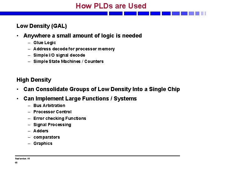
How PLDs are Used Low Density (GAL) • Anywhere a small amount of logic is needed – – Glue Logic Address decode for processor memory Simple I/O signal decode Simple State Machines / Counters High Density • Can Consolidate Groups of Low Density Into a Single Chip • Can Implement Large Functions / Systems – – – – September, 00 69 Bus Arbitration Processor Control Error checking Functions Signal Processing Adders comparators Graphics
Where PLDs are used PLDs Can Be Found in Most Major Electronics Industries • Datacom / Telecom – – – Switches Routers Hubs Modems CDMA/TDMA • Peripherals – Printers – Scanners – Fax Machines • Processing – Embedded processors / Single board computers • Industrial – Equipment Controllers • Data Acquisition September, 00 70
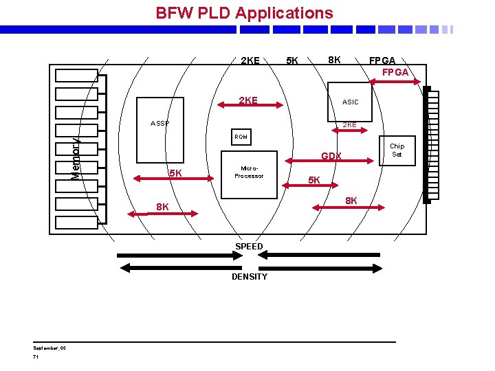
BFW PLD Applications 2 KE 8 K 5 K 2 KE ASIC ASSP 2 KE Memory ROM 5 K Micro. Processor 5 K 8 K SPEED DENSITY 71 Chip Set GDX 8 K September, 00 FPGA
BFW in Communications Equipment September, 00 72
- Slides: 72