Low power ASIC design CSEMCERN workshop 23 rd


- Slides: 35
Low power ASIC design CSEM/CERN workshop 23 rd May 2013
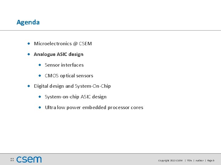
Agenda • Microelectronics @ CSEM • Analogue ASIC design • Sensor interfaces • CMOS optical sensors • Digital design and System-On-Chip • System-on-chip ASIC design • Ultra low power embedded processor cores Copyright 2013 CSEM | Title | Author | Page 1
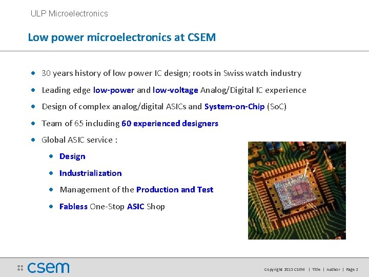
ULP Microelectronics Low power microelectronics at CSEM • 30 years history of low power IC design; roots in Swiss watch industry • Leading edge low-power and low-voltage Analog/Digital IC experience • Design of complex analog/digital ASICs and System-on-Chip (So. C) • Team of 65 including 60 experienced designers • Global ASIC service : • Design • Industrialization • Management of the Production and Test • Fabless One-Stop ASIC Shop Copyright 2013 CSEM | Title | Author | Page 2
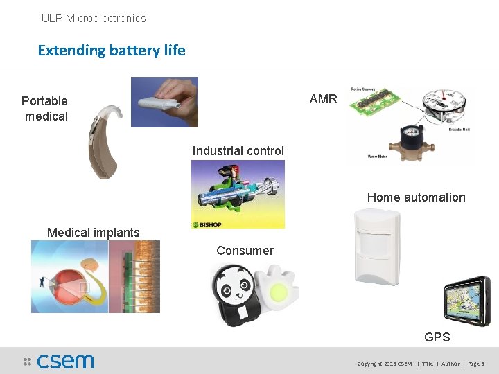
ULP Microelectronics Extending battery life AMR Portable medical Industrial control Home automation Medical implants Consumer GPS Copyright 2013 CSEM | Title | Author | Page 3
CSEM introduction Broad customer base Copyright 2013 CSEM | Title | Author | Page 4
Agenda • Microelectronics @ CSEM • Analogue ASIC design • Sensor interfaces • CMOS optical sensors • Digital design and System-On-Chip • System-on-chip ASIC design • Ultra low power embedded processor cores Copyright 2013 CSEM | Title | Author | Page 5
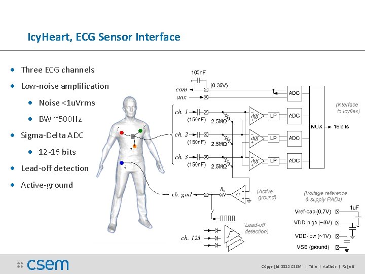
Icy. Heart, ECG Sensor Interface • Three ECG channels • Low-noise amplification • Noise <1 u. Vrms • BW ~500 Hz • Sigma-Delta ADC • 12 -16 bits • Lead-off detection • Active-ground Copyright 2013 CSEM | Title | Author | Page 6
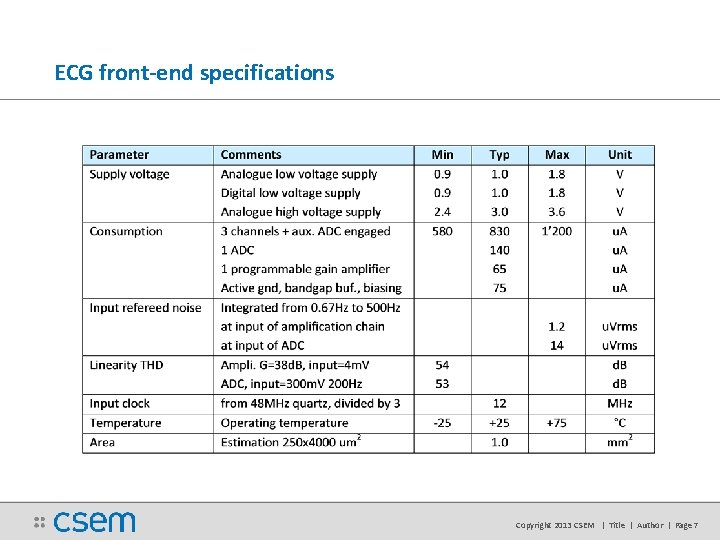
ECG front-end specifications Copyright 2013 CSEM | Title | Author | Page 7
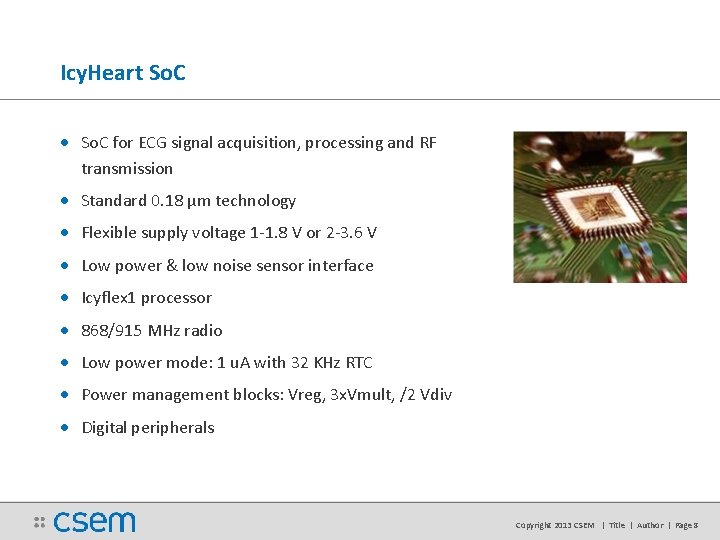
Icy. Heart So. C • So. C for ECG signal acquisition, processing and RF transmission • Standard 0. 18 μm technology • Flexible supply voltage 1 -1. 8 V or 2 -3. 6 V • Low power & low noise sensor interface • Icyflex 1 processor • 868/915 MHz radio • Low power mode: 1 u. A with 32 KHz RTC • Power management blocks: Vreg, 3 x. Vmult, /2 Vdiv • Digital peripherals Copyright 2013 CSEM | Title | Author | Page 8
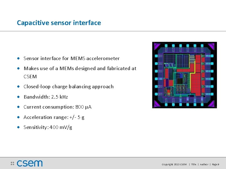
Capacitive sensor interface • Sensor interface for MEMS accelerometer • Makes use of a MEMs designed and fabricated at CSEM • Closed-loop charge balancing approach • Bandwidth: 2. 5 k. Hz • Current consumption: 800 µA • Acceleration range: +/- 5 g • Sensitivity: 400 m. V/g Copyright 2013 CSEM | Title | Author | Page 9
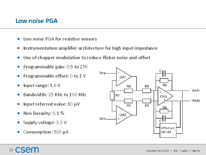
Low noise PGA • Low noise PGA for resistive sensors • Instrumentation amplifier architecture for high input impedance • Use of chopper modulation to reduce flicker noise and offset • Programmable gain: 0. 5 to 256 • Programmable offset: 0 to 1 V • Input range: 1. 6 V • Bandwidth: 25 KHz to 100 KHz • Input referred noise: 10 µV • Non linearity: 0. 1 % • Supply voltage: 3. 3 V • Consumption: 500 μA Copyright 2013 CSEM | Title | Author | Page 10
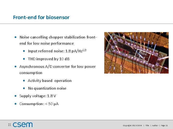
Front-end for biosensor • Noise cancelling chopper stabilization frontend for low noise performance • Input referred noise: 1. 8 p. A/Hz 1/2 • THD improved by 10 d. B • Asynchronous A/D converter for low power consumption • Activity based operation • No quantization noise • Supply voltage: 1. 8 V • Consumption: < 50 µA Copyright 2013 CSEM | Title | Author | Page 11
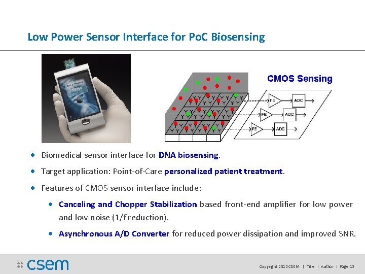
Low Power Sensor Interface for Po. C Biosensing CMOS Sensing • Biomedical sensor interface for DNA biosensing. • Target application: Point-of-Care personalized patient treatment. • Features of CMOS sensor interface include: • Canceling and Chopper Stabilization based front-end amplifier for low power and low noise (1/f reduction). • Asynchronous A/D Converter for reduced power dissipation and improved SNR. Copyright 2013 CSEM | Title | Author | Page 12
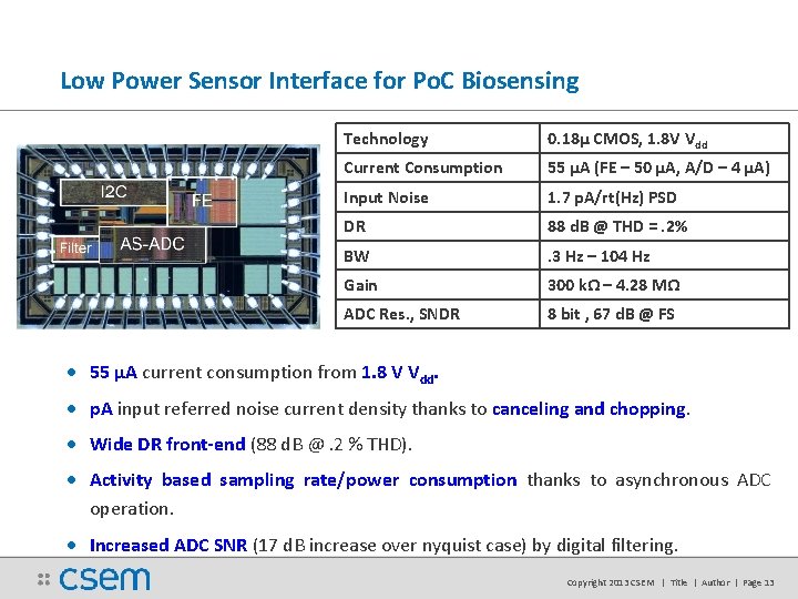
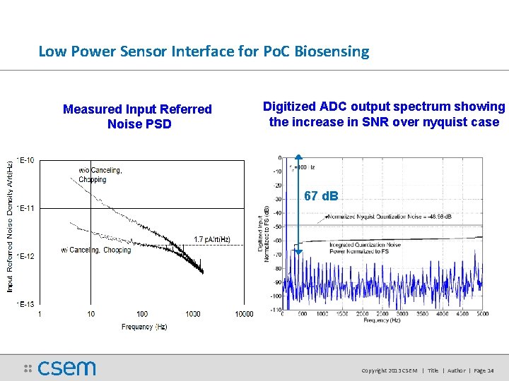
Low Power Sensor Interface for Po. C Biosensing Technology 0. 18µ CMOS, 1. 8 V Vdd Current Consumption 55 µA (FE – 50 µA, A/D – 4 µA) Input Noise 1. 7 p. A/rt(Hz) PSD DR 88 d. B @ THD =. 2% BW . 3 Hz – 104 Hz Gain 300 kΩ – 4. 28 MΩ ADC Res. , SNDR 8 bit , 67 d. B @ FS • 55 µA current consumption from 1. 8 V Vdd. • p. A input referred noise current density thanks to canceling and chopping. • Wide DR front-end (88 d. B @. 2 % THD). • Activity based sampling rate/power consumption thanks to asynchronous ADC operation. • Increased ADC SNR (17 d. B increase over nyquist case) by digital filtering. Copyright 2013 CSEM | Title | Author | Page 13
Low Power Sensor Interface for Po. C Biosensing Measured Input Referred Noise PSD Digitized ADC output spectrum showing the increase in SNR over nyquist case 67 d. B Copyright 2013 CSEM | Title | Author | Page 14
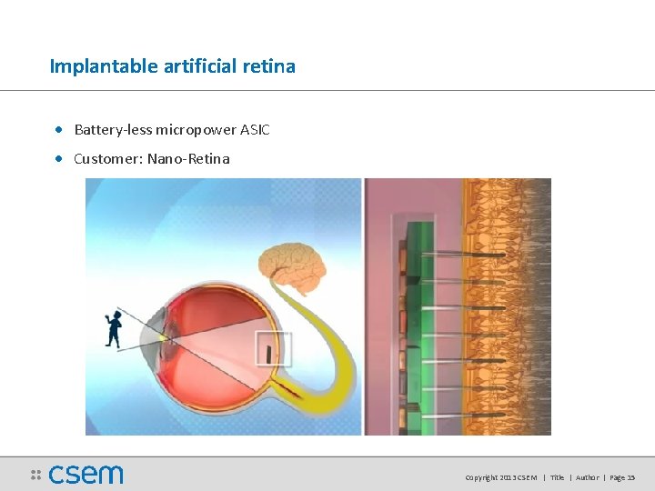
Implantable artificial retina • Battery-less micropower ASIC • Customer: Nano-Retina Copyright 2013 CSEM | Title | Author | Page 15
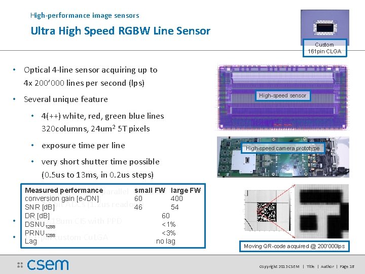
High-performance image sensors Ultra High Speed RGBW Line Sensor Custom 161 pin CLGA • Optical 4 -line sensor acquiring up to 4 x 200’ 000 lines per second (lps) • Several unique feature High-speed sensor • 4(++) white, red, green blue lines 320 columns, 24 um 2 5 T pixels • exposure time per line High-speed camera prototype • very short shutter time possible (0. 5 us to 13 ms, in 0. 2 us steps) • • Measured performance smalland FW large FW • on-chip column parallel CDS conversion gain [e-/DN] 60 400 10 -bit ADCs (1. 2 us readout) SNR [d. B] 46 54 DR [d. B] 60 UMC 0. 18 um CIS with PPD DSNU 1288 <1% PRNU 1288 <3% 161 -pin custom Cu. LGA Lag no lag Moving QR-code acquired @ 200’ 000 lps Copyright 2013 CSEM | Title | Author | Page 16
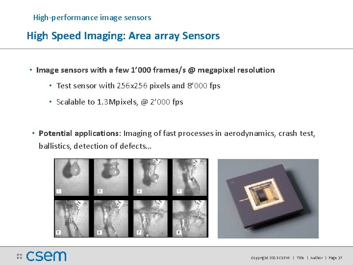
High-performance image sensors High Speed Imaging: Area array Sensors • Image sensors with a few 1’ 000 frames/s @ megapixel resolution • Test sensor with 256 x 256 pixels and 8’ 000 fps • Scalable to 1. 3 Mpixels, @ 2’ 000 fps • Potential applications: Imaging of fast processes in aerodynamics, crash test, ballistics, detection of defects… Copyright 2013 CSEM | Title | Author | Page 17
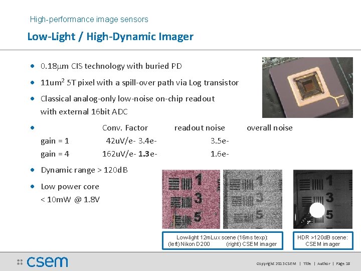
High-performance image sensors Low-Light / High-Dynamic Imager • 0. 18 mm CIS technology with buried PD • 11 um 2 5 T pixel with a spill-over path via Log transistor • Classical analog-only low-noise on-chip readout with external 16 bit ADC • gain = 1 gain = 4 Conv. Factor 42 u. V/e- 3. 4 e 162 u. V/e- 1. 3 e- readout noise 3. 5 e 1. 6 e- overall noise • Dynamic range > 120 d. B • Low power core < 10 m. W @ 1. 8 V Low-light 12 m. Lux scene (16 ms texp): (left) Nikon D 200 (right) CSEM imager HDR >120 d. B scene: CSEM imager Copyright 2013 CSEM | Title | Author | Page 18
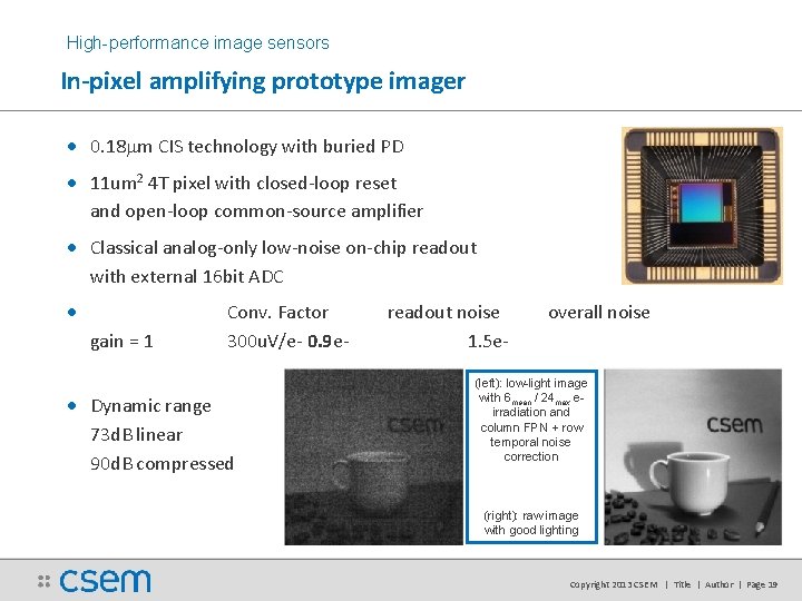
High-performance image sensors In-pixel amplifying prototype imager • 0. 18 mm CIS technology with buried PD • 11 um 2 4 T pixel with closed-loop reset and open-loop common-source amplifier • Classical analog-only low-noise on-chip readout with external 16 bit ADC • gain = 1 Conv. Factor 300 u. V/e- 0. 9 e- • Dynamic range 73 d. B linear 90 d. B compressed readout noise 1. 5 e- overall noise (left): low-light image with 6 mean / 24 max eirradiation and column FPN + row temporal noise correction (right): raw image with good lighting Copyright 2013 CSEM | Title | Author | Page 19
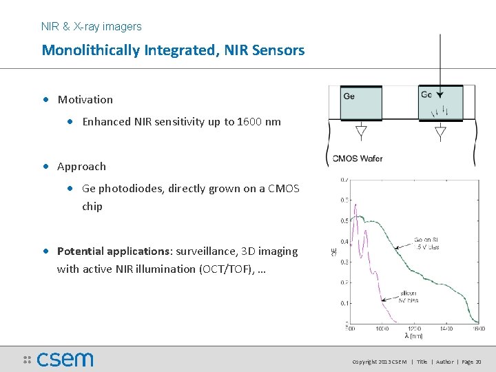
NIR & X-ray imagers Monolithically Integrated, NIR Sensors • Motivation • Enhanced NIR sensitivity up to 1600 nm • Approach • Ge photodiodes, directly grown on a CMOS chip • Potential applications: surveillance, 3 D imaging with active NIR illumination (OCT/TOF), … Copyright 2013 CSEM | Title | Author | Page 20
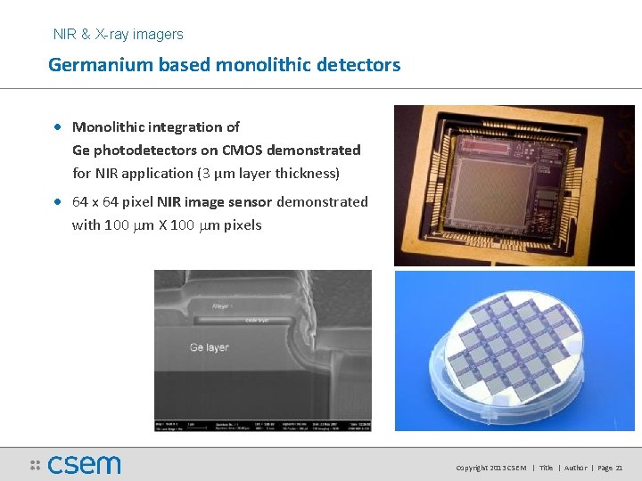
NIR & X-ray imagers Germanium based monolithic detectors • Monolithic integration of Ge photodetectors on CMOS demonstrated for NIR application (3 µm layer thickness) • 64 x 64 pixel NIR image sensor demonstrated with 100 mm X 100 mm pixels Copyright 2013 CSEM | Title | Author | Page 21
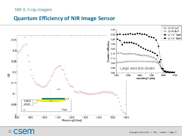
NIR & X-ray imagers Quantum Efficiency of NIR Image Sensor Large area test diodes Copyright 2013 CSEM | Title | Author | Page 22
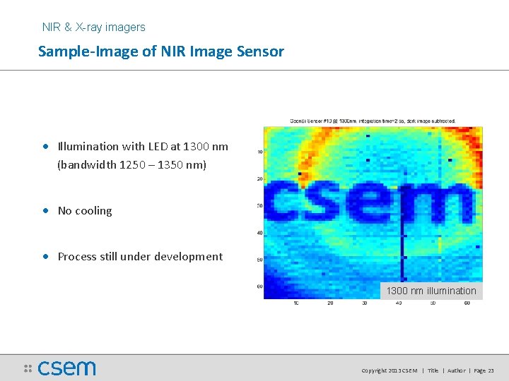
NIR & X-ray imagers Sample-Image of NIR Image Sensor • Illumination with LED at 1300 nm (bandwidth 1250 – 1350 nm) • No cooling • Process still under development 1300 nm illumination Copyright 2013 CSEM | Title | Author | Page 23
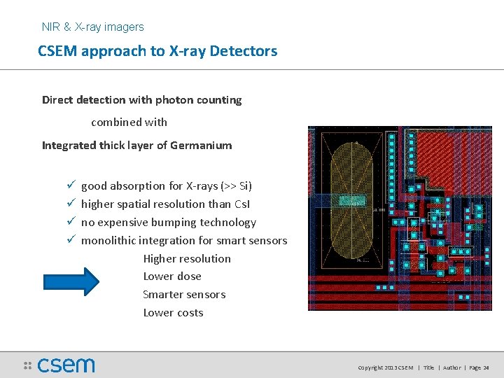
NIR & X-ray imagers CSEM approach to X-ray Detectors Direct detection with photon counting combined with Integrated thick layer of Germanium ü ü good absorption for X-rays (>> Si) higher spatial resolution than Cs. I no expensive bumping technology monolithic integration for smart sensors Higher resolution Lower dose Smarter sensors Lower costs Copyright 2013 CSEM | Title | Author | Page 24
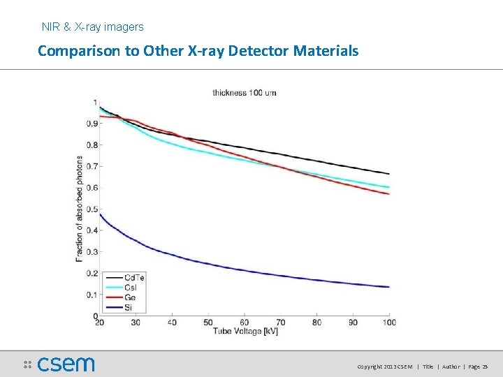
NIR & X-ray imagers Comparison to Other X-ray Detector Materials Copyright 2013 CSEM | Title | Author | Page 25
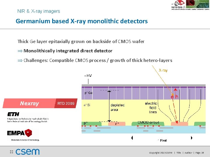
NIR & X-ray imagers Germanium based X-ray monolithic detectors Thick Ge layer epitaxially grown on backside of CMOS wafer Þ Monolithically integrated direct detector Þ Challenges: Compatible CMOS process / growth of thick hetero-layers Copyright 2013 CSEM | Title | Author | Page 26
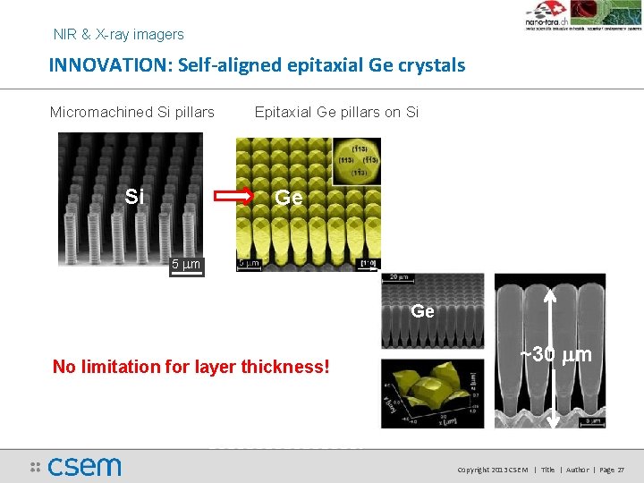
NIR & X-ray imagers INNOVATION: Self-aligned epitaxial Ge crystals Micromachined Si pillars Si Epitaxial Ge pillars on Si Ge 5 mm Ge No limitation for layer thickness! ~30 mm Copyright 2013 CSEM | Title | Author | Page 27
Agenda • Microelectronics @ CSEM • Analogue ASIC design • Sensor interfaces • CMOS optical sensors • Digital design and System-On-Chip • System-on-chip ASIC design • Ultra low power embedded processor cores Copyright 2013 CSEM | Title | Author | Page 28
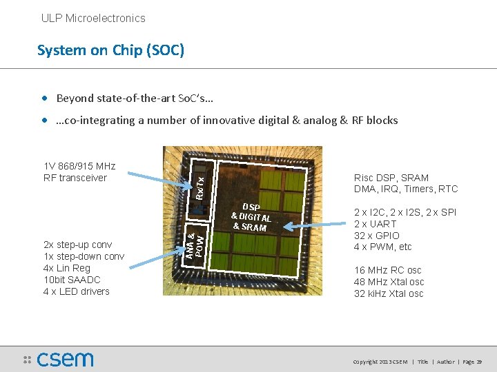
ULP Microelectronics System on Chip (SOC) • Beyond state-of-the-art So. C’s… • …co-integrating a number of innovative digital & analog & RF blocks Risc DSP, SRAM DMA, IRQ, Timers, RTC Rx/Tx 1 V 868/915 MHz RF transceiver 2 x step-up conv 1 x step-down conv 4 x Lin Reg 10 bit SAADC 4 x LED drivers ANA & POW DSP & DIGITAL & SRAM 2 x I 2 C, 2 x I 2 S, 2 x SPI 2 x UART 32 x GPIO 4 x PWM, etc 16 MHz RC osc 48 MHz Xtal osc 32 ki. Hz Xtal osc Copyright 2013 CSEM | Title | Author | Page 29
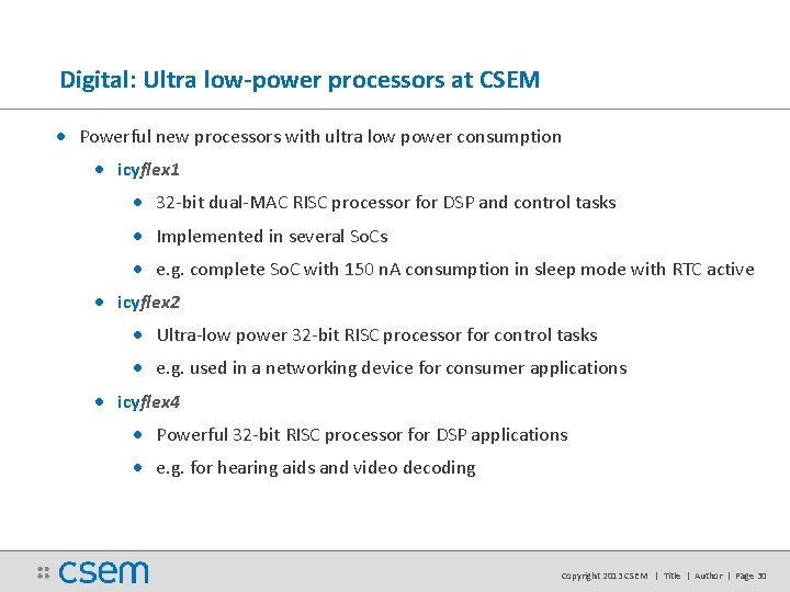
Digital: Ultra low-power processors at CSEM • Powerful new processors with ultra low power consumption • icyflex 1 • 32 -bit dual-MAC RISC processor for DSP and control tasks • Implemented in several So. Cs • e. g. complete So. C with 150 n. A consumption in sleep mode with RTC active • icyflex 2 • Ultra-low power 32 -bit RISC processor for control tasks • e. g. used in a networking device for consumer applications • icyflex 4 • Powerful 32 -bit RISC processor for DSP applications • e. g. for hearing aids and video decoding Copyright 2013 CSEM | Title | Author | Page 30
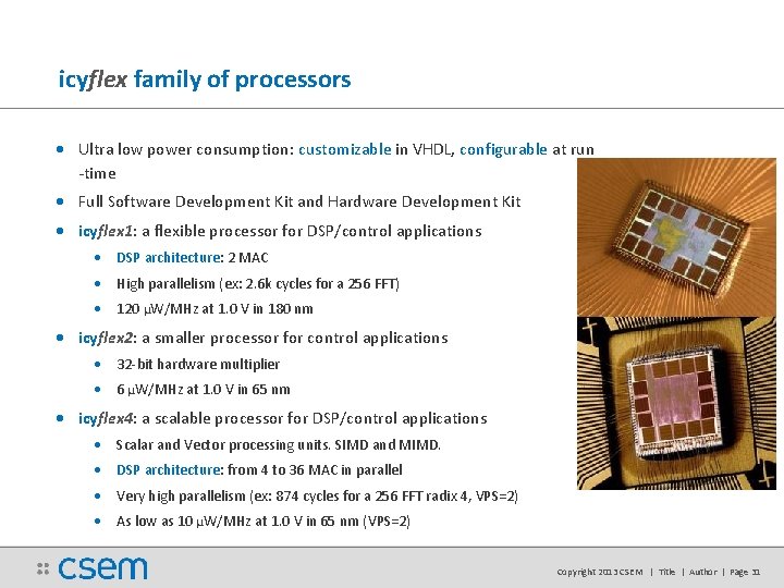
icyflex family of processors • Ultra low power consumption: customizable in VHDL, configurable at run -time • Full Software Development Kit and Hardware Development Kit • icyflex 1: a flexible processor for DSP/control applications • DSP architecture: 2 MAC • High parallelism (ex: 2. 6 k cycles for a 256 FFT) • 120 µW/MHz at 1. 0 V in 180 nm • icyflex 2: a smaller processor for control applications • 32 -bit hardware multiplier • 6 µW/MHz at 1. 0 V in 65 nm • icyflex 4: a scalable processor for DSP/control applications • Scalar and Vector processing units. SIMD and MIMD. • DSP architecture: from 4 to 36 MAC in parallel • Very high parallelism (ex: 874 cycles for a 256 FFT radix 4, VPS=2) • As low as 10 µW/MHz at 1. 0 V in 65 nm (VPS=2) Copyright 2013 CSEM | Title | Author | Page 31
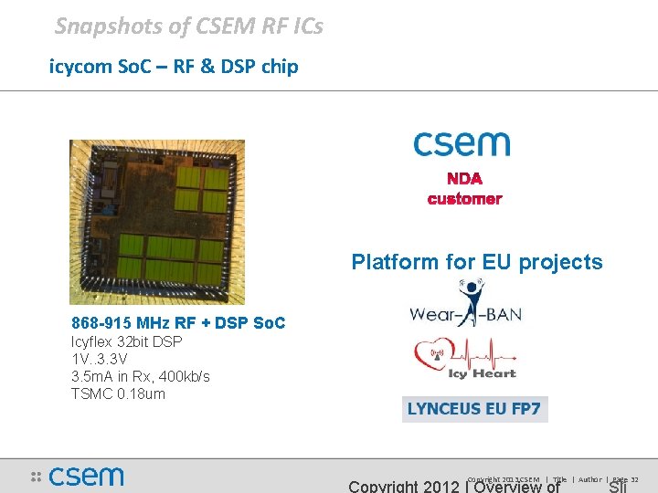
Snapshots of CSEM RF ICs icycom So. C – RF & DSP chip Platform for EU projects 868 -915 MHz RF + DSP So. C Icyflex 32 bit DSP 1 V. . 3. 3 V 3. 5 m. A in Rx, 400 kb/s TSMC 0. 18 um Copyright 2013 CSEM | Title | Author | Page 32
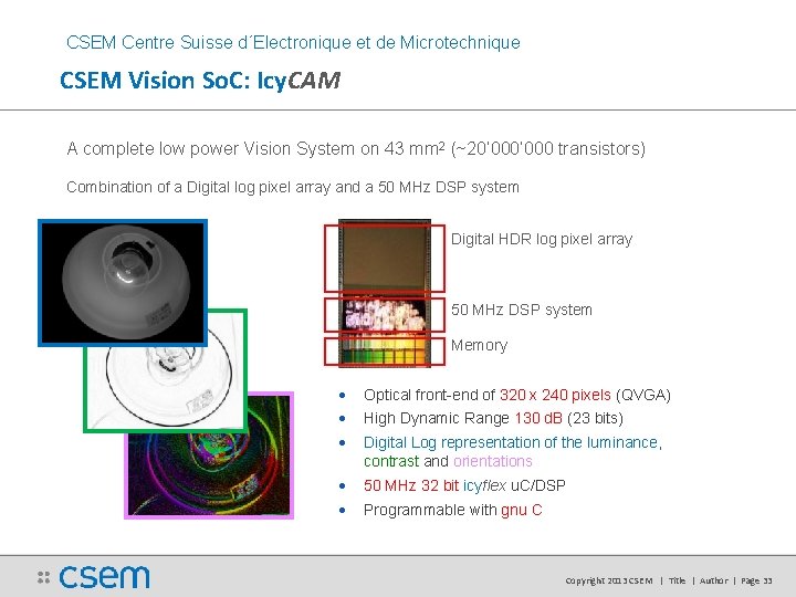
CSEM Centre Suisse d´Electronique et de Microtechnique CSEM Vision So. C: Icy. CAM A complete low power Vision System on 43 mm 2 (~20’ 000 transistors) Combination of a Digital log pixel array and a 50 MHz DSP system Digital HDR log pixel array 50 MHz DSP system Memory • Optical front-end of 320 x 240 pixels (QVGA) • High Dynamic Range 130 d. B (23 bits) • Digital Log representation of the luminance, contrast and orientations • 50 MHz 32 bit icyflex u. C/DSP • Programmable with gnu C Copyright 2013 CSEM | Title | Author | Page 33
Thank you for your attention!