Connecting Computer Modules Connecting All the units must
- Slides: 112

Connecting Computer Modules

Connecting • All the units must be connected • Different type of connection for different type of unit —Memory —Input/Output —CPU

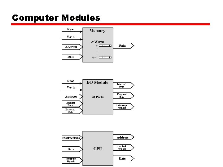
Computer Modules

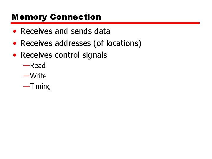
Memory Connection • Receives and sends data • Receives addresses (of locations) • Receives control signals —Read —Write —Timing

Input/Output Connection(1) • Similar to memory from computer’s viewpoint • Output —Receive data from computer —Send data to peripheral • Input —Receive data from peripheral —Send data to computer

Input/Output Connection(2) • Receive control signals from computer • Send control signals to peripherals —e. g. spin disk • Receive addresses from computer —e. g. port number to identify peripheral • Send interrupt signals (control)

CPU Connection • • Reads instruction and data Writes out data (after processing) Sends control signals to other units Receives (& acts on) interrupts

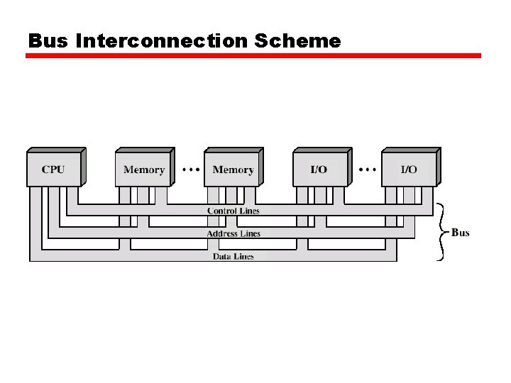
Buses • There a number of possible interconnection systems • Single and multiple BUS structures are most common • e. g. Control/Address/Data bus (PC) • e. g. Unibus (DEC-PDP)

What is a Bus? • A communication pathway connecting two or more devices • Usually broadcast • Often grouped —A number of channels in one bus —e. g. 32 bit data bus is 32 separate single bit channels • Power lines may not be shown

Data Bus • Carries data —Remember that there is no difference between “data” and “instruction” at this level • Width is a key determinant of performance — 8, 16, 32, 64 bit

Address bus • Identify the source or destination of data • e. g. CPU needs to read an instruction (data) from a given location in memory • Bus width determines maximum memory capacity of system —e. g. 8080 has 16 bit address bus giving 64 k address space

Control Bus • Control and timing information —Memory read/write signal —Interrupt request —Clock signals

Bus Interconnection Scheme

Big and Yellow? • What do buses look like? —Parallel lines on circuit boards —Ribbon cables —Strip connectors on mother boards – e. g. PCI —Sets of wires

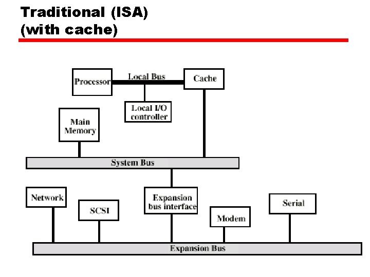
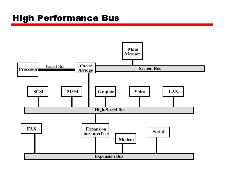
Single Bus Problems • Lots of devices on one bus leads to: —Propagation delays – Long data paths mean that co-ordination of bus use can adversely affect performance – If aggregate data transfer approaches bus capacity • Most systems use multiple buses to overcome these problems

Traditional (ISA) (with cache)

High Performance Bus

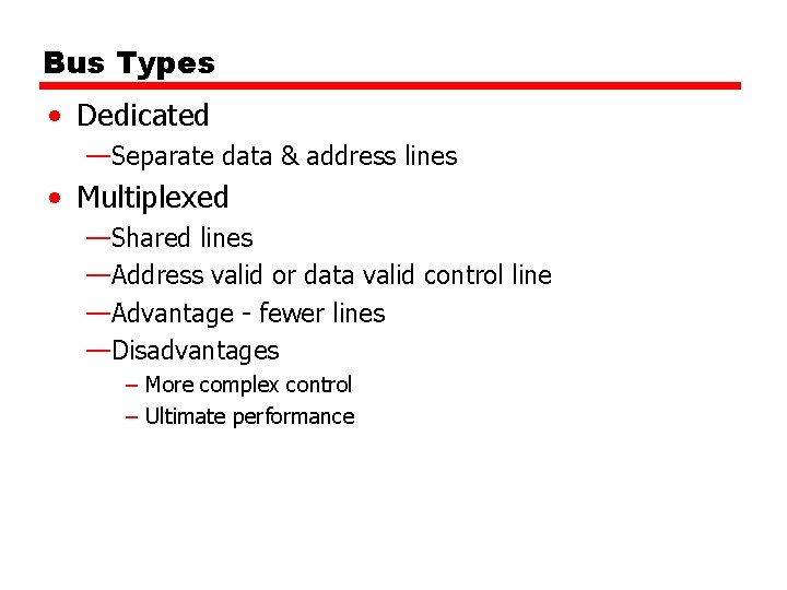
Bus Types • Dedicated —Separate data & address lines • Multiplexed —Shared lines —Address valid or data valid control line —Advantage - fewer lines —Disadvantages – More complex control – Ultimate performance

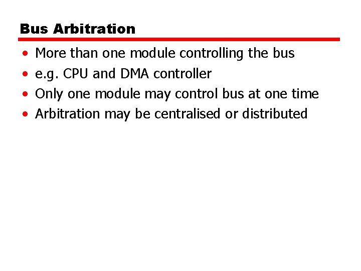
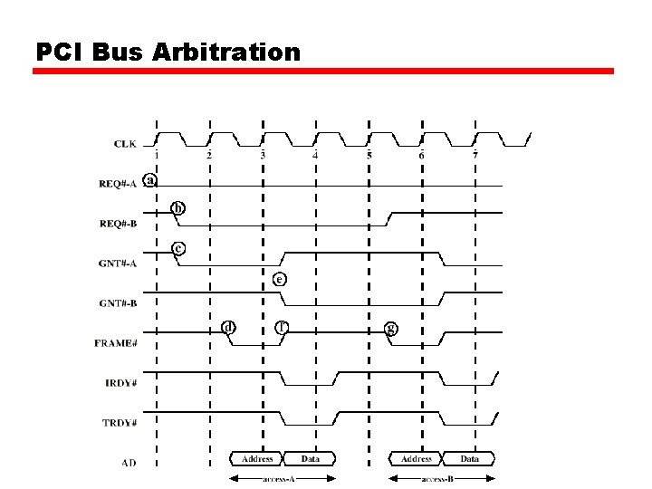
Bus Arbitration • • More than one module controlling the bus e. g. CPU and DMA controller Only one module may control bus at one time Arbitration may be centralised or distributed

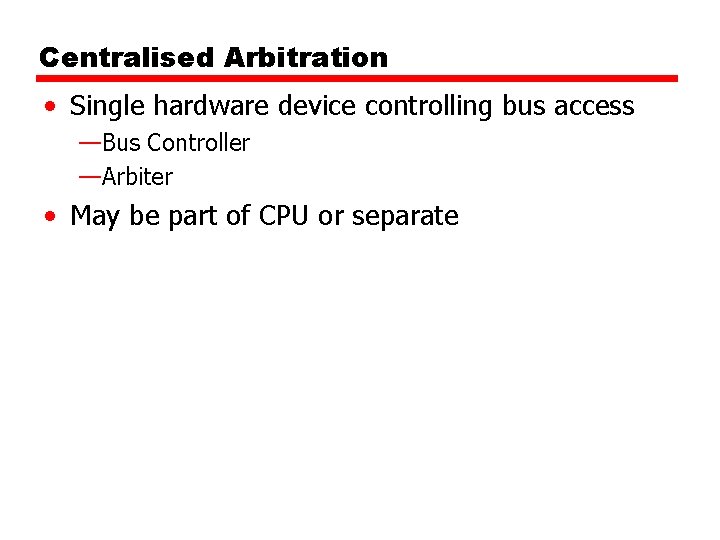
Centralised Arbitration • Single hardware device controlling bus access —Bus Controller —Arbiter • May be part of CPU or separate

Distributed Arbitration • Each module may claim the bus • Control logic on all modules

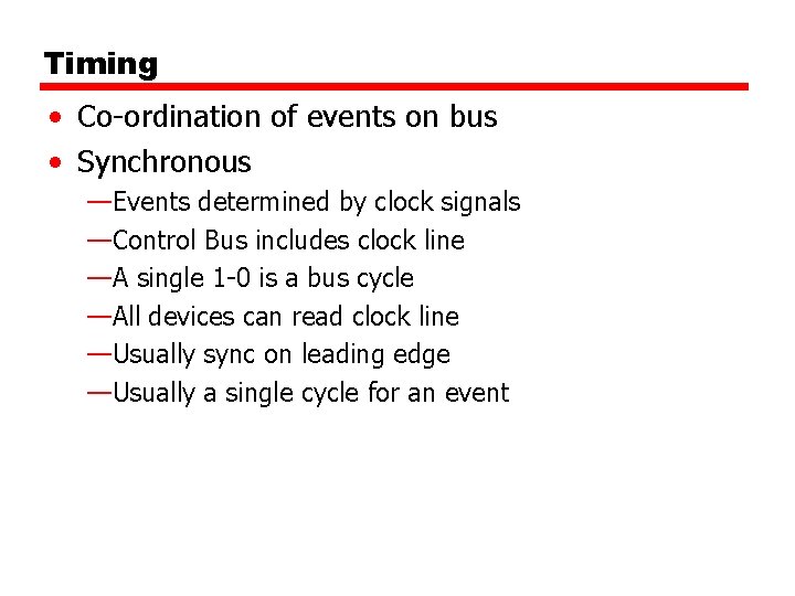
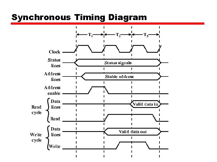
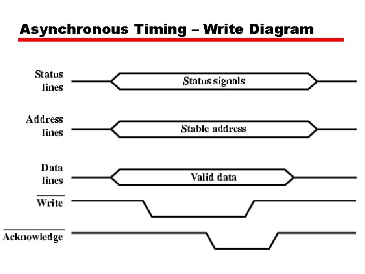
Timing • Co-ordination of events on bus • Synchronous —Events determined by clock signals —Control Bus includes clock line —A single 1 -0 is a bus cycle —All devices can read clock line —Usually sync on leading edge —Usually a single cycle for an event

Synchronous Timing Diagram

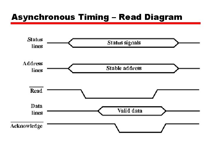
Asynchronous Timing – Read Diagram

Asynchronous Timing – Write Diagram

PCI Bus • • Peripheral Component Interconnection Intel released to public domain 32 or 64 bit 50 lines

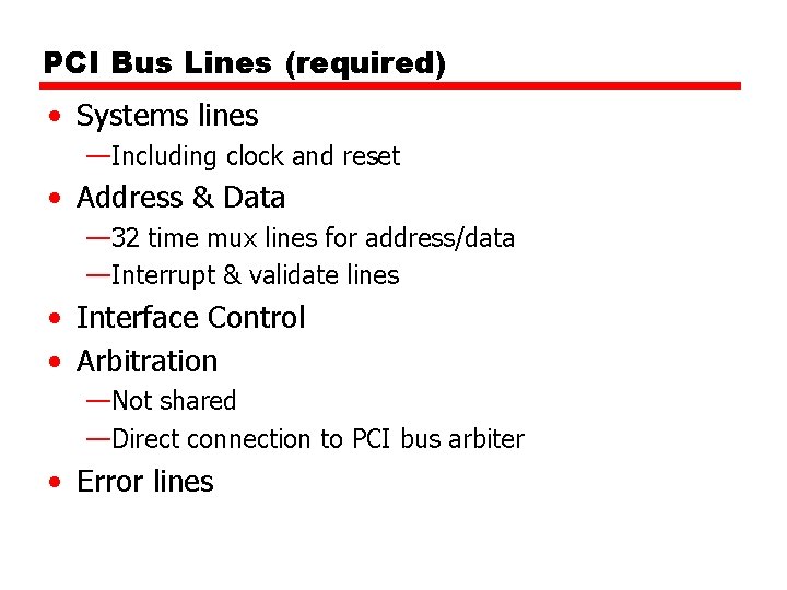
PCI Bus Lines (required) • Systems lines —Including clock and reset • Address & Data — 32 time mux lines for address/data —Interrupt & validate lines • Interface Control • Arbitration —Not shared —Direct connection to PCI bus arbiter • Error lines

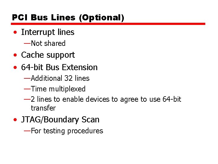
PCI Bus Lines (Optional) • Interrupt lines —Not shared • Cache support • 64 -bit Bus Extension —Additional 32 lines —Time multiplexed — 2 lines to enable devices to agree to use 64 -bit transfer • JTAG/Boundary Scan —For testing procedures

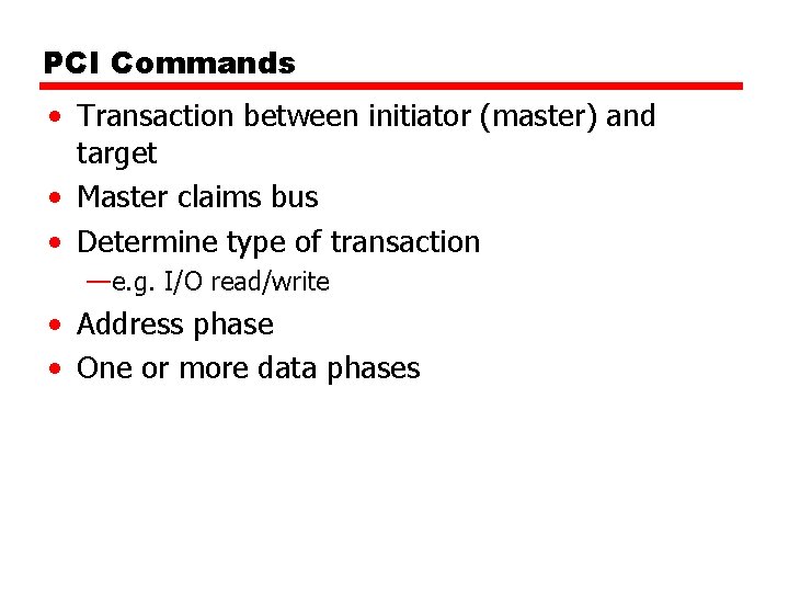
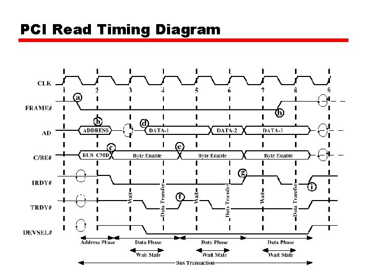
PCI Commands • Transaction between initiator (master) and target • Master claims bus • Determine type of transaction —e. g. I/O read/write • Address phase • One or more data phases

PCI Read Timing Diagram

PCI Bus Arbitration

Memory Structures • Mix chapter 4 and 5

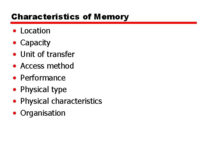
Characteristics of Memory • • Location Capacity Unit of transfer Access method Performance Physical type Physical characteristics Organisation

Location • CPU • Internal • External

Capacity • Word size —The natural unit of organization • Number of words —or Bytes

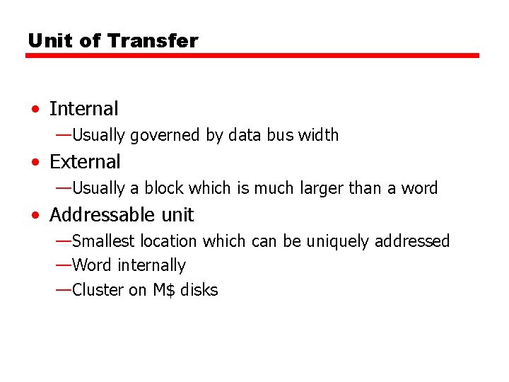
Unit of Transfer • Internal —Usually governed by data bus width • External —Usually a block which is much larger than a word • Addressable unit —Smallest location which can be uniquely addressed —Word internally —Cluster on M$ disks

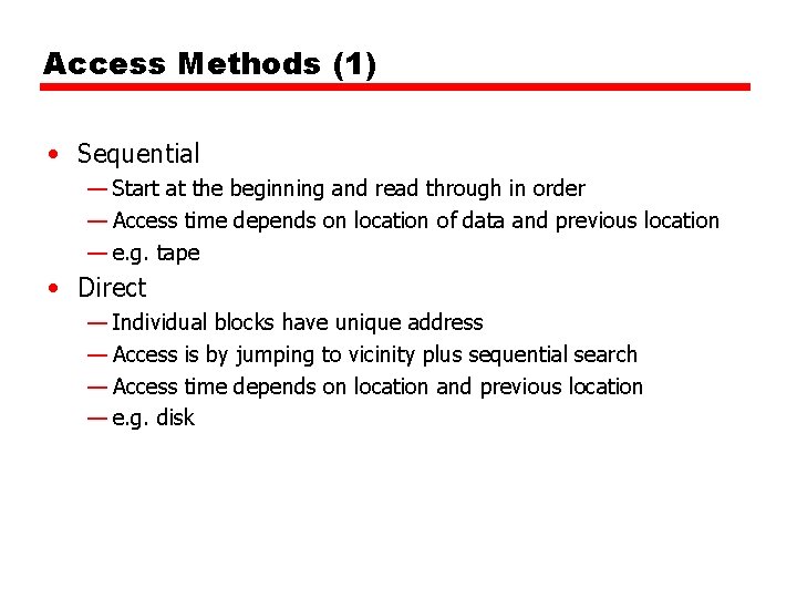
Access Methods (1) • Sequential — Start at the beginning and read through in order — Access time depends on location of data and previous location — e. g. tape • Direct — Individual blocks have unique address — Access is by jumping to vicinity plus sequential search — Access time depends on location and previous location — e. g. disk

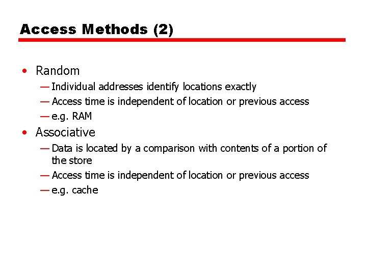
Access Methods (2) • Random — Individual addresses identify locations exactly — Access time is independent of location or previous access — e. g. RAM • Associative — Data is located by a comparison with contents of a portion of the store — Access time is independent of location or previous access — e. g. cache

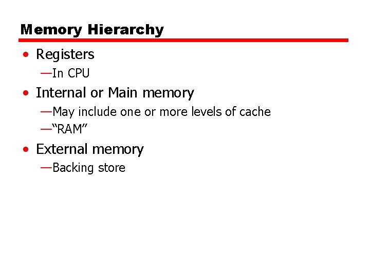
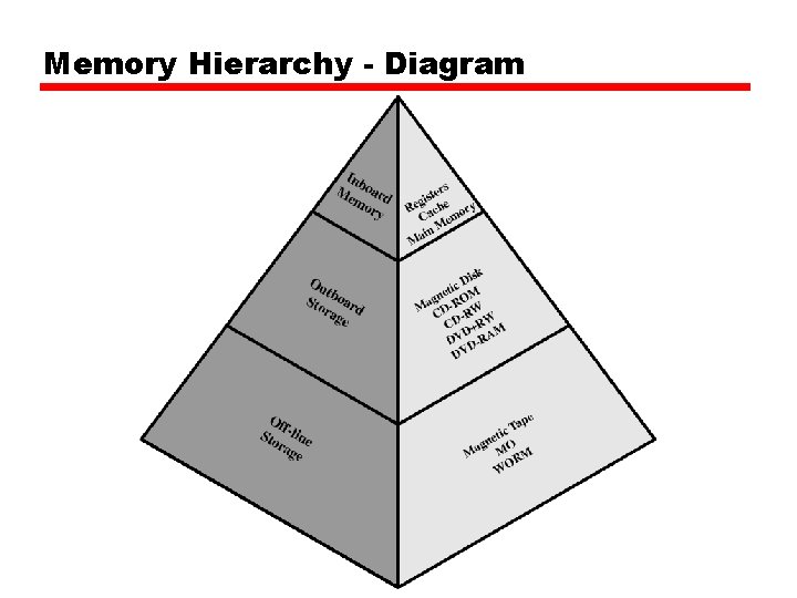
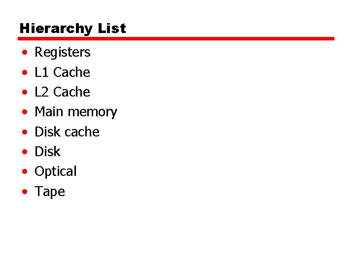
Memory Hierarchy • Registers —In CPU • Internal or Main memory —May include one or more levels of cache —“RAM” • External memory —Backing store

Memory Hierarchy - Diagram

Performance • Access time —Time between presenting the address and getting the valid data • Memory Cycle time —Time may be required for the memory to “recover” before next access —Cycle time is access + recovery • Transfer Rate —Rate at which data can be moved

Physical Types • Semiconductor —RAM • Magnetic —Disk & Tape • Optical —CD & DVD • Others —Bubble —Hologram

Physical Characteristics • • Decay Volatility Erasable Power consumption

Organization • Physical arrangement of bits into words • Not always obvious • e. g. interleaved

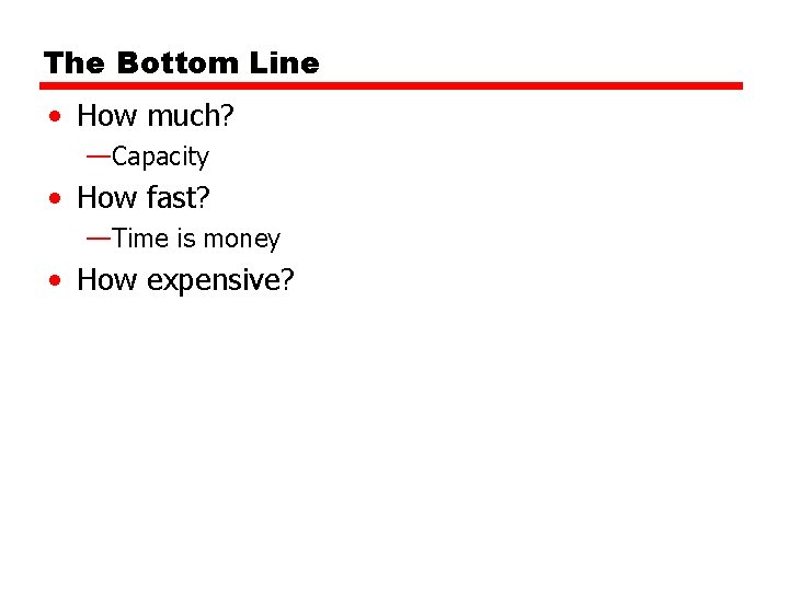
The Bottom Line • How much? —Capacity • How fast? —Time is money • How expensive?

Hierarchy List • • Registers L 1 Cache L 2 Cache Main memory Disk cache Disk Optical Tape

Internal Memory

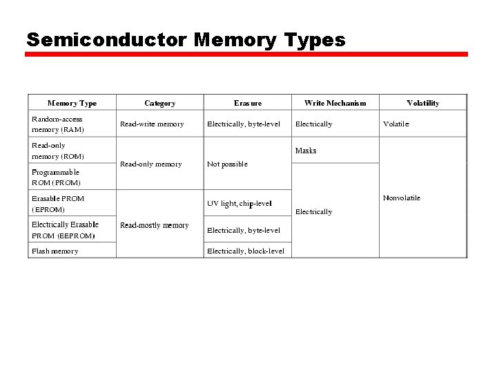
Semiconductor Memory Types

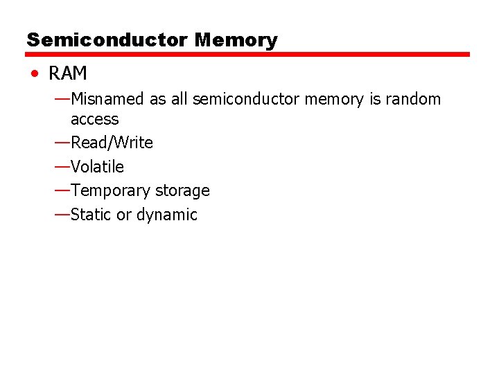
Semiconductor Memory • RAM —Misnamed as all semiconductor memory is random access —Read/Write —Volatile —Temporary storage —Static or dynamic

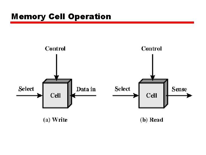
Memory Cell Operation

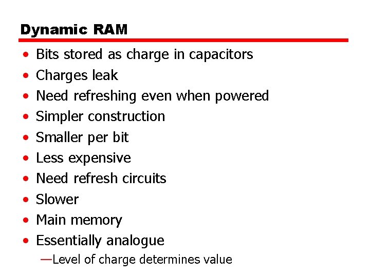
Dynamic RAM • • • Bits stored as charge in capacitors Charges leak Need refreshing even when powered Simpler construction Smaller per bit Less expensive Need refresh circuits Slower Main memory Essentially analogue —Level of charge determines value

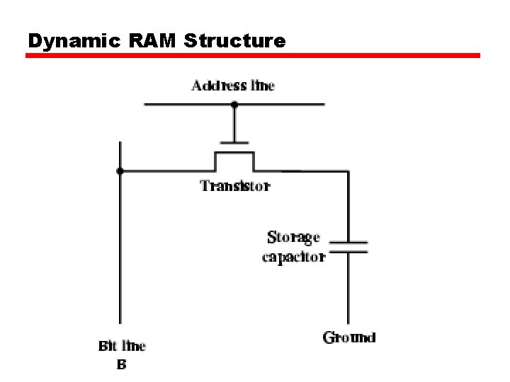
Dynamic RAM Structure

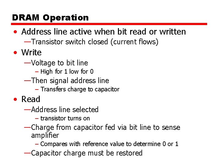
DRAM Operation • Address line active when bit read or written —Transistor switch closed (current flows) • Write —Voltage to bit line – High for 1 low for 0 —Then signal address line – Transfers charge to capacitor • Read —Address line selected – transistor turns on —Charge from capacitor fed via bit line to sense amplifier – Compares with reference value to determine 0 or 1 —Capacitor charge must be restored

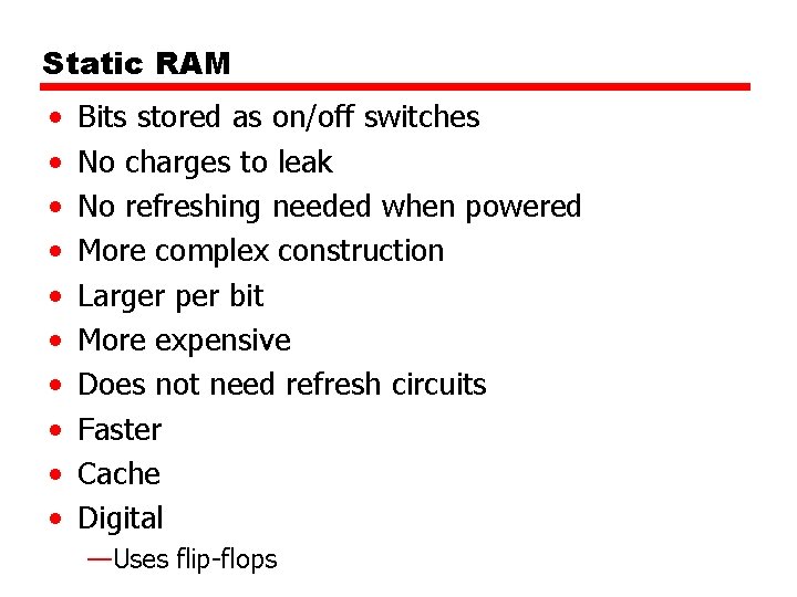
Static RAM • • • Bits stored as on/off switches No charges to leak No refreshing needed when powered More complex construction Larger per bit More expensive Does not need refresh circuits Faster Cache Digital —Uses flip-flops

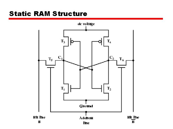
Static RAM Structure

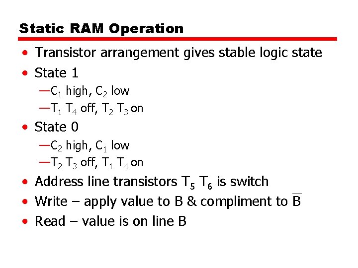
Static RAM Operation • Transistor arrangement gives stable logic state • State 1 —C 1 high, C 2 low —T 1 T 4 off, T 2 T 3 on • State 0 —C 2 high, C 1 low —T 2 T 3 off, T 1 T 4 on • Address line transistors T 5 T 6 is switch • Write – apply value to B & compliment to B • Read – value is on line B

SRAM v DRAM • Both volatile —Power needed to preserve data • Dynamic cell —Simpler to build, smaller —More dense —Less expensive —Needs refresh —Larger memory units • Static —Faster —Cache

Read Only Memory (ROM) • Permanent storage —Nonvolatile • • Microprogramming (see later) Library subroutines Systems programs (BIOS) Function tables

Types of ROM • Written during manufacture —Very expensive for small runs • Programmable (once) —PROM —Needs special equipment to program • Read “mostly” —Erasable Programmable (EPROM) – Erased by UV —Electrically Erasable (EEPROM) – Takes much longer to write than read —Flash memory – Erase whole memory electrically

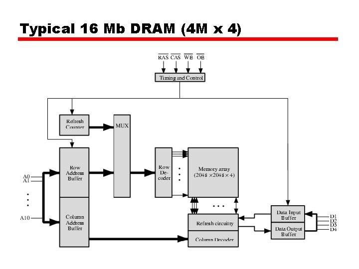
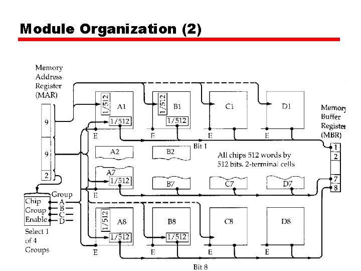
Organization in detail • A 16 Mbit chip can be organised as 1 M of 16 bit words • A bit per chip system has 16 lots of 1 Mbit chip with bit 1 of each word in chip 1 and so on • A 16 Mbit chip can be organised as a 2048 x 4 bit array —Reduces number of address pins – Multiplex row address and column address – 11 pins to address (211=2048) – Adding one more pin doubles range of values so x 4 capacity

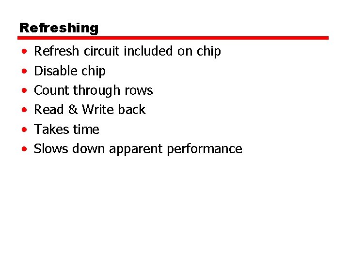
Refreshing • • • Refresh circuit included on chip Disable chip Count through rows Read & Write back Takes time Slows down apparent performance

Typical 16 Mb DRAM (4 M x 4)

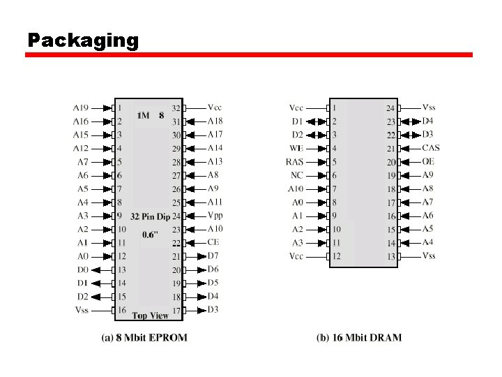
Packaging

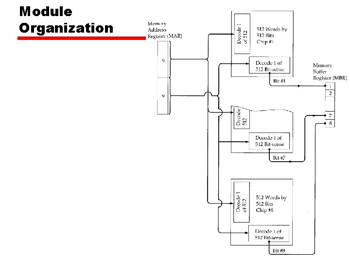
Module Organization

Module Organization (2)

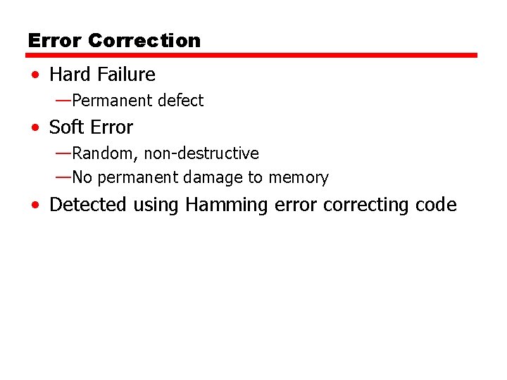
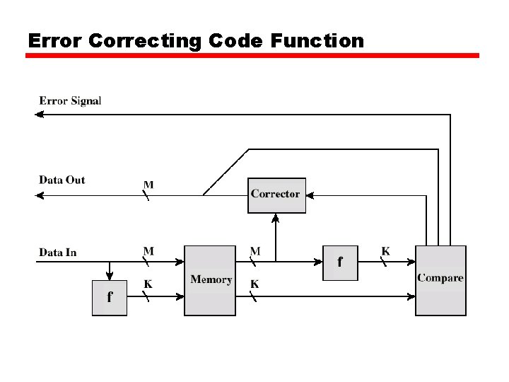
Error Correction • Hard Failure —Permanent defect • Soft Error —Random, non-destructive —No permanent damage to memory • Detected using Hamming error correcting code

Error Correcting Code Function

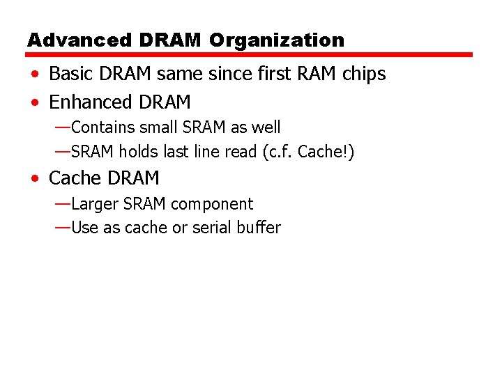
Advanced DRAM Organization • Basic DRAM same since first RAM chips • Enhanced DRAM —Contains small SRAM as well —SRAM holds last line read (c. f. Cache!) • Cache DRAM —Larger SRAM component —Use as cache or serial buffer

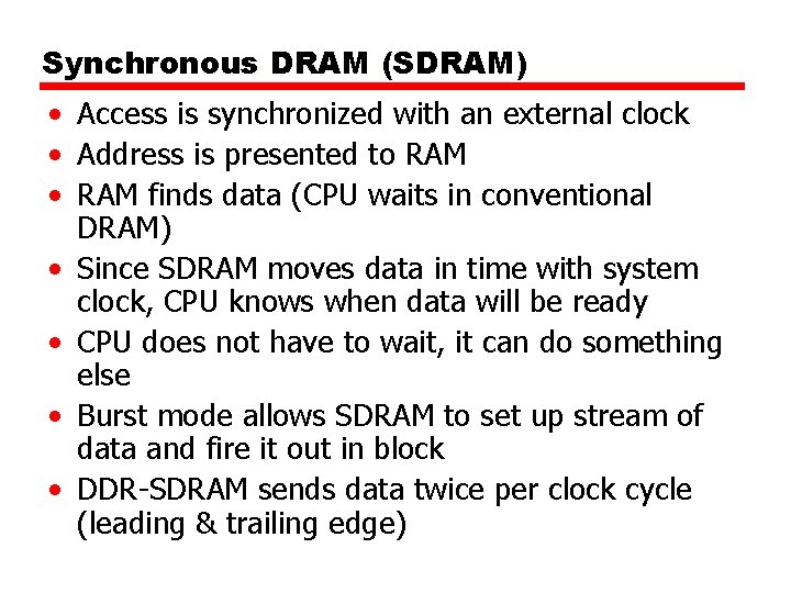
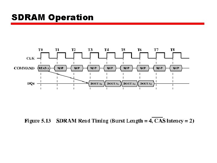
Synchronous DRAM (SDRAM) • Access is synchronized with an external clock • Address is presented to RAM • RAM finds data (CPU waits in conventional DRAM) • Since SDRAM moves data in time with system clock, CPU knows when data will be ready • CPU does not have to wait, it can do something else • Burst mode allows SDRAM to set up stream of data and fire it out in block • DDR-SDRAM sends data twice per clock cycle (leading & trailing edge)

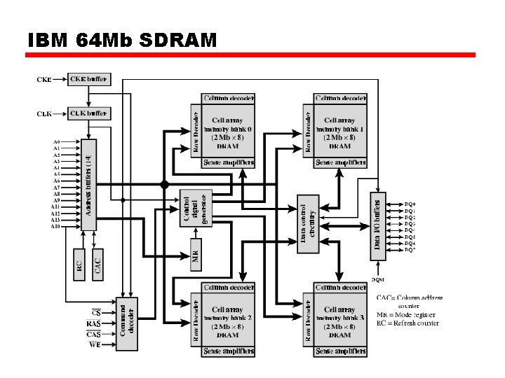
IBM 64 Mb SDRAM

SDRAM Operation

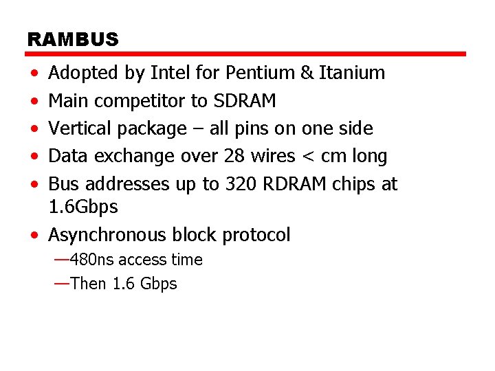
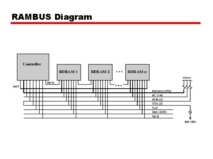
RAMBUS • • • Adopted by Intel for Pentium & Itanium Main competitor to SDRAM Vertical package – all pins on one side Data exchange over 28 wires < cm long Bus addresses up to 320 RDRAM chips at 1. 6 Gbps • Asynchronous block protocol — 480 ns access time —Then 1. 6 Gbps

RAMBUS Diagram

Cache Memory

So you want fast? • It is possible to build a computer which uses only static RAM (see later) • This would be very fast • This would need no cache —How can you cache? • This would cost a very large amount

Locality of Reference • During the course of the execution of a program, memory references tend to cluster • e. g. loops

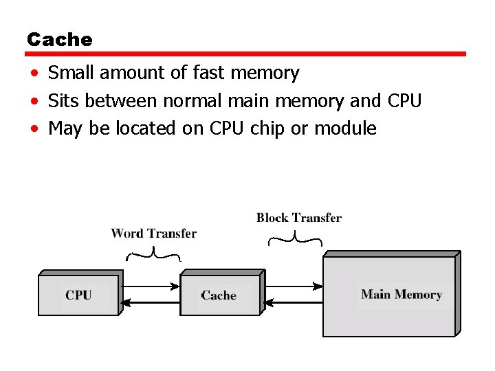
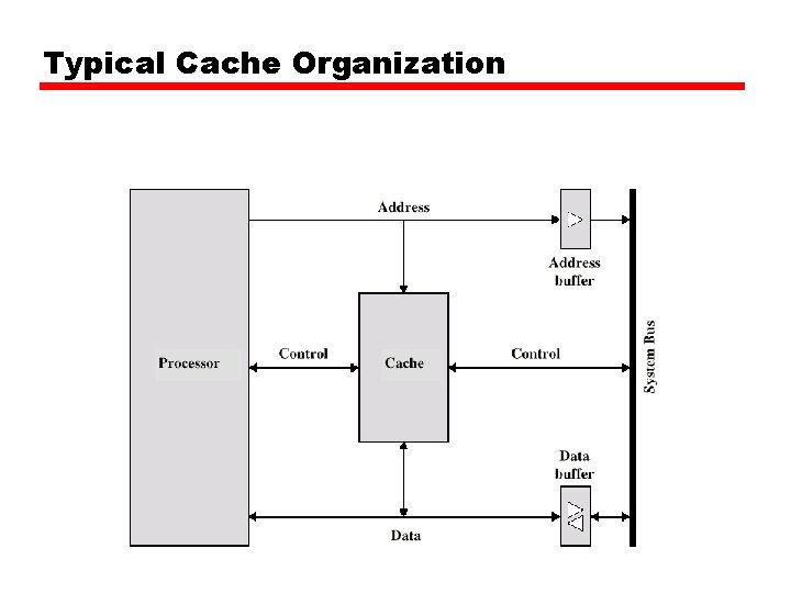
Cache • Small amount of fast memory • Sits between normal main memory and CPU • May be located on CPU chip or module

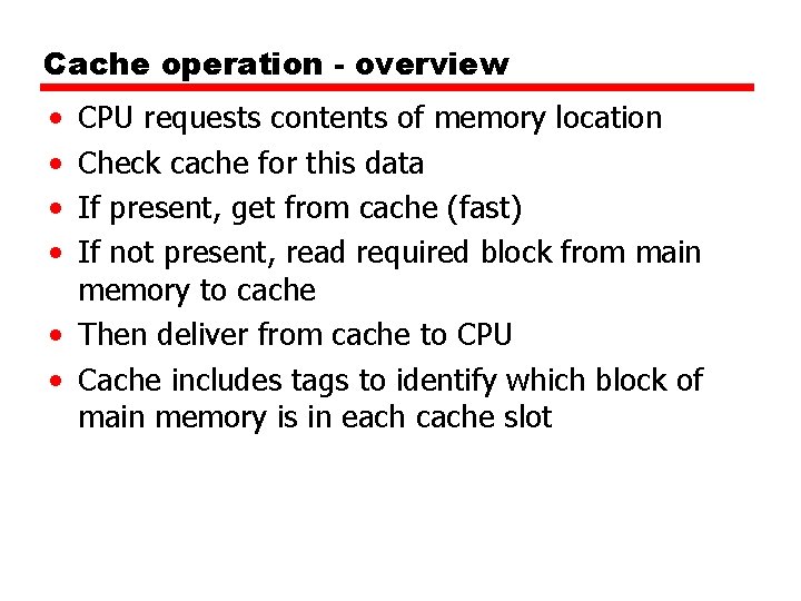
Cache operation - overview • • CPU requests contents of memory location Check cache for this data If present, get from cache (fast) If not present, read required block from main memory to cache • Then deliver from cache to CPU • Cache includes tags to identify which block of main memory is in each cache slot

Cache Design • • • Size Mapping Function Replacement Algorithm Write Policy Block Size Number of Caches

Size does matter • Cost —More cache is expensive • Speed —More cache is faster (up to a point) —Checking cache for data takes time

Typical Cache Organization

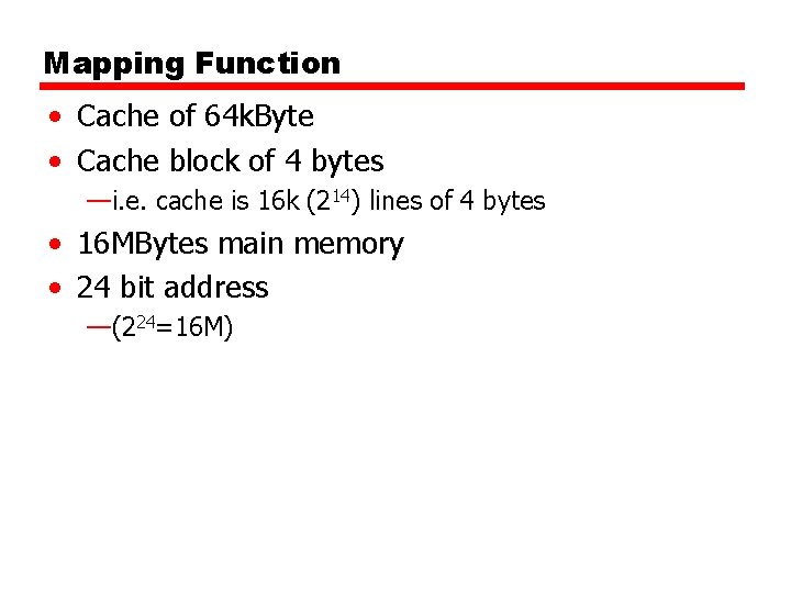
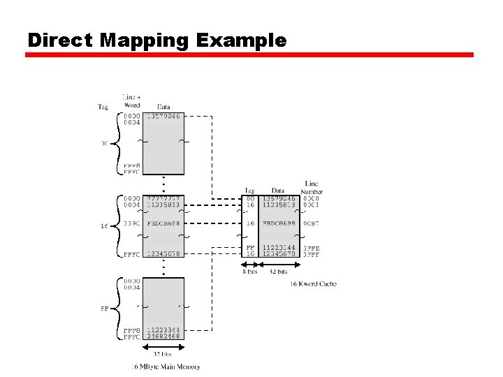
Mapping Function • Cache of 64 k. Byte • Cache block of 4 bytes —i. e. cache is 16 k (214) lines of 4 bytes • 16 MBytes main memory • 24 bit address —(224=16 M)

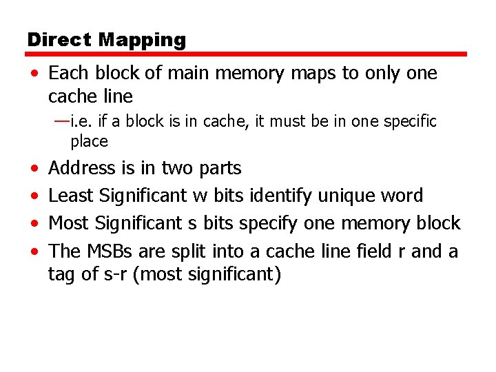
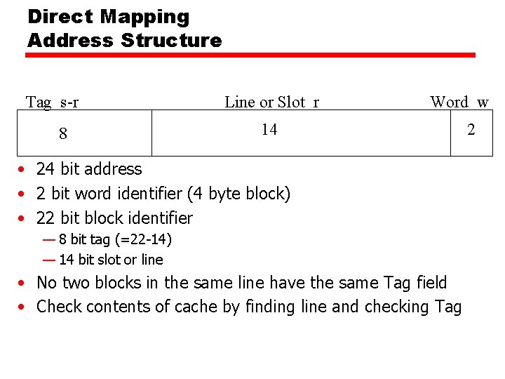
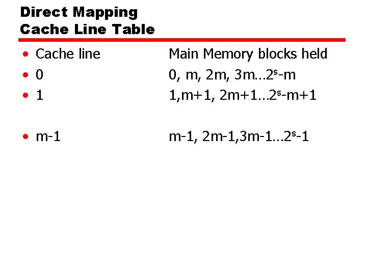
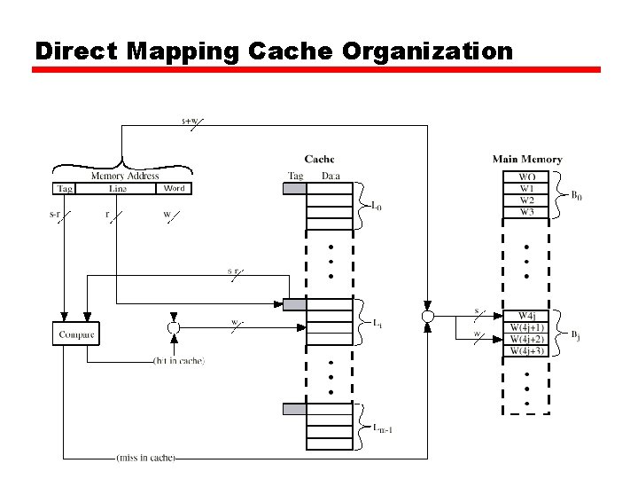
Direct Mapping • Each block of main memory maps to only one cache line —i. e. if a block is in cache, it must be in one specific place • • Address is in two parts Least Significant w bits identify unique word Most Significant s bits specify one memory block The MSBs are split into a cache line field r and a tag of s-r (most significant)

Direct Mapping Address Structure Tag s-r 8 Line or Slot r Word w 14 • 24 bit address • 2 bit word identifier (4 byte block) • 22 bit block identifier — 8 bit tag (=22 -14) — 14 bit slot or line • No two blocks in the same line have the same Tag field • Check contents of cache by finding line and checking Tag 2

Direct Mapping Cache Line Table • Cache line • 0 • 1 Main Memory blocks held 0, m, 2 m, 3 m… 2 s-m 1, m+1, 2 m+1… 2 s-m+1 • m-1, 2 m-1, 3 m-1… 2 s-1

Direct Mapping Cache Organization

Direct Mapping Example

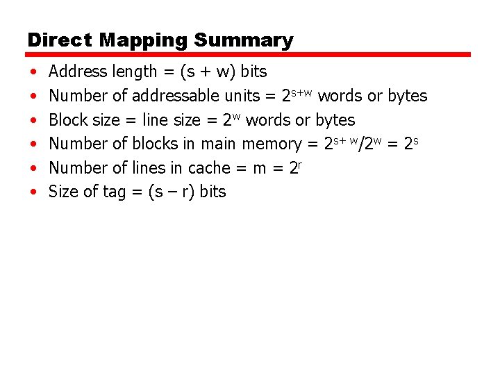
Direct Mapping Summary • • • Address length = (s + w) bits Number of addressable units = 2 s+w words or bytes Block size = line size = 2 w words or bytes Number of blocks in main memory = 2 s+ w/2 w = 2 s Number of lines in cache = m = 2 r Size of tag = (s – r) bits

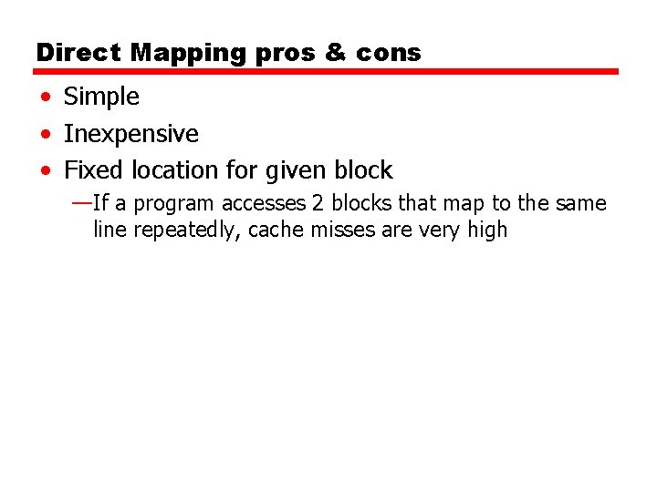
Direct Mapping pros & cons • Simple • Inexpensive • Fixed location for given block —If a program accesses 2 blocks that map to the same line repeatedly, cache misses are very high

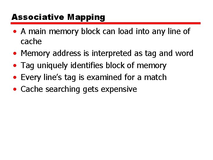
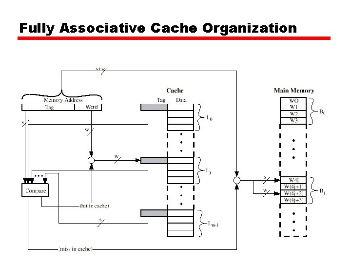
Associative Mapping • A main memory block can load into any line of cache • Memory address is interpreted as tag and word • Tag uniquely identifies block of memory • Every line’s tag is examined for a match • Cache searching gets expensive

Fully Associative Cache Organization

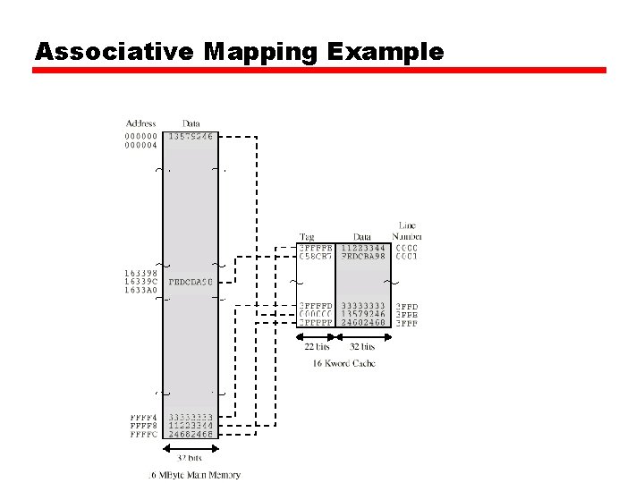
Associative Mapping Example

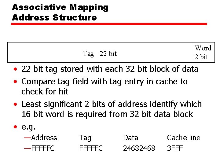
Associative Mapping Address Structure Word 2 bit Tag 22 bit • 22 bit tag stored with each 32 bit block of data • Compare tag field with tag entry in cache to check for hit • Least significant 2 bits of address identify which 16 bit word is required from 32 bit data block • e. g. —Address —FFFFFC Tag FFFFFC Data 2468 Cache line 3 FFF

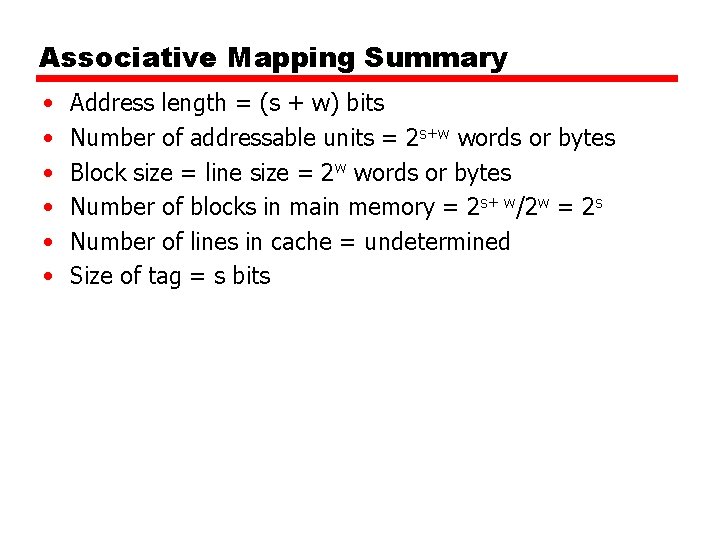
Associative Mapping Summary • • • Address length = (s + w) bits Number of addressable units = 2 s+w words or bytes Block size = line size = 2 w words or bytes Number of blocks in main memory = 2 s+ w/2 w = 2 s Number of lines in cache = undetermined Size of tag = s bits

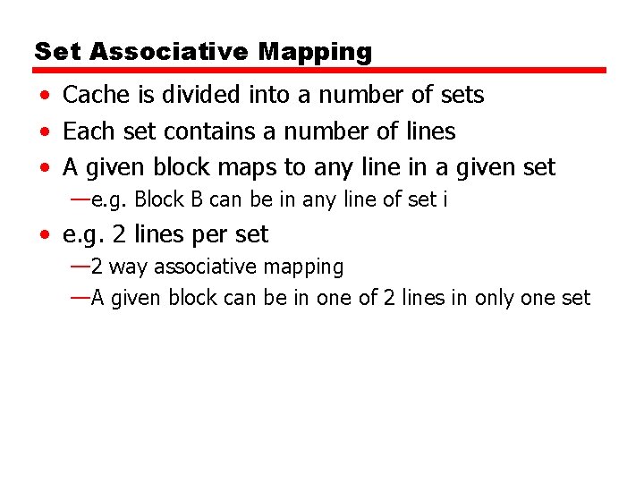
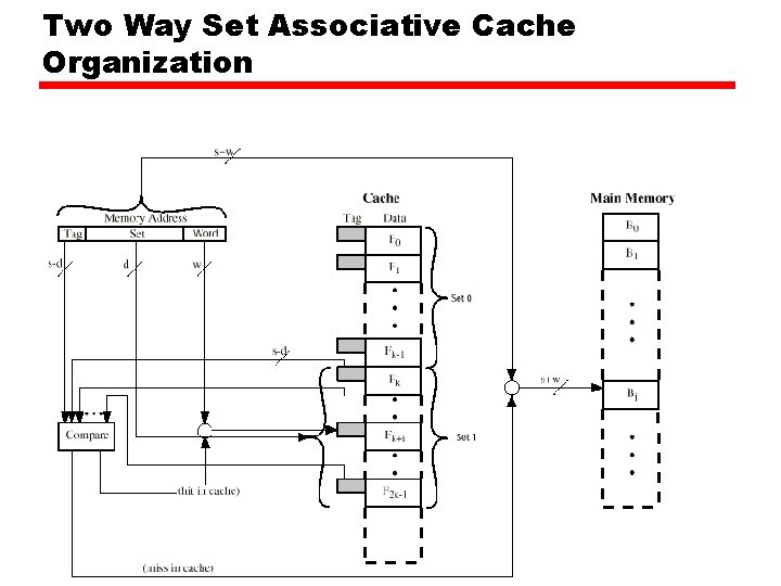
Set Associative Mapping • Cache is divided into a number of sets • Each set contains a number of lines • A given block maps to any line in a given set —e. g. Block B can be in any line of set i • e. g. 2 lines per set — 2 way associative mapping —A given block can be in one of 2 lines in only one set

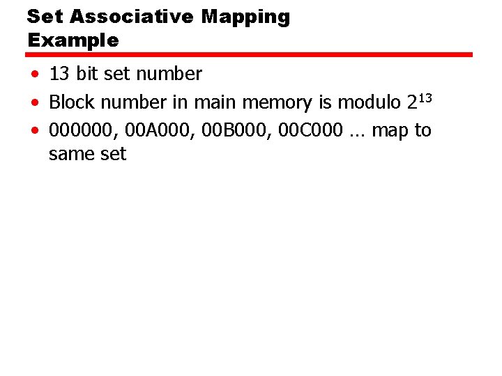
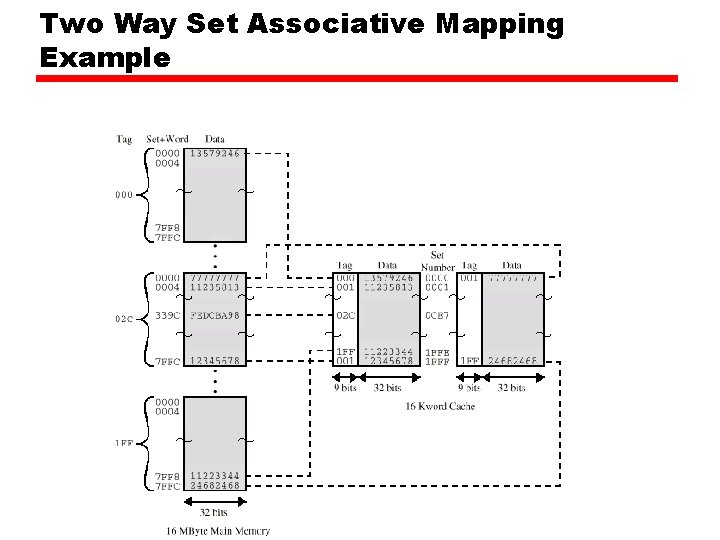
Set Associative Mapping Example • 13 bit set number • Block number in main memory is modulo 213 • 000000, 00 A 000, 00 B 000, 00 C 000 … map to same set

Two Way Set Associative Cache Organization

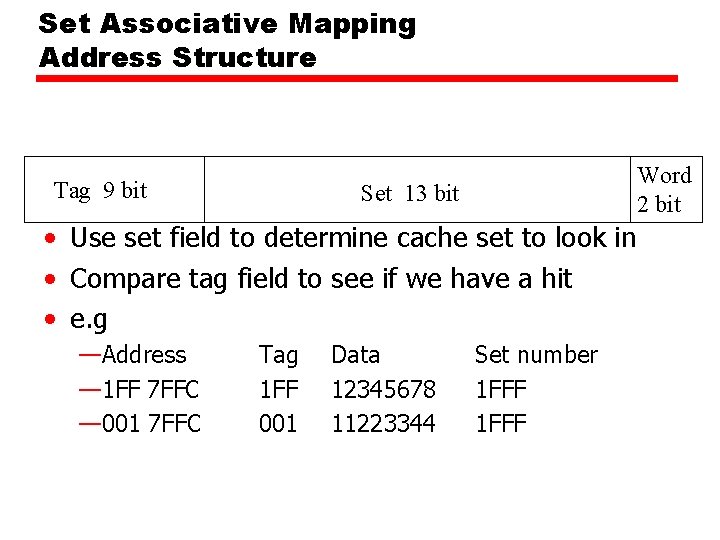
Set Associative Mapping Address Structure Tag 9 bit Word 2 bit Set 13 bit • Use set field to determine cache set to look in • Compare tag field to see if we have a hit • e. g —Address — 1 FF 7 FFC — 001 7 FFC Tag 1 FF 001 Data 12345678 11223344 Set number 1 FFF

Two Way Set Associative Mapping Example

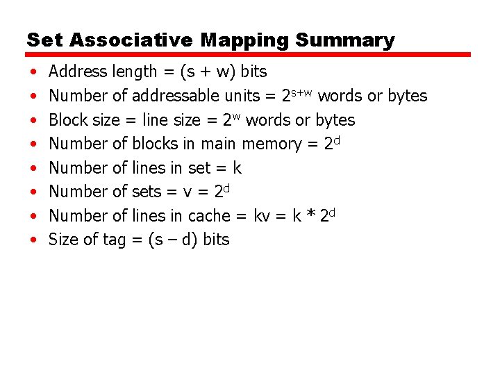
Set Associative Mapping Summary • • Address length = (s + w) bits Number of addressable units = 2 s+w words or bytes Block size = line size = 2 w words or bytes Number of blocks in main memory = 2 d Number of lines in set = k Number of sets = v = 2 d Number of lines in cache = kv = k * 2 d Size of tag = (s – d) bits

Replacement Algorithms (1) Direct mapping • No choice • Each block only maps to one line • Replace that line

Replacement Algorithms (2) Associative & Set Associative • Hardware implemented algorithm (speed) • Least Recently used (LRU) • e. g. in 2 way set associative —Which of the 2 block is lru? • First in first out (FIFO) —replace block that has been in cache longest • Least frequently used —replace block which has had fewest hits • Random

Write Policy • Must not overwrite a cache block unless main memory is up to date • Multiple CPUs may have individual caches • I/O may address main memory directly

Write through • All writes go to main memory as well as cache • Multiple CPUs can monitor main memory traffic to keep local (to CPU) cache up to date • Lots of traffic • Slows down writes • Remember bogus write through caches!

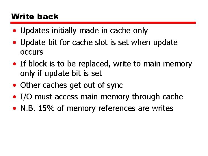
Write back • Updates initially made in cache only • Update bit for cache slot is set when update occurs • If block is to be replaced, write to main memory only if update bit is set • Other caches get out of sync • I/O must access main memory through cache • N. B. 15% of memory references are writes

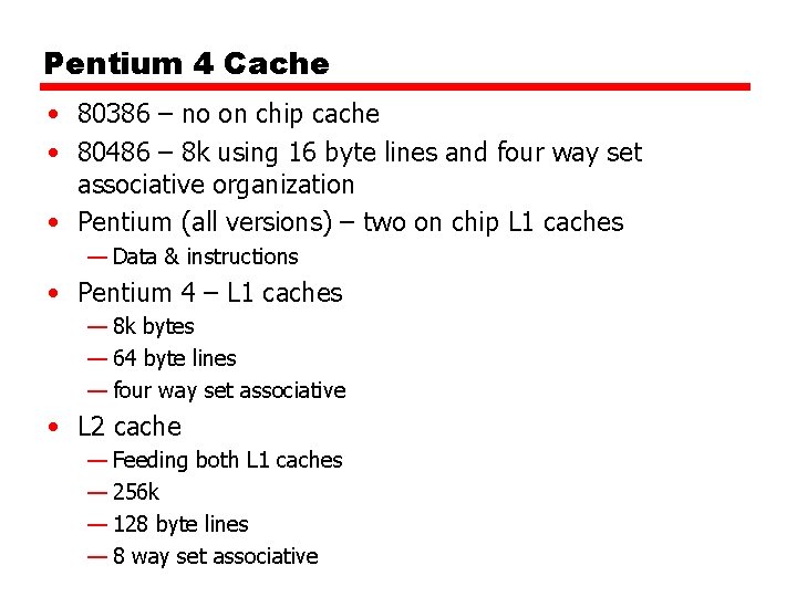
Pentium 4 Cache • 80386 – no on chip cache • 80486 – 8 k using 16 byte lines and four way set associative organization • Pentium (all versions) – two on chip L 1 caches — Data & instructions • Pentium 4 – L 1 caches — 8 k bytes — 64 byte lines — four way set associative • L 2 cache — Feeding both L 1 caches — 256 k — 128 byte lines — 8 way set associative

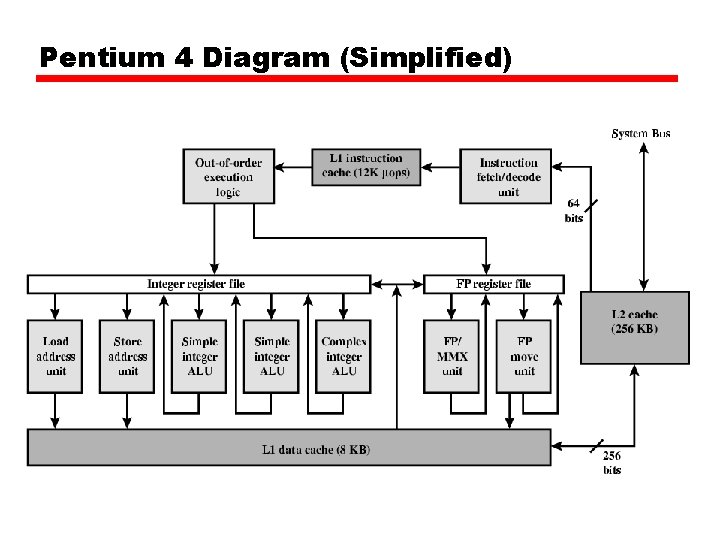
Pentium 4 Diagram (Simplified)

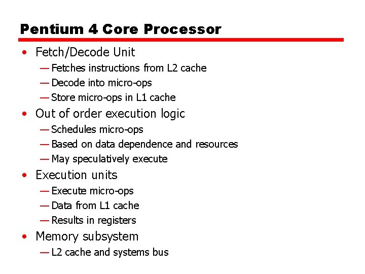
Pentium 4 Core Processor • Fetch/Decode Unit — Fetches instructions from L 2 cache — Decode into micro-ops — Store micro-ops in L 1 cache • Out of order execution logic — Schedules micro-ops — Based on data dependence and resources — May speculatively execute • Execution units — Execute micro-ops — Data from L 1 cache — Results in registers • Memory subsystem — L 2 cache and systems bus

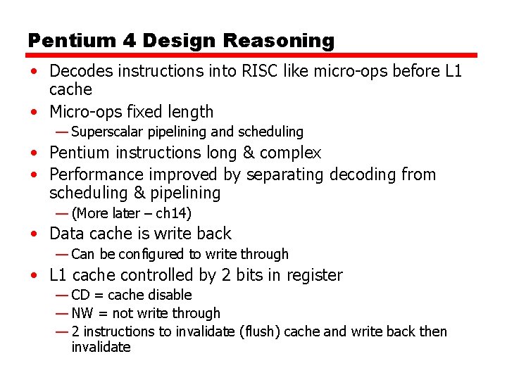
Pentium 4 Design Reasoning • Decodes instructions into RISC like micro-ops before L 1 cache • Micro-ops fixed length — Superscalar pipelining and scheduling • Pentium instructions long & complex • Performance improved by separating decoding from scheduling & pipelining — (More later – ch 14) • Data cache is write back — Can be configured to write through • L 1 cache controlled by 2 bits in register — CD = cache disable — NW = not write through — 2 instructions to invalidate (flush) cache and write back then invalidate

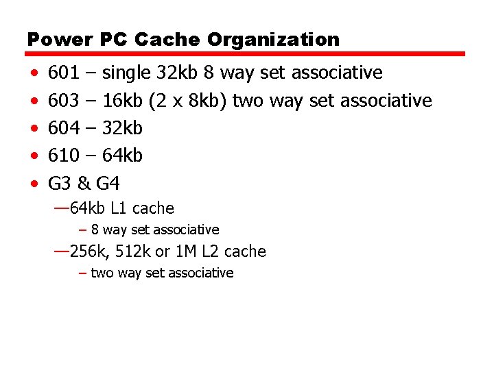
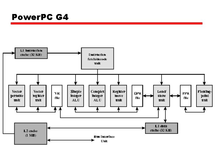
Power PC Cache Organization • • • 601 – single 32 kb 8 way set associative 603 – 16 kb (2 x 8 kb) two way set associative 604 – 32 kb 610 – 64 kb G 3 & G 4 — 64 kb L 1 cache – 8 way set associative — 256 k, 512 k or 1 M L 2 cache – two way set associative

Power. PC G 4

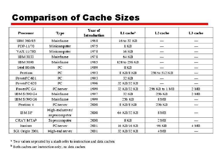
Comparison of Cache Sizes