XFEL DSSC The DSSC project for XFEL DEPFET




- Slides: 70

XFEL DSSC The DSSC project for XFEL: DEPFET and readout ASIC 8 th International Meeting on Front End Electronics Bergamo, 26. 05. 2011 Matteo Porro on behalf of the DSSC Consortium 1 Matteo Porro FEE 2011 Bergamo, 26. 05. 11

XFEL DSSC Consortium M. Porro 1, 2, L. Strueder 1, 2, G. De Vita 1, 2, S. Herrmann 1, 2, D. Muentefering 1, 2, G. Weidenspointner 1, 2, L. Andricek 2, 3, A. Wassatsch 2, 3, P. Lechner 8, G. Lutz 8, C. Sandow 8, S. Aschauer 8, P. Fischer 6, F. Erdinger 6, A. Kugel 6, T. Gerlach 6, K. Hansen 7, C. Reckleben 7, I. Diehl 7, P. Kalavakuru 7, H. Graafsma 7, C. Wunderer 7, H. Hirsemann 7, C. Fiorini 4, 5, L. Bombelli 4, 5, S. Facchinetti 4, 5, A. Castoldi 4, 5, C. Guazzoni 4, 5, D. Mezza 4, 5, V. Re 10, M. Manghisoni 10, U. Pietsch 9, T. Sant 9 1) Max Planck Institut fuer Extraterrestrische Physik, Garching, Germany 2) MPI Halbleiterlabor, Muenchen, Germany 3) Max Planck Institut fuer Physik, Muenchen, Germany 4) Dipartimento di Elettronica e Informazione, Politecnico di Milano, Italy 5) Sezione di Milano, Italian National Institute of Nuclear Physics (INFN), Milano, Italy 6) Zentrales Institut für Technische Informatik, Universitaet Heidelberg, Germany 7) Deutsches Elektronen-Synchrotron DESY, Hamburg, Germany 8) PNSensor Gmb. H, Muenchen, Germany 9) Fachbereich Physik, Universitaet Siegen, Germany 10) Dipartimento di ingegneria industriale, Università di Bergamo, Italy 2 Matteo Porro FEE 2011 Bergamo, 26. 05. 11

XFEL DSSC Outline § Detector Requirements § Detector System Overview § Non-Linear DEPFET Detector working principle § Detector expected performance: • Speed • High Dynamic Range • Single Photon Resolution § ASIC architecture § First experimental results § Conclusions 3 Matteo Porro FEE 2011 Bergamo, 26. 05. 11

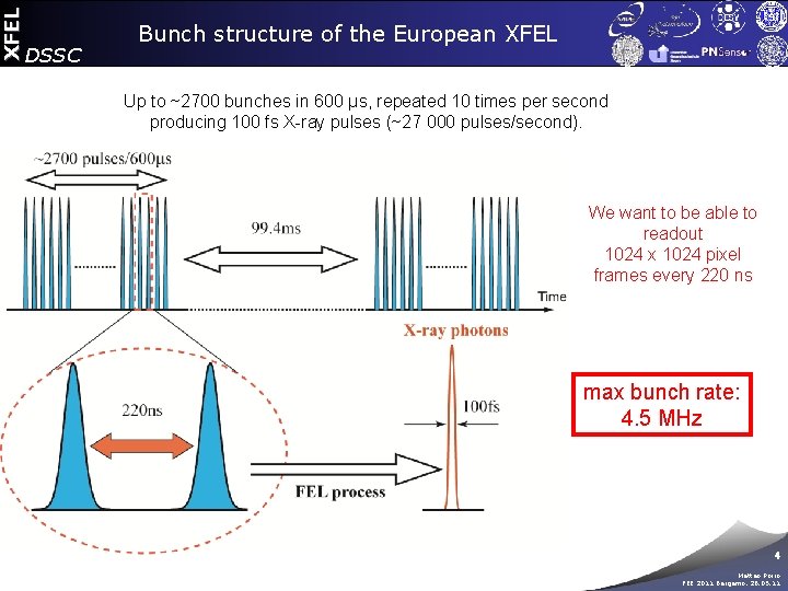
XFEL DSSC Bunch structure of the European XFEL Up to ~2700 bunches in 600 µs, repeated 10 times per second producing 100 fs X-ray pulses (~27 000 pulses/second). We want to be able to readout 1024 x 1024 pixel frames every 220 ns max bunch rate: 4. 5 MHz 4 Matteo Porro FEE 2011 Bergamo, 26. 05. 11

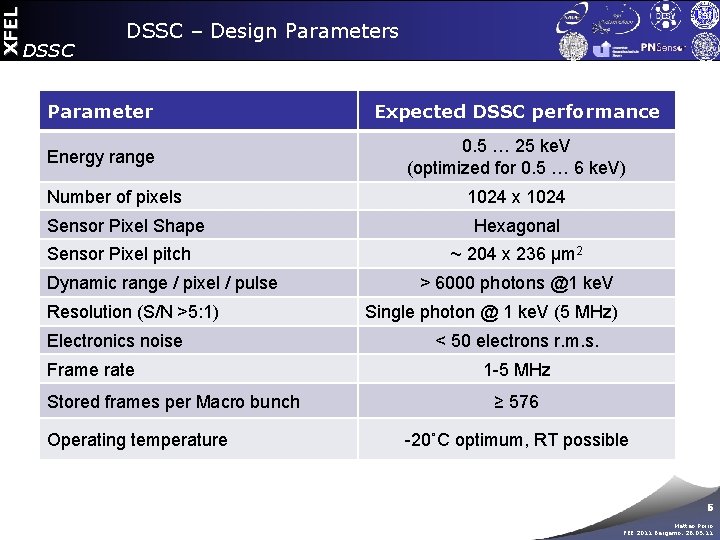
XFEL DSSC – Design Parameters Parameter Expected DSSC performance Energy range 0. 5 … 25 ke. V (optimized for 0. 5 … 6 ke. V) Number of pixels Sensor Pixel Shape Sensor Pixel pitch Dynamic range / pixel / pulse Resolution (S/N >5: 1) Electronics noise Frame rate Stored frames per Macro bunch Operating temperature 1024 x 1024 Hexagonal ~ 204 x 236 µm 2 > 6000 photons @1 ke. V Single photon @ 1 ke. V (5 MHz) < 50 electrons r. m. s. 1 -5 MHz ≥ 576 -20˚C optimum, RT possible 5 Matteo Porro FEE 2011 Bergamo, 26. 05. 11

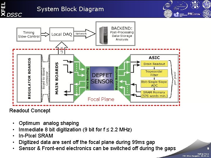
XFEL DSSC System Block Diagram Focal Plane Readout Concept • • • Optimum analog shaping Immediate 8 bit digitization (9 bit for f ≤ 2. 2 MHz) In-Pixel SRAM Digitized data are sent off the focal plane during 99 ms gap Sensor & Front-end electronics can be switched off during the gaps 6 Matteo Porro FEE 2011 Bergamo, 26. 05. 11

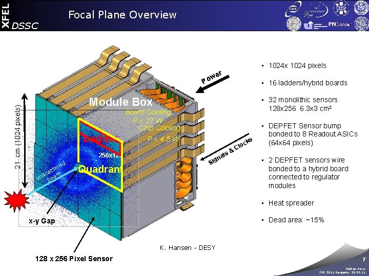
DSSC w Po 21 cm (1024 pixels) XFEL Focal Plane Overview • 1024 x 1024 pixels er • 16 ladders/hybrid boards • 32 monolithic sensors 128 x 256 6. 3 x 3 cm 2 Module Box Board Cooling P < 27 W Chip Cooling Ladder 256 x 128 d ere t t a sc m un bea Quadrant P < 4. 5 W ks ls na Sig & c Clo • DEPFET Sensor bump bonded to 8 Readout ASICs (64 x 64 pixels) • 2 DEPFET sensors wire bonded to a hybrid board connected to regulator modules • Heat spreader • Dead area: ~15% x-y Gap K. Hansen - DESY 128 x 256 Pixel Sensor 7 Matteo Porro FEE 2011 Bergamo, 26. 05. 11

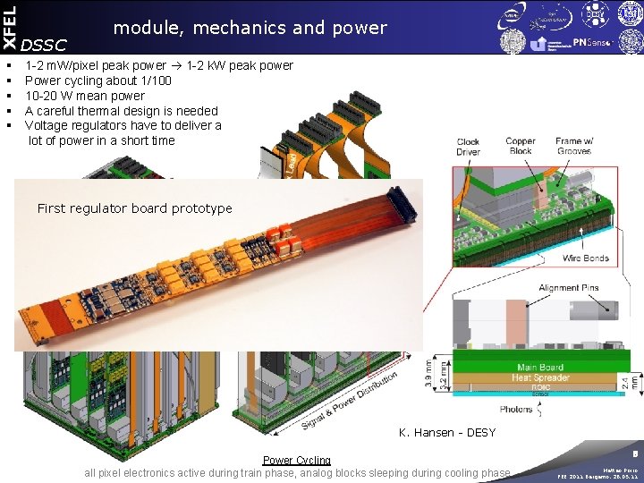
XFEL § § § module, mechanics and power DSSC 1 -2 m. W/pixel peak power 1 -2 k. W peak power Power cycling about 1/100 10 -20 W mean power A careful thermal design is needed Voltage regulators have to deliver a lot of power in a short time First regulator board prototype ~3 mm K. Hansen - DESY Power Cycling all pixel electronics active during train phase, analog blocks sleeping during cooling phase 8 Matteo Porro FEE 2011 Bergamo, 26. 05. 11

XFEL DSSC - Concept ● DEPFET Active Pixel Sensor is the first element of the Front-end Electronics ● Every DEPFET pixel provides detection and amplification with: § Low noise § Signal compression at the sensor level § High speed (fully parallel readout at 1 -5 MHz) 9 Matteo Porro FEE 2011 Bergamo, 26. 05. 11

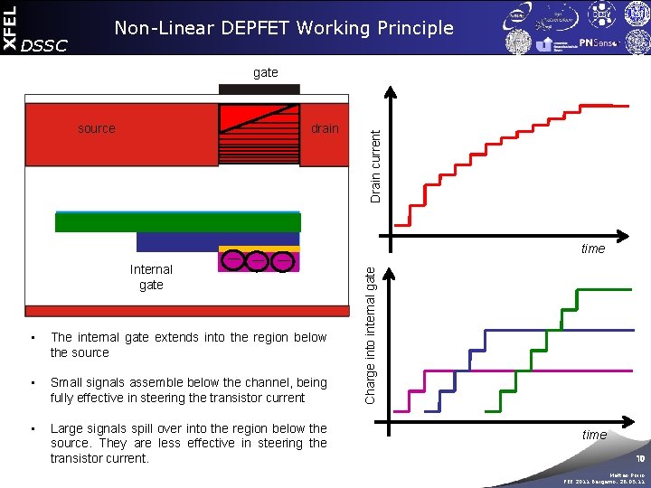
source drain Drain current gate time Internal gate • The internal gate extends into the region below §the source A constant charge is injected at fixed time intervals and the internal gate regions are progressively filled • Small signals assemble below the channel, being fully effective in steering the transistor current • In the experiment the charge is Large signals spill over into the region below the deposited at once but the DEPFET source. They are less effective in steering the response is the same Charge into internal gate XFEL DSSC Non-Linear DEPFET Working Principle § transistor current. time 10 Matteo Porro FEE 2011 Bergamo, 26. 05. 11

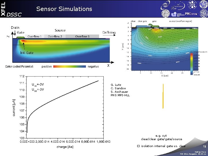
XFEL DSSC Sensor Simulations G. Lutz C. Sandow S. Aschauer PNS MPI-HLL e. g. cut clear/clear gate/source � isolation internal gate vs. clear 11 Matteo Porro FEE 2011 Bergamo, 26. 05. 11

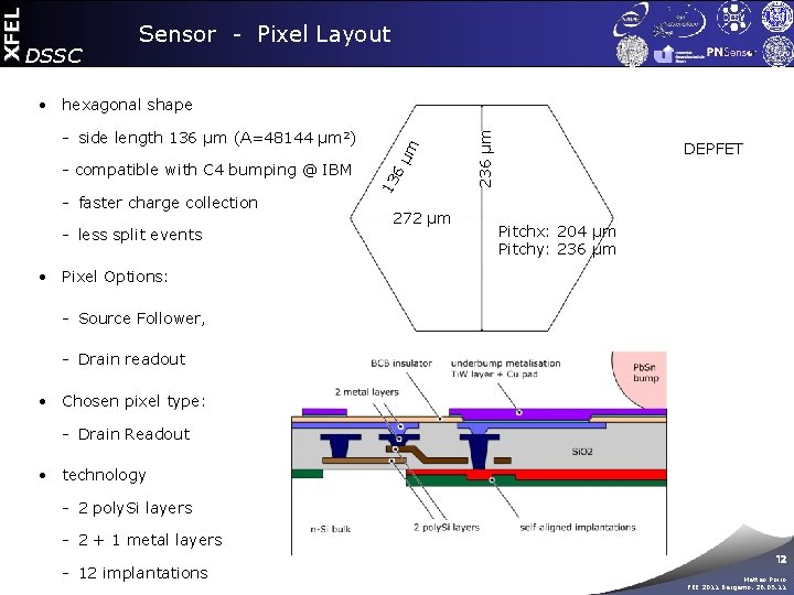
- faster charge collection - less split events 272 µm 236 µm - compatible with C 4 bumping @ IBM 6 µ - side length 136 µm (A=48144 µm 2) m • hexagonal shape 13 XFEL DSSC Sensor - Pixel Layout DEPFET Pitchx: 204 µm Pitchy: 236 µm • Pixel Options: - Source Follower, - Drain readout • Chosen pixel type: - Drain Readout • technology - 2 poly. Si layers - 2 + 1 metal layers - 12 implantations 12 Matteo Porro FEE 2011 Bergamo, 26. 05. 11

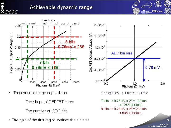
XFEL DSSC Achievable dynamic range 8 bits 0. 78 m. V x 256 7 bits 0. 78 m. V x 128 • The dynamic range depends on: The shape of DEPFET curve The number of ADC bits • The gain of the first region defines the bin size 1 ph @1 ke. V 1 bin = 0. 78 m. V 7 bits 0. 78 m. V x 27 = 100 m. V 1245 photons 8 bits 0. 78 m. V x 28 = 200 m. V 5850 photons 13 Matteo Porro FEE 2011 Bergamo, 26. 05. 11

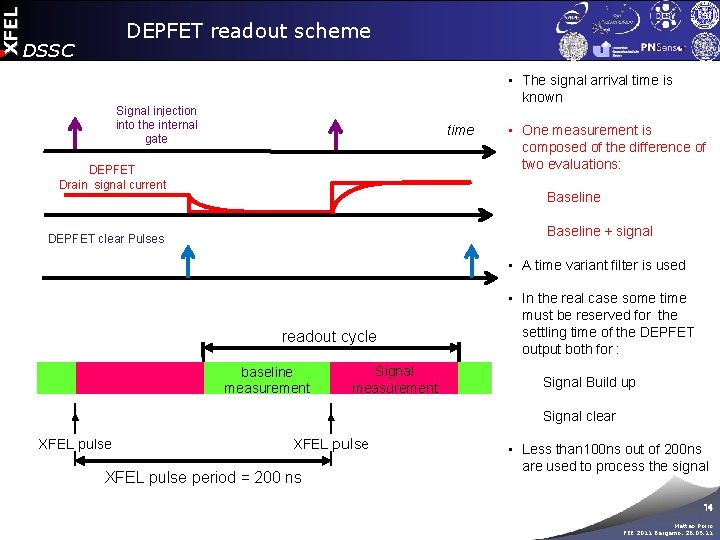
XFEL DEPFET readout scheme DSSC • The signal arrival time is known Signal injection into the internal gate time DEPFET Drain signal current • One measurement is composed of the difference of two evaluations: Baseline + signal DEPFET clear Pulses • A time variant filter is used filtering process (e. g. triangular weighting function) readout cycle baseline clear baseline measurement DEPFET measurement signal. Signal measurement settling measurement • In the real case some time must be reserved for the settling time of the DEPFET output both for : Signal Build up Signal clear XFEL pulse period = 200 ns • Less than 100 ns out of 200 ns are used to process the signal 14 Matteo Porro FEE 2011 Bergamo, 26. 05. 11

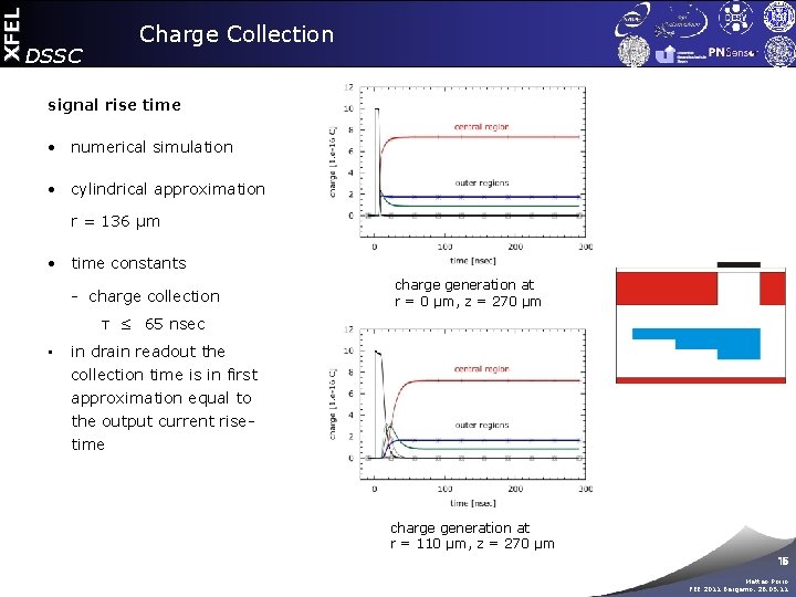
XFEL DSSC Charge Collection signal rise time • numerical simulation • cylindrical approximation r = 136 µm • time constants - charge collection charge generation at r = 0 µm, z = 270 µm τ ≤ 65 nsec • in drain readout the collection time is in first approximation equal to the output current risetime charge generation at r = 110 µm, z = 270 µm 15 Matteo Porro FEE 2011 Bergamo, 26. 05. 11

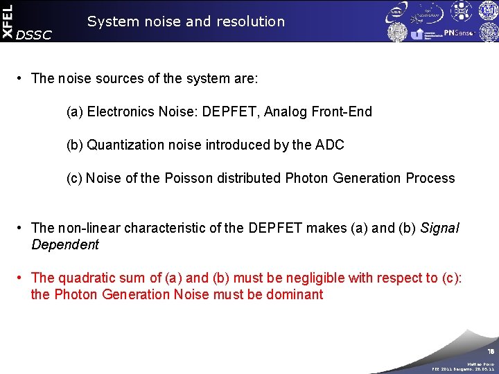
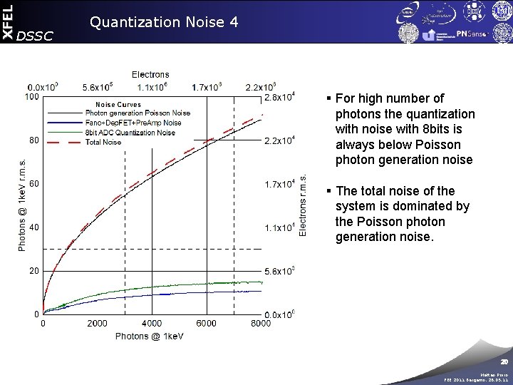
XFEL DSSC System noise and resolution • The noise sources of the system are: (a) Electronics Noise: DEPFET, Analog Front-End (b) Quantization noise introduced by the ADC (c) Noise of the Poisson distributed Photon Generation Process • The non-linear characteristic of the DEPFET makes (a) and (b) Signal Dependent • The quadratic sum of (a) and (b) must be negligible with respect to (c): the Photon Generation Noise must be dominant 16 Matteo Porro FEE 2011 Bergamo, 26. 05. 11

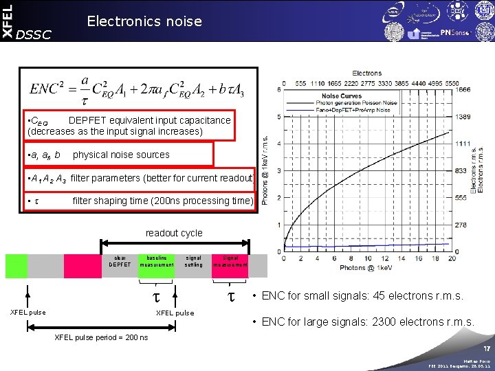
XFEL Electronics noise DSSC • CEQ DEPFET equivalent input capacitance (decreases as the input signal increases) • a, af, b physical noise sources • A 1 A 2 A 3 filter parameters (better for current readout) • t filter shaping time (200 ns processing time) § The noise sources are almost readout cycle constant From sensor simulations § The amplification decreases as clear DEPFET baseline measurement the input signal increases signal settling 55 f. F. . . 3200 f. F t Signal measurement § The ENC increases with the input signal amplitude XFEL pulse t • ENC for small signals: 45 electrons r. m. s. • ENC for large signals: 2300 electrons r. m. s. XFEL pulse period = 200 ns 17 Matteo Porro FEE 2011 Bergamo, 26. 05. 11

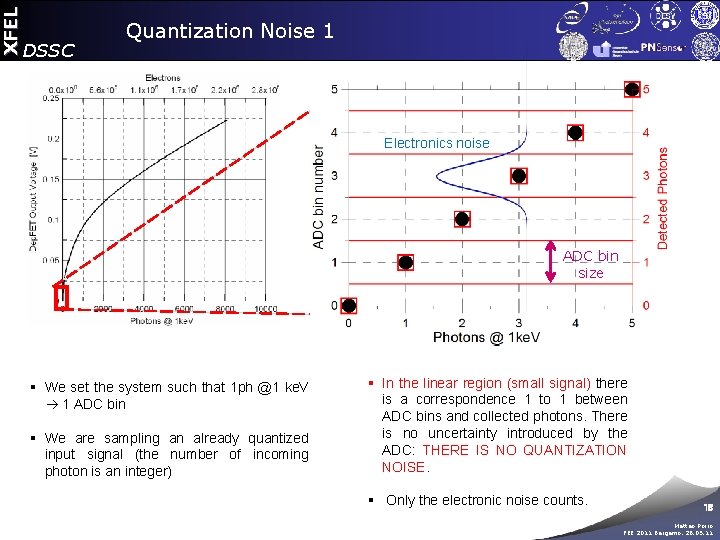
XFEL DSSC Quantization Noise 1 Electronics noise ADC bin size § We set the system such that 1 ph @1 ke. V 1 ADC bin § We are sampling an already quantized input signal (the number of incoming photon is an integer) § In the linear region (small signal) there is a correspondence 1 to 1 between ADC bins and collected photons. There is no uncertainty introduced by the ADC: THERE IS NO QUANTIZATION NOISE. § Only the electronic noise counts. 18 Matteo Porro FEE 2011 Bergamo, 26. 05. 11

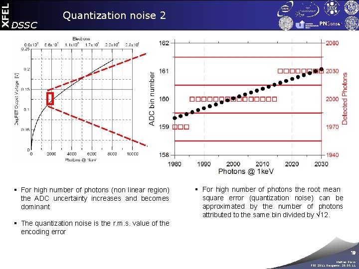
XFEL DSSC Quantization noise 2 § For high number of photons (non linear region) the ADC uncertainty increases and becomes dominant § For high number of photons the root mean square error (quantization noise) can be approximated by the number of photons attributed to the same bin divided by 12. § The quantization noise is the r. m. s. value of the encoding error 19 Matteo Porro FEE 2011 Bergamo, 26. 05. 11

XFEL DSSC Quantization Noise 4 § For high number of photons the quantization with noise with 8 bits is always below Poisson photon generation noise § The total noise of the system is dominated by the Poisson photon generation noise. 20 Matteo Porro FEE 2011 Bergamo, 26. 05. 11

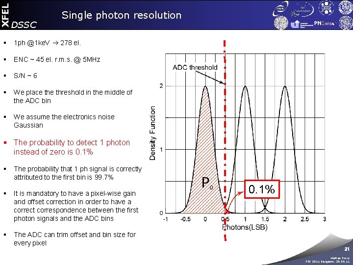
XFEL DSSC Single photon resolution § 1 ph @1 ke. V 278 el. § ENC ~ 45 el. r. m. s. @ 5 MHz § S/N ~ 6 § We place threshold in the middle of the ADC bin § We assume the electronics noise Gaussian § The probability to detect 1 photon instead of zero is 0. 1% § The probability that 1 ph signal is correctly attributed to the first bin is 99. 7% § It is mandatory to have a pixel-wise gain and offset correction in order to have a correct correspondence between the first photon signals and the ADC bins 0. 1% § The ADC can trim offset and bin size for every pixel 21 Matteo Porro FEE 2011 Bergamo, 26. 05. 11

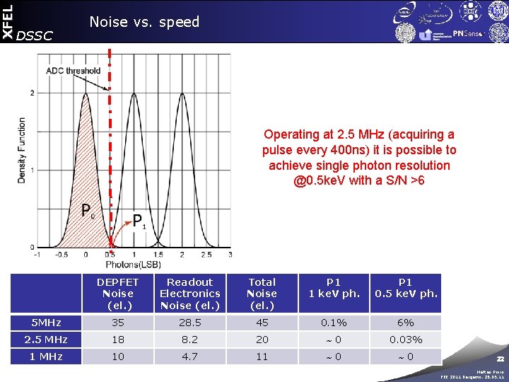
XFEL DSSC Noise vs. speed Operating at 2. 5 MHz (acquiring a pulse every 400 ns) it is possible to achieve single photon resolution @0. 5 ke. V with a S/N >6 DEPFET Noise (el. ) Readout Electronics Noise (el. ) Total Noise (el. ) P 1 1 ke. V ph. P 1 0. 5 ke. V ph. 5 MHz 35 28. 5 45 0. 1% 6% 2. 5 MHz 18 8. 2 20 0 0. 03% 1 MHz 10 4. 7 11 0 0 22 Matteo Porro FEE 2011 Bergamo, 26. 05. 11

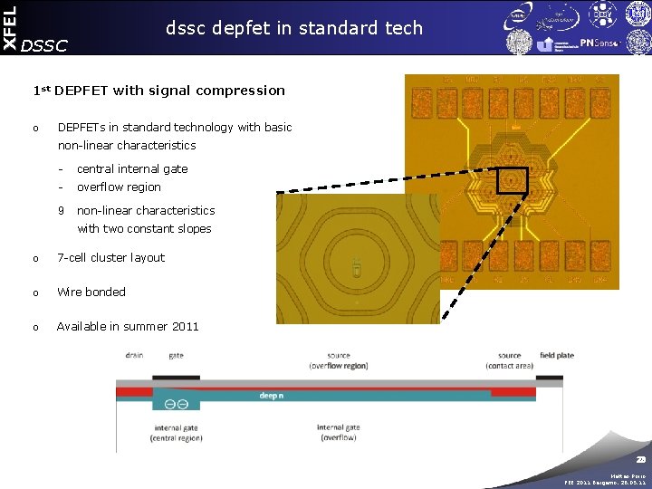
XFEL dssc depfet in standard tech DSSC 1 st DEPFET with signal compression o DEPFETs in standard technology with basic non-linear characteristics - central internal gate - overflow region 9 non-linear characteristics with two constant slopes o 7 -cell cluster layout o Wire bonded o Available in summer 2011 23 Matteo Porro FEE 2011 Bergamo, 26. 05. 11

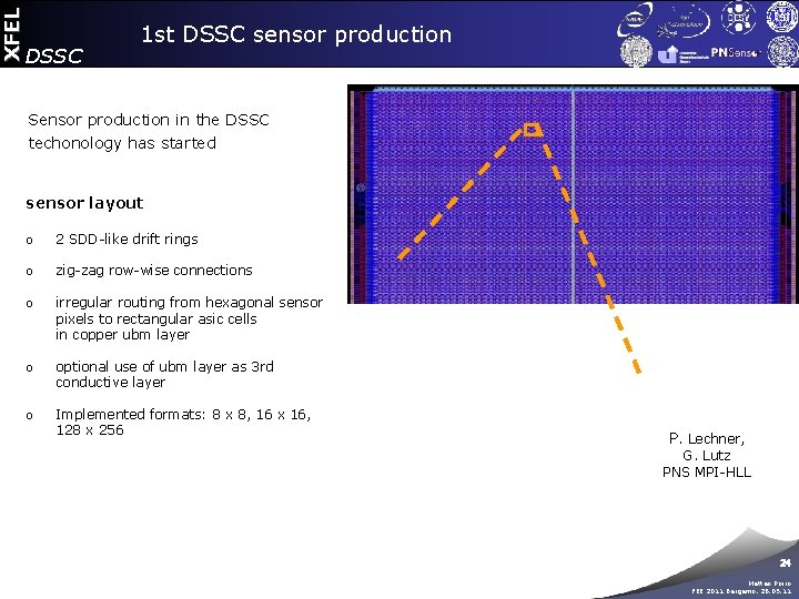
XFEL DSSC 1 st DSSC sensor production Sensor production in the DSSC techonology has started sensor layout o 2 SDD-like drift rings o zig-zag row-wise connections o irregular routing from hexagonal sensor pixels to rectangular asic cells in copper ubm layer o optional use of ubm layer as 3 rd conductive layer o Implemented formats: 8 x 8, 16 x 16, 128 x 256 DSSC layout detail P. Lechner, G. Lutz PNS MPI-HLL 24 Matteo Porro FEE 2011 Bergamo, 26. 05. 11

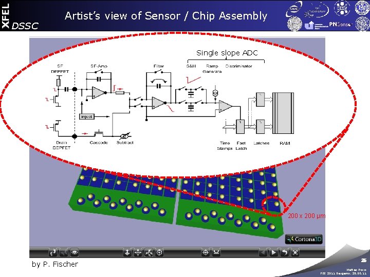
XFEL DSSC Artist’s view of Sensor / Chip Assembly Single slope ADC 200 x 200 µm by P. Fischer 25 Matteo Porro FEE 2011 Bergamo, 26. 05. 11

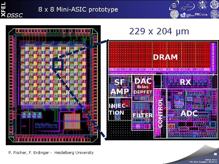
XFEL DSSC 8 x 8 Mini-ASIC prototype 229 x 204 µm P. Fischer, F. Erdinger - Heidelberg University 26 Matteo Porro FEE 2011 Bergamo, 26. 05. 11

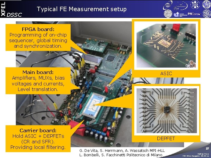
XFEL DSSC Typical FE Measurement setup FPGA board: Programming of on-chip sequencer, global timing and synchronization. Main board: Amplifiers, MUXs, bias voltages and currents, Level translation. Carrier board: Hold ASIC + DEPFETs (CR and SFR). Providing local filtering. ASIC DEPFET G. De Vita, S. Herrmann, A. Wassatsch MPI-HLL L. Bombelli, S. Facchinetti Politecnico di Milano 27 Matteo Porro FEE 2011 Bergamo, 26. 05. 11

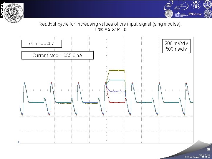
XFEL DSSC Readout cycle for increasing values of the input signal (single pulse). Freq = 2. 57 MHz Gext = - 4. 7 200 m. V/div 500 ns/div Current step = 635. 6 n. A 28 Matteo Porro FEE 2011 Bergamo, 26. 05. 11

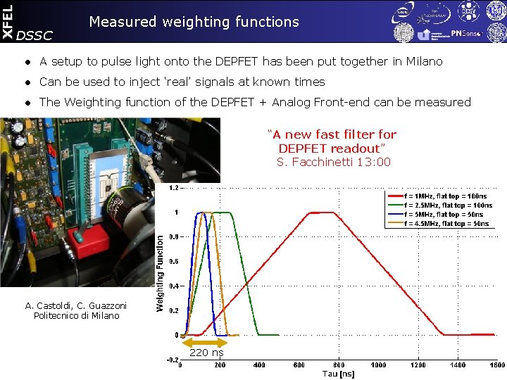
XFEL DSSC Measured weighting functions ● A setup to pulse light onto the DEPFET has been put together in Milano ● Can be used to inject ‘real’ signals at known times ● The Weighting function of the DEPFET + Analog Front-end can be measured “A new fast filter for DEPFET readout” S. Facchinetti 13: 00 A. Castoldi, C. Guazzoni Politecnico di Milano 220 ns 29 Matteo Porro FEE 2011 Bergamo, 26. 05. 11

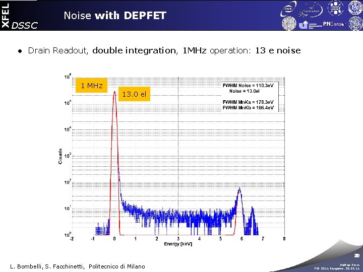
XFEL DSSC Noise with DEPFET ● Drain Readout, double integration, 1 MHz operation: 13 e noise 1 MHz 13. 0 el 30 L. Bombelli, S. Facchinetti, Politecnico di Milano Matteo Porro FEE 2011 Bergamo, 26. 05. 11

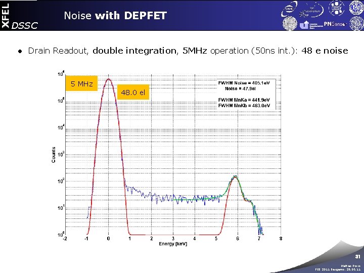
XFEL DSSC Noise with DEPFET ● Drain Readout, double integration, 5 MHz operation (50 ns int. ): 48 e noise 5 MHz 48. 0 el 31 Matteo Porro FEE 2011 Bergamo, 26. 05. 11

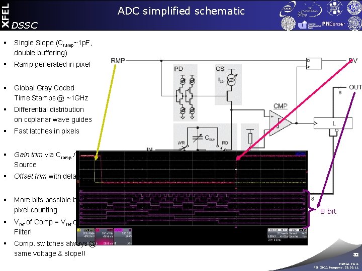
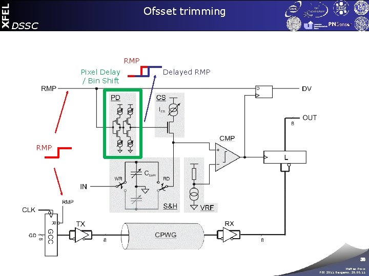
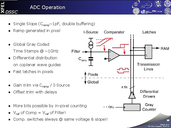
XFEL ADC simplified schematic DSSC § Single Slope (Cramp~1 p. F, double buffering) § Ramp generated in pixel § Global Gray Coded Time Stamps @ ~1 GHz § Differential distribution on coplanar wave guides § Fast latches in pixels § Gain trim via Cramp / ISource § Offset trim with delays § More bits possible by inpixel counting 8 bit § Vref of Comp = Vref of Filter! § Comp. switches always @ same voltage & slope!! 32 Matteo Porro FEE 2011 Bergamo, 26. 05. 11

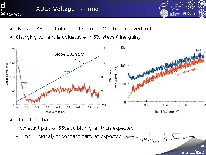
XFEL DSSC ADC: Voltage → Time ● INL < 1 LSB (limit of current source). Can be improved further. ● Charging current is adjustable in 5% steps (fine gain) Slope 201 ns/V ● Time Jitter has - constant part of 55 ps (a bit higher than expected) - Time (=signal) dependant part, as expected 33 Matteo Porro FEE 2011 Bergamo, 26. 05. 11

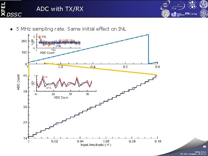
XFEL DSSC ADC with TX/RX ● 5 MHz sampling rate. Same initial effect on INL 34 Matteo Porro FEE 2011 Bergamo, 26. 05. 11

XFEL DSSC STEP 1: OFFSET ADJUSTMENT IF NOISE « BIN SIZE: BIN SCAN Zero-signal bin Bin 0 after offset adjustment Bin 1 Bin 2 CBIN 0=0 CBIN 1=1 CBIN 2=0 Bin size COffset granularity BIN 0=0 CBIN 1=1 CBIN 2=0 CBIN 0=0 CBIN 1=1 CBIN 2=0 Upper boundary CBIN 0=0 CBIN 1=0 CBIN 2=1 CBIN 0=0 CBIN 1=1 CBIN 2=0 Lower boundary CBIN 0=1 CBIN 1=0 CBIN 2=0 35 Matteo Porro FEE 2011 Bergamo, 26. 05. 11

XFEL Ofsset trimming DSSC RMP Pixel Delay / Bin Shift Delayed RMP 36 Matteo Porro FEE 2011 Bergamo, 26. 05. 11

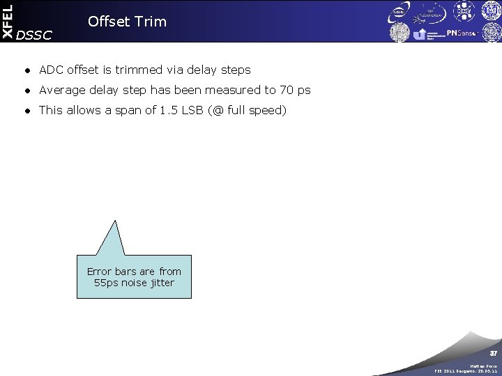
XFEL DSSC Offset Trim ● ADC offset is trimmed via delay steps ● Average delay step has been measured to 70 ps ● This allows a span of 1. 5 LSB (@ full speed) Error bars are from 55 ps noise jitter 37 Matteo Porro FEE 2011 Bergamo, 26. 05. 11

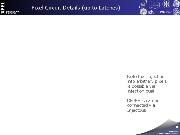
XFEL DSSC Pixel Circuit Details (up to Latches) Note that injection into arbitrary pixels is possible via injection bus! DEPFETs can be connected via Injectbus 38 Matteo Porro FEE 2011 Bergamo, 26. 05. 11

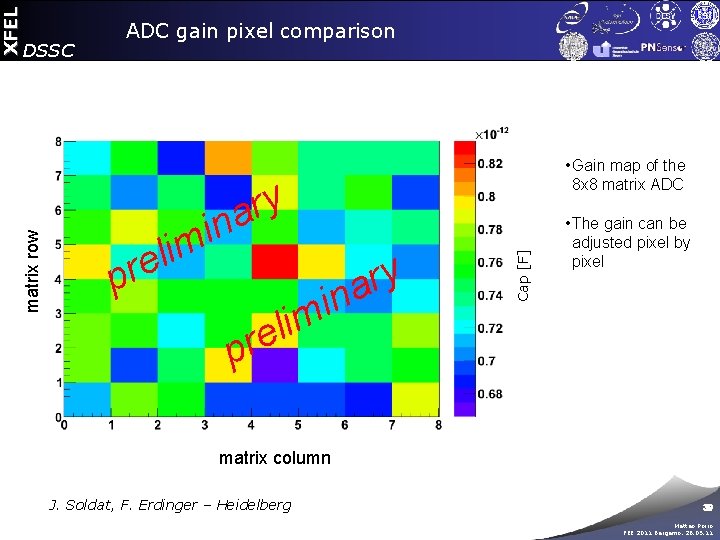
• Gain map of the 8 x 8 matrix ADC y r a n i im l e pr y r a n mi i l e r p Cap [F] matrix row XFEL DSSC ADC gain pixel comparison • The gain can be adjusted pixel by pixel matrix column J. Soldat, F. Erdinger – Heidelberg 39 Matteo Porro FEE 2011 Bergamo, 26. 05. 11

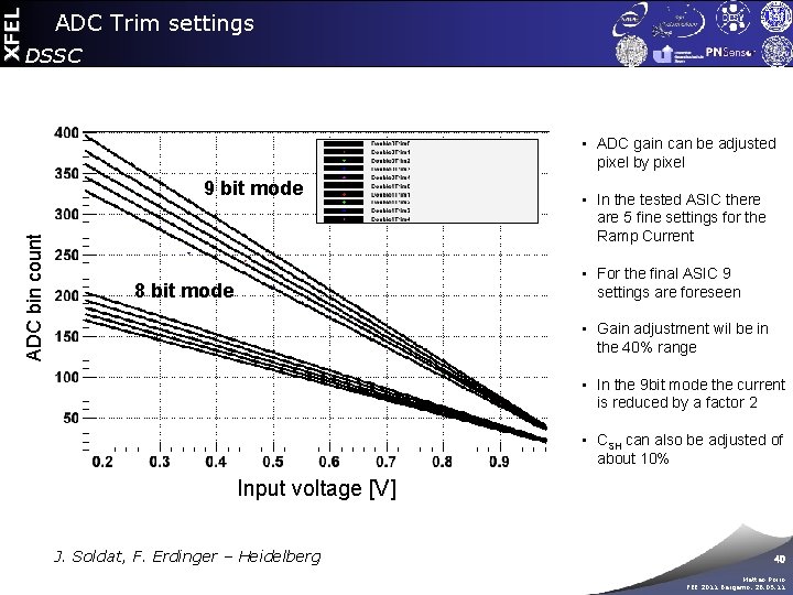
XFEL ADC Trim settings DSSC • ADC gain can be adjusted pixel by pixel ADC bin count 9 bit mode • In the tested ASIC there are 5 fine settings for the Ramp Current • For the final ASIC 9 settings are foreseen 8 bit mode • Gain adjustment wil be in the 40% range • In the 9 bit mode the current is reduced by a factor 2 • CSH can also be adjusted of about 10% Input voltage [V] J. Soldat, F. Erdinger – Heidelberg 40 Matteo Porro FEE 2011 Bergamo, 26. 05. 11

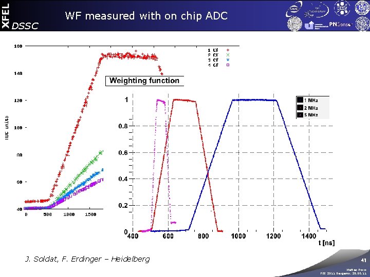
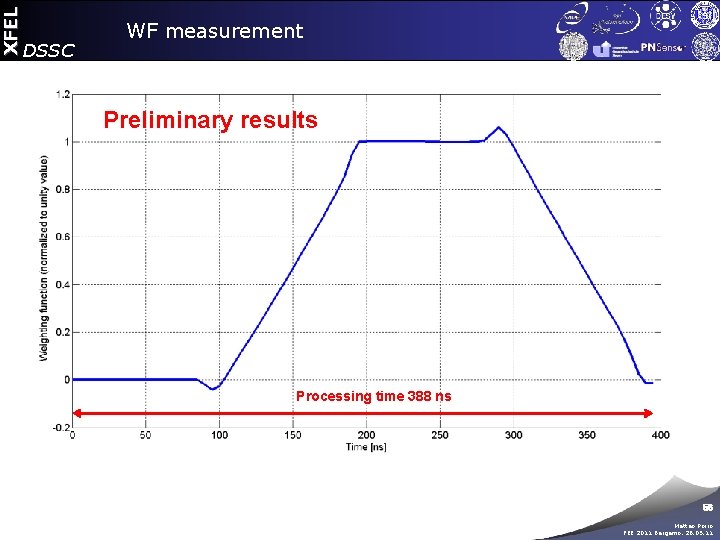
XFEL DSSC WF measured with on chip ADC J. Soldat, F. Erdinger – Heidelberg 41 Matteo Porro FEE 2011 Bergamo, 26. 05. 11

XFEL DSSC Summary & Conclusions § We are developing a Pixel Detector system for the European XFEL based on innovative non-linear DEPFET devices that constitute the first element of the Frontend Electronics § In our fully parallel readout scheme, the signals coming from the pixels are filtered, digitized and stored in the focal plane § Device and circuit simulations have shown that: • It is possible to achieve 5 MHz frame readout • A dynamic range of at least 6000 Photons at 1 ke. V per pixel is possible • A single 1 ke. V photon resolution (S/N>6) is reachable @ 5 MHz preserving the high dynamic range • Also single 0. 5 ke. V photon resolution is achievable @ 2. 5 Mhz § Measurements on first ASIC blocks show performance in good agreement with simulations and a noise below 50 el. r. m. s. At the maximum operating speed § First DEPFET with signal compression will be available soon § The first DSSC Sensor production comprising full-size sensors has started 42 Matteo Porro FEE 2011 Bergamo, 26. 05. 11

XFEL DSSC SPARE SLIDES 43 Matteo Porro FEE 2011 Bergamo, 26. 05. 11

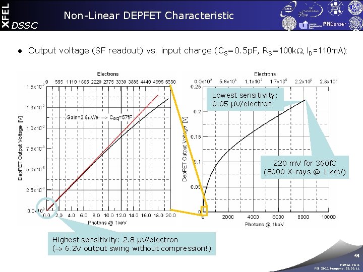
XFEL DSSC Non-Linear DEPFET Characteristic ● Output voltage (SF readout) vs. input charge (CS=0. 5 p. F, RS=100 k , ID=110 m. A): Lowest sensitivity: 0. 05 µV/electron 220 m. V for 360 f. C (8000 X-rays @ 1 ke. V) Highest sensitivity: 2. 8 µV/electron ( 6. 2 V output swing without compression!) 44 Matteo Porro FEE 2011 Bergamo, 26. 05. 11

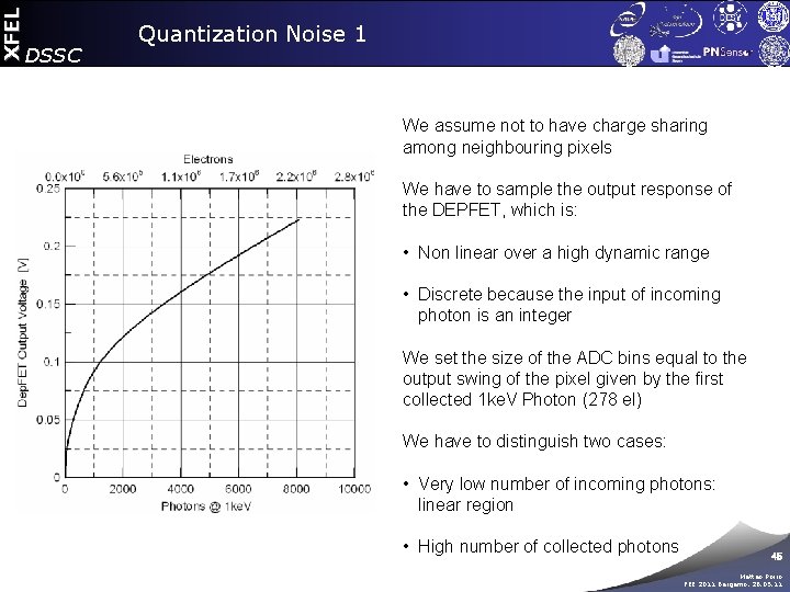
XFEL DSSC Quantization Noise 1 We assume not to have charge sharing among neighbouring pixels We have to sample the output response of the DEPFET, which is: • Non linear over a high dynamic range • Discrete because the input of incoming photon is an integer We set the size of the ADC bins equal to the output swing of the pixel given by the first collected 1 ke. V Photon (278 el) We have to distinguish two cases: • Very low number of incoming photons: linear region • High number of collected photons 45 Matteo Porro FEE 2011 Bergamo, 26. 05. 11

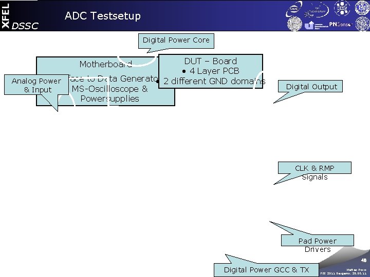
XFEL DSSC ADC Testsetup Digital Power Core DUT – Board • 4 Layer PCB Interface to Data Generator, Analog Power • 2 different GND domains MS-Oscilloscope & & Input Powersupplies Motherboard Digital Output ADC Decoupling Caps CLK & RMP Signals Pad Power Drivers 46 Digital Power GCC & TX Matteo Porro FEE 2011 Bergamo, 26. 05. 11

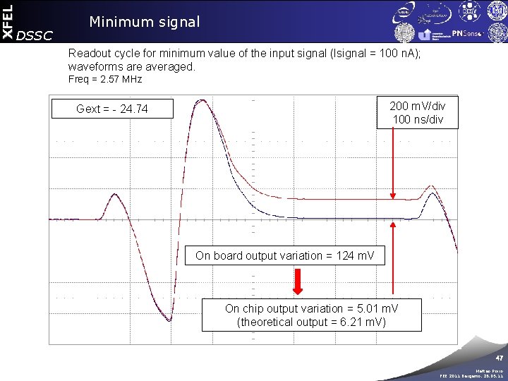
XFEL DSSC Minimum signal Readout cycle for minimum value of the input signal (Isignal = 100 n. A); waveforms are averaged. Freq = 2. 57 MHz 200 m. V/div 100 ns/div Gext = - 24. 74 On board output variation = 124 m. V On chip output variation = 5. 01 m. V (theoretical output = 6. 21 m. V) 47 Matteo Porro FEE 2011 Bergamo, 26. 05. 11

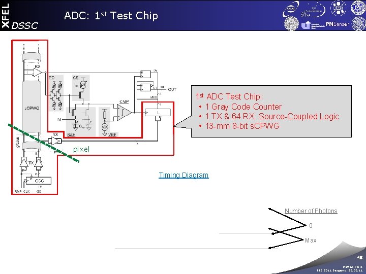
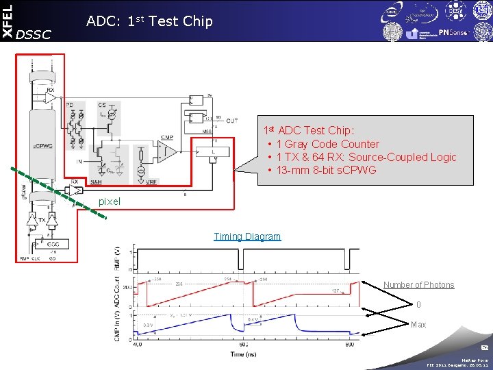
XFEL DSSC ADC: 1 st Test Chip 1 st ADC Test Chip: • 1 Gray Code Counter • 1 TX & 64 RX: Source-Coupled Logic • 13 -mm 8 -bit s. CPWG pixel Timing Diagram Number of Photons 0 Max 48 Matteo Porro FEE 2011 Bergamo, 26. 05. 11

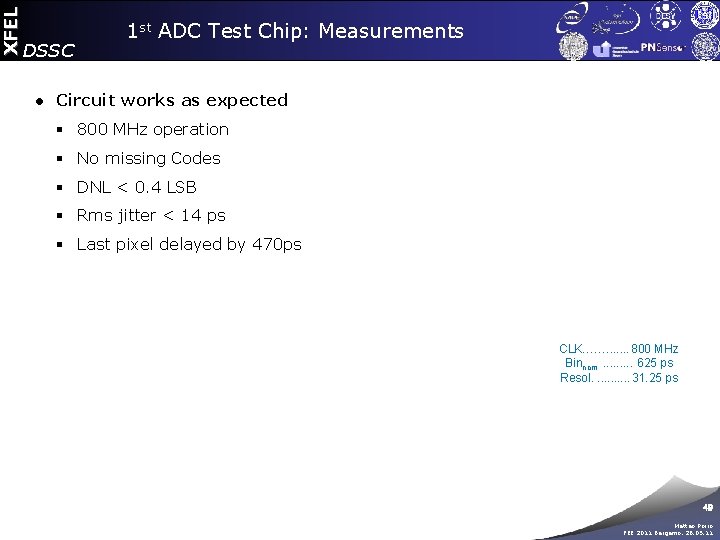
XFEL DSSC 1 st ADC Test Chip: Measurements ● Circuit works as expected § 800 MHz operation § No missing Codes § DNL < 0. 4 LSB § Rms jitter < 14 ps § Last pixel delayed by 470 ps CLK……. . . . 800 MHz Binnom . . 625 ps Resol. . . 31. 25 ps 49 Matteo Porro FEE 2011 Bergamo, 26. 05. 11

XFEL DSSC ADC Operation ● Single Slope (Cramp~1 p. F, double buffering) ● Ramp generated in pixel ● Global Gray Coded Time Stamps @ ~1 GHz ● Differential distribution on coplanar wave guides ● Fast latches in pixels ● Gain trim via Cramp / I-Source ● Offset trim with delays ● More bits possible by in-pixel counting ● Vref of Comp = Vref of Filter! ● Comp. switches always @ same voltage & slope!! 50 Matteo Porro FEE 2011 Bergamo, 26. 05. 11

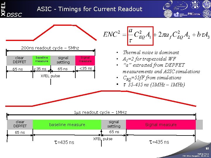
XFEL DSSC ASIC - Timings for Current Readout 200 ns readout cycle – 5 Mhz clear DEPFET 65 ns baseline measure <35 ns signal settling Signal measure 65 ns <35 ns • Thermal noise is dominant • A 1=2 for trapezoidal WF • “a” extracted from DEPFET measurements and ASIC simulations • CEQ=55 f. F from simulations • t 35 -435 ns (5 MHz – 1 MHz) XFEL pulse 1 ms readout cycle – 1 MHz clear DEPFET baseline measure signal settling Signal measure 65 ns t=435 ns XFEL pulse t=435 ns 51 Matteo Porro FEE 2011 Bergamo, 26. 05. 11

XFEL DSSC ADC: 1 st Test Chip 1 st ADC Test Chip: • 1 Gray Code Counter • 1 TX & 64 RX: Source-Coupled Logic • 13 -mm 8 -bit s. CPWG pixel Timing Diagram Number of Photons 0 Max 52 Matteo Porro FEE 2011 Bergamo, 26. 05. 11

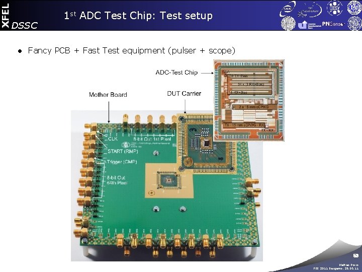
XFEL DSSC 1 st ADC Test Chip: Test setup ● Fancy PCB + Fast Test equipment (pulser + scope) 53 Matteo Porro FEE 2011 Bergamo, 26. 05. 11

XFEL DSSC 1 st ADC Test Chip: Measurements ● Circuit works as expected § 800 MHz operation § No missing Codes § DNL < 0. 4 LSB § Rms jitter < 14 ps § Last pixel delayed by 470 ps CLK……. . . . 800 MHz Binnom . . 625 ps Resol. . . 31. 25 ps 54 Matteo Porro FEE 2011 Bergamo, 26. 05. 11

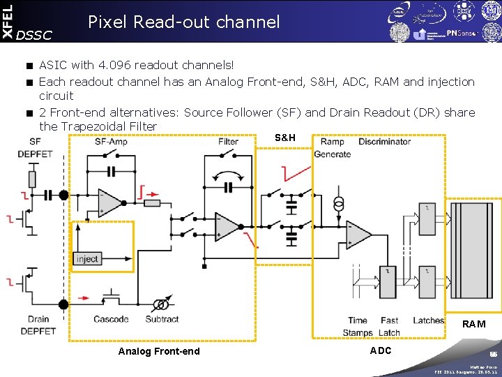
XFEL DSSC Pixel Read-out channel ASIC with 4. 096 readout channels! Each readout channel has an Analog Front-end, S&H, ADC, RAM and injection circuit 2 Front-end alternatives: Source Follower (SF) and Drain Readout (DR) share the Trapezoidal Filter S&H RAM Analog Front-end ADC 55 Matteo Porro FEE 2011 Bergamo, 26. 05. 11

XFEL DSSC WF measurement Preliminary results Processing time 388 ns 56 Matteo Porro FEE 2011 Bergamo, 26. 05. 11

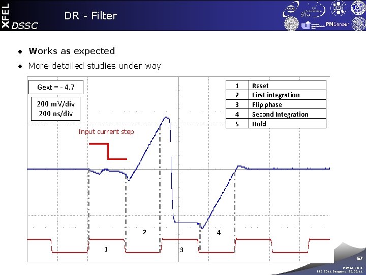
XFEL DSSC DR - Filter ● Works as expected ● More detailed studies under way 1 2 3 4 5 Gext = - 4. 7 200 m. V/div 200 ns/div Input current step 2 1 Reset First integration Flip phase Second Integration Hold 4 3 57 Matteo Porro FEE 2011 Bergamo, 26. 05. 11

XFEL DSSC 1 st ADC Test Chip: Measurements ● Circuit works as expected § 800 MHz operation § No missing Codes § DNL < 0. 4 LSB § Rms jitter < 14 ps § Last pixel delayed by 470 ps CLK……. . . . 800 MHz Binnom . . 625 ps Resol. . . 31. 25 ps 58 Matteo Porro FEE 2011 Bergamo, 26. 05. 11

XFEL DSSC ADC: Reminder of Concept ● Single Slope ADC § successfully used in multi-ADC applications: § very simple architecture § minimal analog content § shared functionalities Tedja et al. , IEEE SSC 1995 Yang et al. , CICC 1998 Kleinfelder et al. , IEEE SSC 2001 Hwang et al. , SPIE 2007 Varner et al. , NIMA 2007 Delagnes et al. , IEEE TNS 2007 Da Silva et al. , IEEE NSS 2007 Crooks et al. , IEEE Sensors 2008 § minimal area requirements (per channel) ● In our case: § Local ramp generation § Time stamp distribution on shielded coplanar waveguides using differential signals 59 Matteo Porro FEE 2011 Bergamo, 26. 05. 11

XFEL DSSC ADC: 1 st Test Chip 1 st ADC Test Chip: • 1 Gray Code Counter • 1 TX & 64 RX: Source-Coupled Logic • 13 -mm 8 -bit s. CPWG pixel Timing Diagram Number of Photons 0 Max 60 Matteo Porro FEE 2011 Bergamo, 26. 05. 11

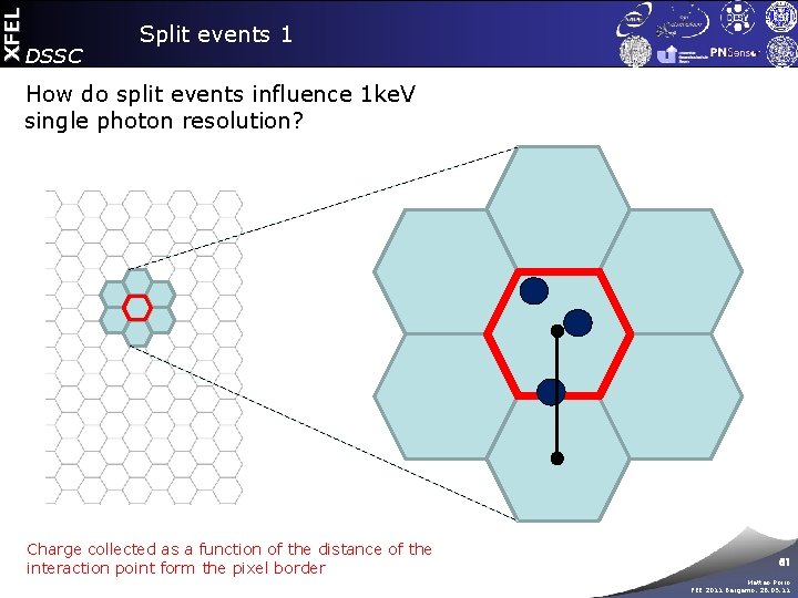
XFEL DSSC Split events 1 How do split events influence 1 ke. V single photon resolution? Charge collected as a function of the distance of the interaction point form the pixel border 61 Matteo Porro FEE 2011 Bergamo, 26. 05. 11

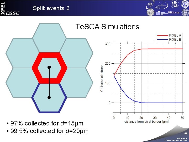
XFEL DSSC Split events 2 Te. SCA Simulations • 97% collected for d=15µm • 99. 5% collected for d=20µm 62 Matteo Porro FEE 2011 Bergamo, 26. 05. 11

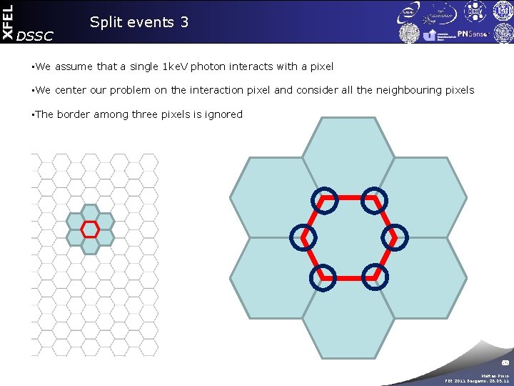
XFEL DSSC Split events 3 • We assume that a single 1 ke. V photon interacts with a pixel • We center our problem on the interaction pixel and consider all the neighbouring pixels • The border among three pixels is ignored 63 Matteo Porro FEE 2011 Bergamo, 26. 05. 11

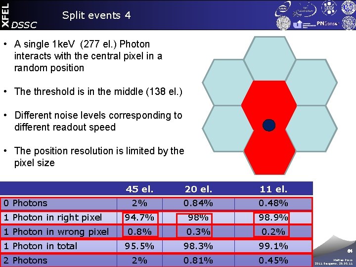
XFEL DSSC Split events 4 • A single 1 ke. V (277 el. ) Photon interacts with the central pixel in a random position • The threshold is in the middle (138 el. ) • Different noise levels corresponding to different readout speed • The position resolution is limited by the pixel size 0 Photons 1 Photon in right pixel 1 Photon in wrong pixel 1 Photon in total 2 Photons 45 el. 20 el. 11 el. 2% 0. 84% 0. 48% 94. 7% 98. 9% 0. 8% 0. 3% 0. 2% 95. 5% 98. 3% 99. 1% 2% 0. 81% 0. 45% 64 Matteo Porro FEE 2011 Bergamo, 26. 05. 11

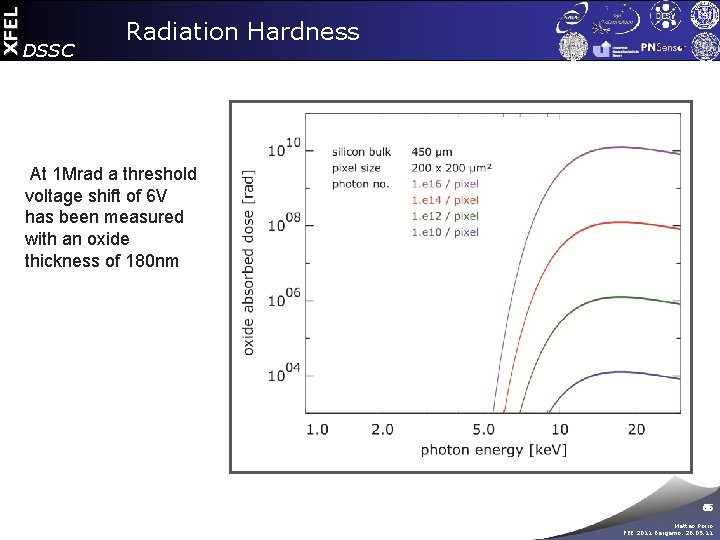
XFEL DSSC Radiation Hardness At 1 Mrad a threshold voltage shift of 6 V has been measured with an oxide thickness of 180 nm 65 Matteo Porro FEE 2011 Bergamo, 26. 05. 11

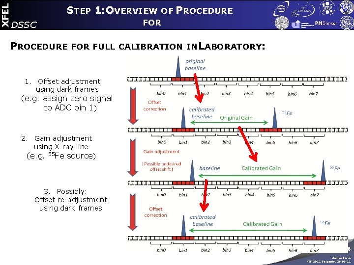
XFEL STEP 1: OVERVIEW OF PROCEDURE DSSC FOR SETTING OFFSET AND GAIN PROCEDURE FOR FULL CALIBRATION IN LABORATORY: 1. Offset adjustment using dark frames (e. g. assign zero signal to ADC bin 1) 2. Gain adjustment using X-ray line (e. g. 55 Fe source) 3. Possibly: Offset re-adjustment using dark frames 66 Matteo Porro FEE 2011 Bergamo, 26. 05. 11

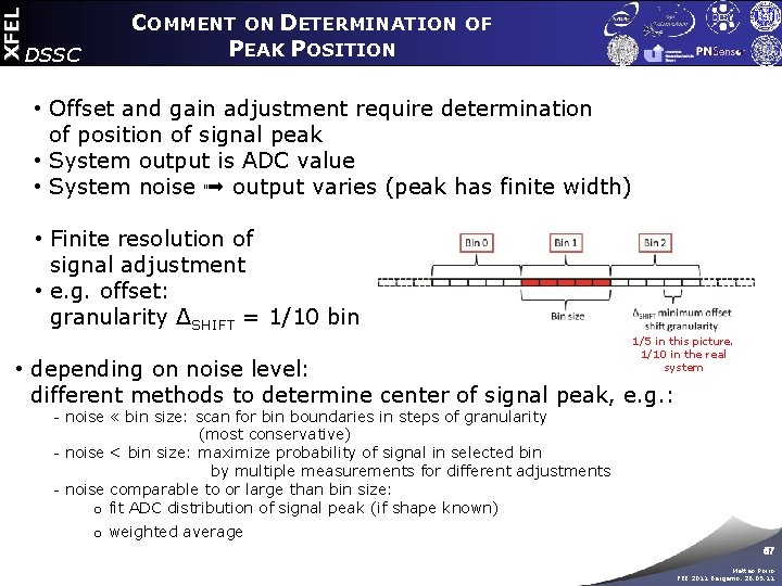
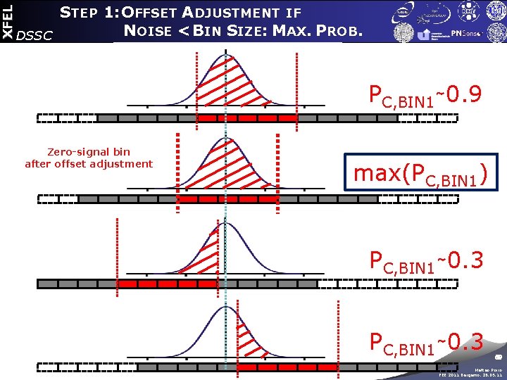
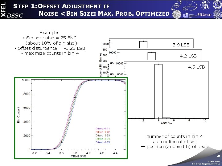
XFEL DSSC COMMENT ON DETERMINATION OF PEAK POSITION • Offset and gain adjustment require determination of position of signal peak • System output is ADC value • System noise ➟ output varies (peak has finite width) • Finite resolution of signal adjustment • e. g. offset: granularity ΔSHIFT = 1/10 bin 1/5 in this picture. 1/10 in the real system • depending on noise level: different methods to determine center of signal peak, e. g. : - noise « bin size: scan for bin boundaries in steps of granularity (most conservative) - noise < bin size: maximize probability of signal in selected bin by multiple measurements for different adjustments - noise comparable to or large than bin size: o fit ADC distribution of signal peak (if shape known) o weighted average 67 Matteo Porro FEE 2011 Bergamo, 26. 05. 11

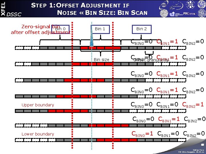
XFEL DSSC STEP 1: OFFSET ADJUSTMENT IF NOISE « BIN SIZE: BIN SCAN Zero-signal bin Bin 0 after offset adjustment Bin 1 Bin 2 CBIN 0=0 CBIN 1=1 CBIN 2=0 Bin size COffset granularity BIN 0=0 CBIN 1=1 CBIN 2=0 CBIN 0=0 CBIN 1=1 CBIN 2=0 Upper boundary CBIN 0=0 CBIN 1=0 CBIN 2=1 CBIN 0=0 CBIN 1=1 CBIN 2=0 Lower boundary CBIN 0=1 CBIN 1=0 CBIN 2=0 68 Matteo Porro FEE 2011 Bergamo, 26. 05. 11

XFEL STEP 1: OFFSET ADJUSTMENT IF NOISE < BIN SIZE: MAX. PROB. DSSC PC, BIN 1∼ 0. 9 Zero-signal bin after offset adjustment max(P PC, BIN 1 ∼ 1 ) C, BIN 1 PC, BIN 1∼ 0. 3 69 Matteo Porro FEE 2011 Bergamo, 26. 05. 11

XFEL STEP 1: OFFSET ADJUSTMENT IF NOISE < BIN SIZE: MAX. PROB. OPTIMIZED DSSC Example: • Sensor noise = 25 ENC (about 10% of bin size) • Offset disturbance = -0. 23 LSB • maximize counts in bin 4 3. 9 LSB 4. 2 LSB 4. 5 LSB number of counts in bin 4 as function of offset ➟ position (and width) of peak 70 Matteo Porro FEE 2011 Bergamo, 26. 05. 11