The readout chip for the XFEL DSSC Detector
- Slides: 21

The readout chip for the XFEL DSSC Detector: design and test Pradeep Kalavakuru, DESY for the DSSC ASIC design groups C. Fiorini 3, P. Fischer 2, K. Hansen 1, F. Erdinger 2, M. Kirchgessner 2, M. Manghisoni 4, M. Porro 5, C. Reckleben 1, J. Soldat 2 (DESY 1 , Heidelberg Univ. 2, Politecnico di Milano 3, Univ. de Bergamo 4, European XFEL Gmb. H 5) 1 FEE 2018

Outline ● Project Status ● Overview ● Characterization § ADC § Front-end ● Measurements with Sensor § Small format ASICS - X-ray sources § Focal Plane Module (FPM) - LED ● Summary 2 FEE 2018

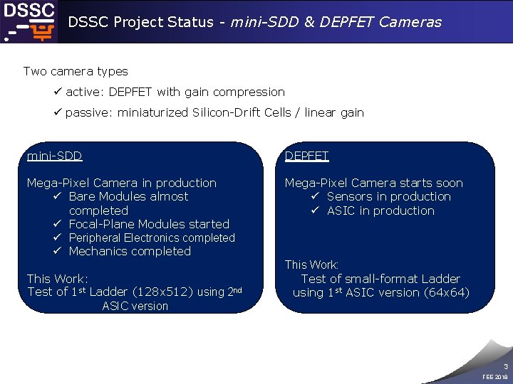
DSSC Project Status - mini-SDD & DEPFET Cameras Two camera types ü active: DEPFET with gain compression ü passive: miniaturized Silicon-Drift Cells / linear gain mini-SDD DEPFET Mega-Pixel Camera in production ü Bare Modules almost completed ü Focal-Plane Modules started ü Peripheral Electronics completed ü Mechanics completed Mega-Pixel Camera starts soon ü Sensors in production ü ASIC in production This Work: Test of 1 st Ladder (128 x 512) using 2 nd ASIC version This Work: Test of small-format Ladder using 1 st ASIC version (64 x 64) 3 FEE 2018

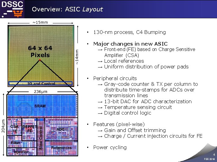
Overview: ASIC Layout • 130 -nm process, C 4 Bumping • Major changes in new ASIC → Front-end (FE) based on Charge Sensitive Amplifier (CSA) → Local references → Uniform distribution of power pads • Peripheral circuits → Gray-code counter & TX per column to distribute time-stamps for ADCs over transmission lines → 13 -bit DAC for ADC characterization → Temperature sensing circuit → Digital control logic • Features (pixel-wise) → Gain and Offset trimming → Charge / Current injection circuits for FE • Power cycling 4 FEE 2018

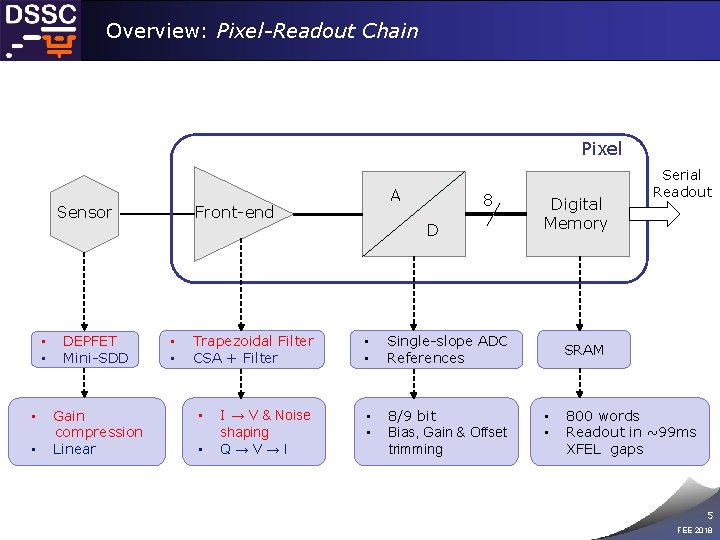
Overview: Pixel-Readout Chain Pixel Sensor • • DEPFET Mini-SDD Gain compression Linear A Front-end • • 8 D Trapezoidal Filter CSA + Filter • • Single-slope ADC References I → V & Noise shaping Q→V→I • • 8/9 bit Bias, Gain & Offset trimming • • Digital Memory Serial Readout SRAM • • 800 words Readout in ~99 ms XFEL gaps 5 FEE 2018

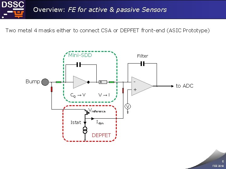
Overview: FE for active & passive Sensors Two metal 4 masks either to connect CSA or DEPFET front-end (ASIC Prototype) Mini-SDD Bump ● Filter ● ● R ● to ADC V→I Vreference ► Istat ● + CQ → V ● ● ► V Idyn DEPFET 6 FEE 2018

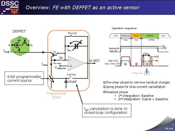
Overview: FE with DEPFET as an active sensor Operation sequence: DEPFET G -- S Reset CG CL ► ► Istat + Idyn Vreference ► ► Istat Int Ierr+dyn Vreference 4 V 2. 5 V Source (S) Gate (G) Idyn 220 ns + 12 V to ADC Clear (CL) Clear Gate (CG) 1 st 2 nd 1 Vhold 1 2 Trapezoidal Filter 8 V 3 Integration Iprog 4 -bit programmable current source 2 3 Pre-clear phase to remove residual charges Iprog phase for bias current cancellation Readout phase • 1 st Integration: Baseline • 2 nd Integration: Signal + Baseline Ierr cancelation is done in closed-loop configuration 7 FEE 2018

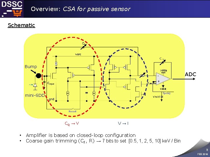
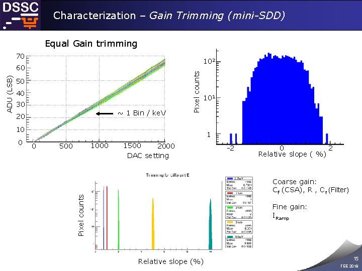
Overview: CSA for passive sensor Schematic Bump ADC Vreference mini-SDD CQ → V • • V→I Amplifier is based on closed-loop configuration Coarse gain trimming (Cf , R) → 7 bits to set [0. 5, 1, 2, 5, 10] ke. V / Bin 8 FEE 2018

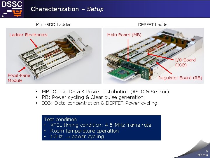
Characterization – Setup Mini-SDD Ladder Electronics DEPFET Ladder Main Board (MB) I/O Board (IOB) Focal-Pane Module Regulator Board (RB) • • • MB: Clock, Data & Power distribution (ASIC & Sensor) RB: Power cycling & Clear pulse generation IOB: Data concentration & DEPFET Power cycling Test condition • XFEL timing condition: 4. 5 -MHz frame rate • Room temperature operation • 10 Hz → power cycling 9 FEE 2018

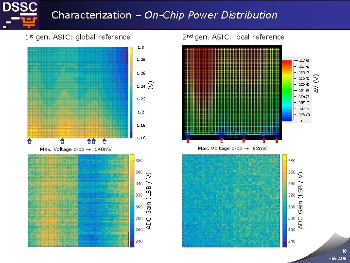
Characterization – On-Chip Power Distribution 1 st gen. ASIC: global reference 2 nd gen. ASIC: local reference 1. 3 1. 28 (V) 1. 24 ∆V (V) 1. 26 1. 22 1. 18 1. 16 2 3 3 2 4 2 3 2 Max. Voltage drop → 62 m. V Max. Voltage drop → 140 m. V ADC Gain (LSB / V) 4 ADC Gain (LSB / V) 3 10 FEE 2018

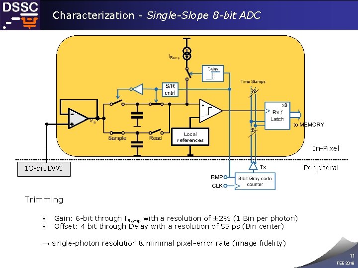
Characterization - Single-Slope 8 -bit ADC Local references In-Pixel 13 -bit DAC Peripheral Trimming • • Gain: 6 -bit through IRamp with a resolution of ± 2% (1 Bin per photon) Offset: 4 bit through Delay with a resolution of 55 ps (Bin center) → single-photon resolution & minimal pixel-error rate (image fidelity) 11 FEE 2018

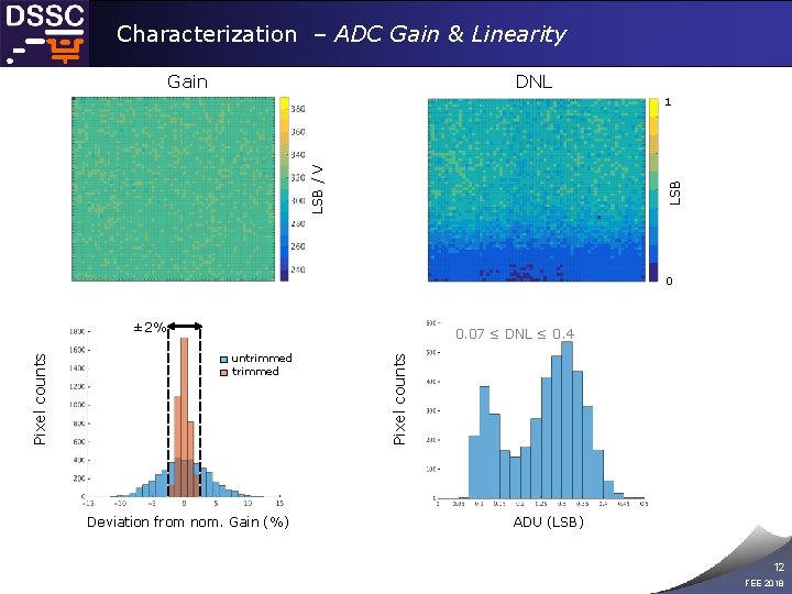
Characterization – ADC Gain & Linearity Gain DNL LSB / V 1 0 0. 07 ≤ DNL ≤ 0. 4 untrimmed Deviation from nom. Gain (%) Pixel counts ± 2% ADU (LSB) 12 FEE 2018

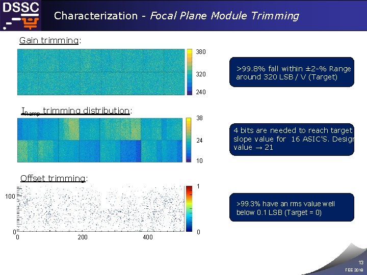
Characterization - Focal Plane Module Trimming Gain trimming: 380 320 >99. 8% fall within ± 2 -% Range around 320 LSB / V (Target) 240 IRamp trimming distribution: 38 24 4 bits are needed to reach target slope value for 16 ASIC’S. Design value → 21 10 Offset trimming: 1 100 0 0 >99. 3% have an rms value well below 0. 1 LSB (Target = 0) 200 400 0 13 FEE 2018

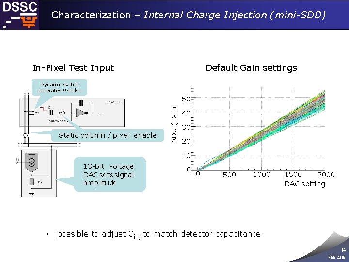
Characterization – Internal Charge Injection (mini-SDD) In-Pixel Test Input Default Gain settings Dynamic switch generates V-pulse Static column / pixel enable ADU (LSB) 50 40 30 20 10 13 -bit voltage DAC sets signal amplitude • 0 0 500 1000 1500 2000 DAC setting possible to adjust Cinj to match detector capacitance 14 FEE 2018

Characterization – Gain Trimming (mini-SDD) Equal Gain trimming 70 50 40 30 ~ 1 Bin / ke. V 20 101 10 0 1000 500 1500 2000 DAC setting -2 0 2 Relative slope ( %) Coarse gain: Cf (CSA), R , Cf (Filter) Pixel counts ADU (LSB) 60 Pixel counts 102 Fine gain: IRamp Relative slope (%) 15 FEE 2018

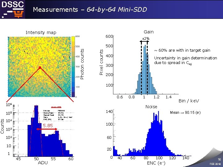
Counts Measurements – 64 -by-64 Mini-SDD Intensity map Gain 600 ± 2% Pixel counts Photon counts 500 ~ 60% are with in target gain 400 Uncertainty in gain determination due to spread in Cinj 300 200 100 0. 6 106 0. 8 105 104 780000 49. 91 55. 76 1. 01 Bin / ke. V 97. 2 e - 1. 4 Bin / ke. V 140 Mean → 90. 15 (e-) 100 5. 85 103 1. 2 Noise Pixel 1950 Entries Noise Peak Signal Peak Gain ENC (fit) 1 60 102 10 20 1 45 50 ADU 55 60 0 40 60 80 100 ENC (e-) 120 140 16 FEE 2018

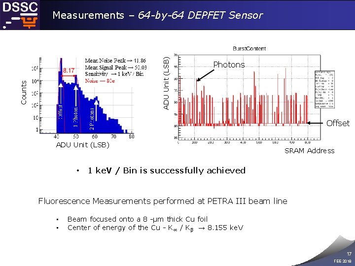
Counts ADU Unit (LSB) Measurements – 64 -by-64 DEPFET Sensor Photons Offset ADU Unit (LSB) • SRAM Address 1 ke. V / Bin is successfully achieved Fluorescence Measurements performed at PETRA III beam line • • Beam focused onto a 8 -µm thick Cu foil Center of energy of the Cu - K∝ / Kβ → 8. 155 ke. V 17 FEE 2018

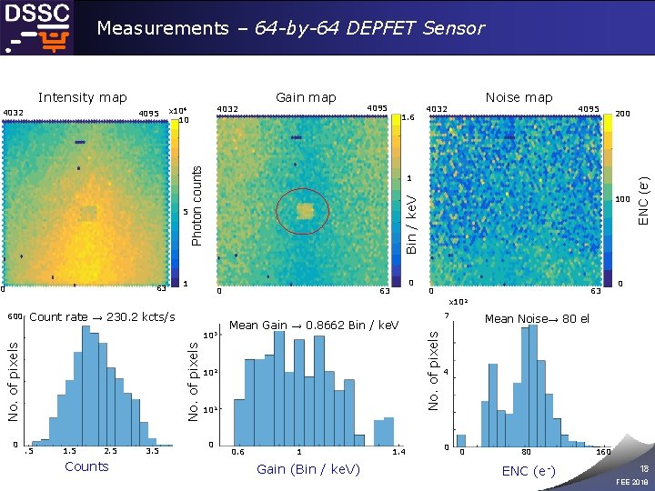
Measurements – 64 -by-64 DEPFET Sensor 63 Gain map 4095 1. 6 Noise map 4032 4095 200 1 100 Bin / ke. V 5 0 4032 x 104 10 Photon counts 4095 1 0 63 0 ENC (e-) Intensity map 4032 0 x 102 Count rate → 230. 2 kcts/s 0 No. of pixels 103 . 5 1. 5 2. 5 Counts 3. 5 102 101 0 7 Mean Gain → 0. 8662 Bin / ke. V No. of pixels 600 0. 6 1 Gain (Bin / ke. V) 1. 4 Mean Noise→ 80 el 4 0 0 80 ENC (e-) 160 18 FEE 2018

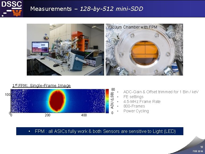
Measurements – 128 -by-512 mini-SDD Vacuum Chamber with FPM 1 st FPM: Single-Frame Image 80 • • • 0 ADU (LSB) 100 0 0 200 • 400 ADC-Gain & Offset trimmed for 1 Bin / ke. V FE settings 4. 5 -MHz Frame Rate 800 -Frames Power Cycling FPM : all ASICs fully work & both Sensors are sensitive to Light (LED) 19 FEE 2018

Summary • We presented the successful operation of the full detector chain with DEPFET and mini-SDD sensors. • The 1 st mini-SDD Focal Plane Module of the Mega-pixel camera was successfully tested in power cycling mode at XFEL timing condition. • Gain & Offset trimming as well as noise performance fulfills the design requirements for single-photon resolution: » Gain Trimming → 99. 9 % falls in ± 2% range of nominal gain 320 LSB / V at 1 ke. V » Offset Trimming → 99. 3 % have standard deviation of ‹ 0. 1 LSB » mini-SDD Noise → 90 e- at room temperature » DEPFET Noise → 80 e- at room temperature 20 FEE 2018

Thank You 21 FEE 2018