DEPFET Readout Electronics Ivan Peric Jochen Kinzel Christian







- Slides: 77

DEPFET Readout Electronics Ivan Peric, Jochen Kinzel, Christian Kreidl, Peter Fischer University of Heidelberg 1

Introduction 2

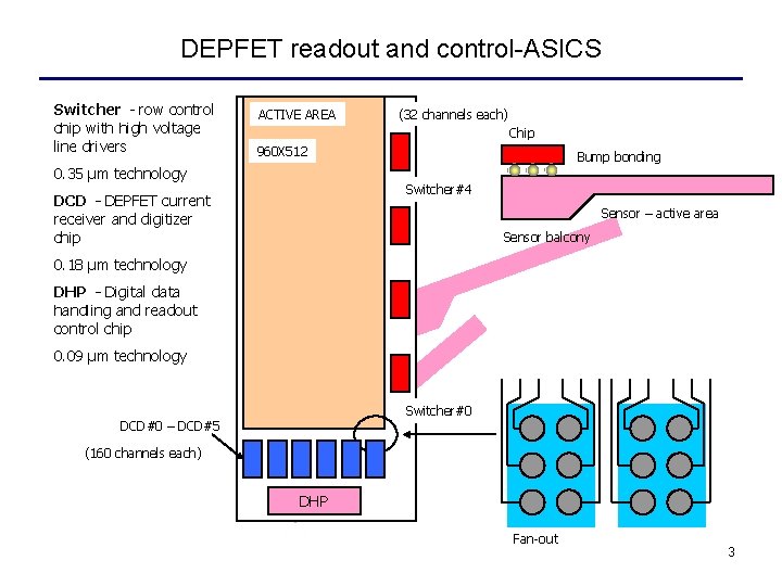
DEPFET readout and control-ASICS Switcher – row control chip with high voltage line drivers ACTIVE AREA (32 channels each) Chip 960 X 512 0. 35 μm technology Bump bonding Switcher#4 DCD – DEPFET current receiver and digitizer chip Sensor – active area Sensor balcony 0. 18 μm technology DHP – Digital data handling and readout control chip 0. 09 μm technology Switcher#0 DCD#0 – DCD#5 (160 channels each) DHP Fan-out 3

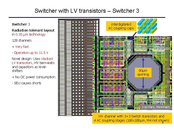
Switcher with LV transistors – Switcher 3 Radiation tolerant layout in 0. 35 μm technology interdigitated AC coupling caps 128 channels + Very fast - Operation up to 11. 5 V Novel design: Uses stacked LV transistors, HV twin-wells and capacitors as levelshifters + No DC power consumption 80µm opening - SEU causes shorts Ivan Peric, Mannheim HV channel with 3+3 Switch transistors and 4 AC coupling stages (180 x 180µm, M 4 not shown) 4

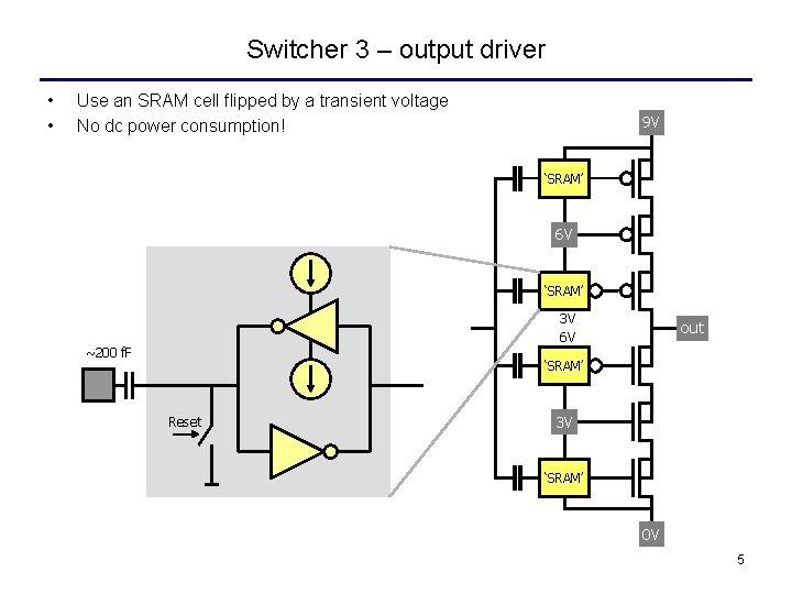
Switcher 3 – output driver • • Use an SRAM cell flipped by a transient voltage No dc power consumption! 9 V ‘SRAM’ 6 V ‘SRAM’ 3 V 6 V ~200 f. F out ‘SRAM’ Reset 3 V ‘SRAM’ 0 V 5

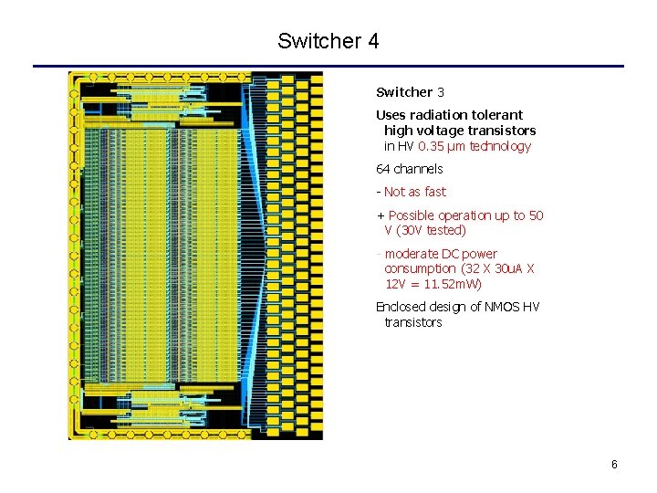
Switcher 4 Switcher 3 Uses radiation tolerant high voltage transistors in HV 0. 35 μm technology 64 channels - Not as fast + Possible operation up to 50 V (30 V tested) - moderate DC power consumption (32 X 30 u. A X 12 V = 11. 52 m. W) Enclosed design of NMOS HV transistors 6

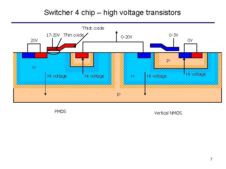
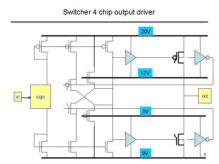
Switcher 4 chip – high voltage transistors Thick oxide 17 -20 V Thin oxide 0 -3 V 0 -20 V 0 V pn. Hi voltage n- Hi voltage p- PMOS Vertical NMOS 7

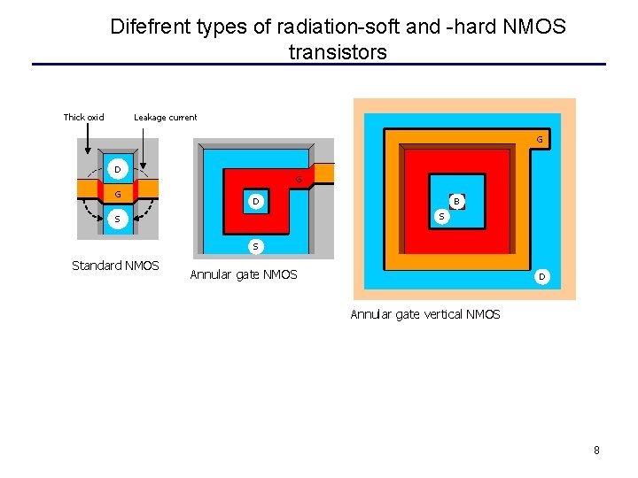
Difefrent types of radiation-soft and -hard NMOS transistors Thick oxid Leakage current G D G G D B S Standard NMOS Annular gate NMOS D Annular gate vertical NMOS 8

Switcher 4 chip output driver 20 V 17 V in out logic 3 V 0 V 9

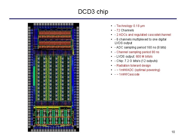
DCD 3 chip • • • - Technology 0. 18 μm - 72 Channels - 2 ADCs and regulated cascode/channel - 6 channels multiplexed to one digital LVDS output - ADC sampling period 160 ns (8 bits) - Channel sampling period 80 ns - LVDS output: 600 M bits/s - Chip: 7. 2 G bits/s (12 outputs) - Radiation tolerant design - ~ 1 m. W/ADC (optimal powering) - ~ 1 m. W/Cascode 10

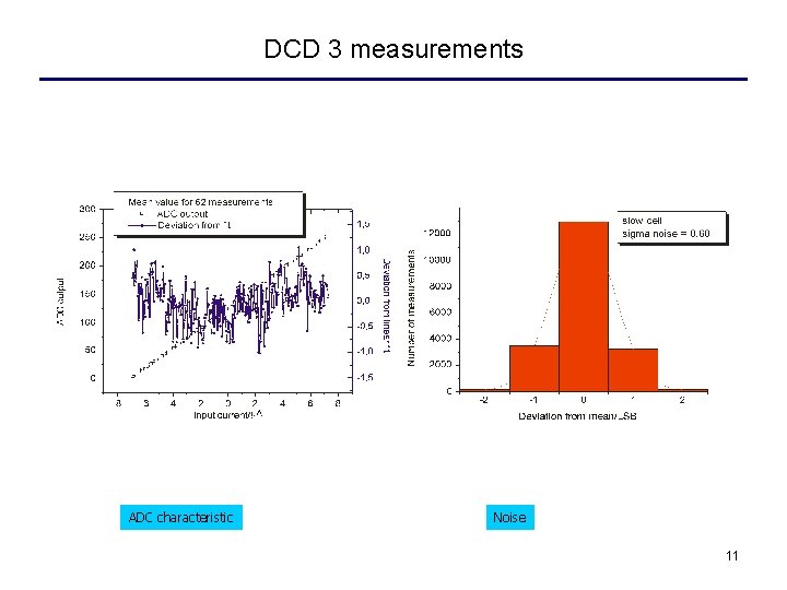
DCD 3 measurements ADC characteristic Noise 11

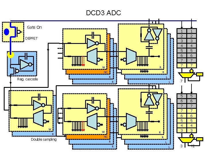
DCD 3 ADC Gate On 1 2 3 4 5 6 7 7 DEPFET W R NC R R Reg. cascode L R W R Double sampling 1 2 3 4 5 6 7 7 W L R NC 7 5 6 7 7 6 5 4 3 3 12 R R L

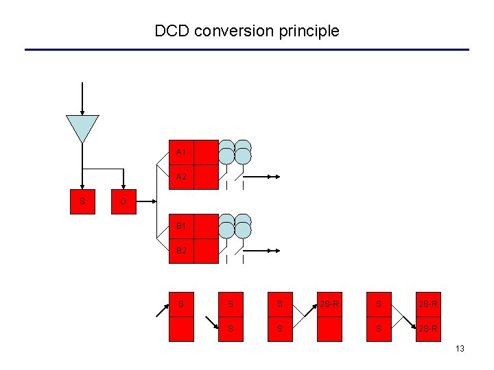
DCD conversion principle A 1 A 2 S O B 1 B 2 S S S 2 S-R 13

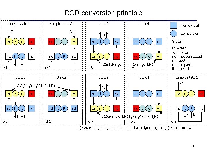
DCD conversion principle sample state 1 sample state 2 S wr S r r 1. nc state 3 lt lt 3. nc nc 2. 1. nc nc 4. 3. ck 1 c c h 0 wr lt memory cell l 0 comparator rd lt lt rd 2. lt lt nc wr r 4. ck 2 state 1 rd state 4 2(S-h 0 R+l 0 R) ck 3 state 2 nc r nc h 2 c wr 2(S-h 0 R+l 0 R) ck 4 state 3 2(2(S-h 0 R+l 0 R)-h 1 R+l 1 R) c state 4 States: rd – read wr – write nc – not connected r – reset c – compare lt - latched sample state 1 S‘ l 2 wr r r nc nc c c wr rd lt lt rd wr r r nc nc c c wr nc lt lt nc h 1 ck 5 l 1 ck 6 ck 7 2(2(2(S-h 0 R+l 0 R)-h 1 R+l 1 R)–h 2 R+l 2 R) ck 8 h 3 l 3 ck 9 2(2(S - h 0 R + l 0 R) - h 1 R + l 1 R) – h 2 R + l 2 R) – h 3 R + l 3 R) = Res 14

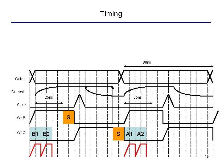
Timing 80 ns Gate Current 25 ns Clear S Wr O B 1 B 2 S A 1 A 2 15

Channel geometry Current receiver 1000 u. A Power line Logic Data compression Pad 110 um 180 um 16

DCD Improvements 17

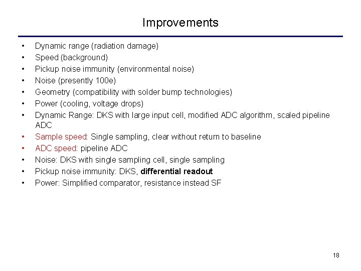
Improvements • • • Dynamic range (radiation damage) Speed (background) Pickup noise immunity (environmental noise) Noise (presently 100 e) Geometry (compatibility with solder bump technologies) Power (cooling, voltage drops) Dynamic Range: DKS with large input cell, modified ADC algorithm, scaled pipeline ADC Sample speed: Single sampling, clear without return to baseline ADC speed: pipeline ADC Noise: DKS with single sampling cell, single sampling Pickup noise immunity: DKS, differential readout Power: Simplified comparator, resistance instead SF 18

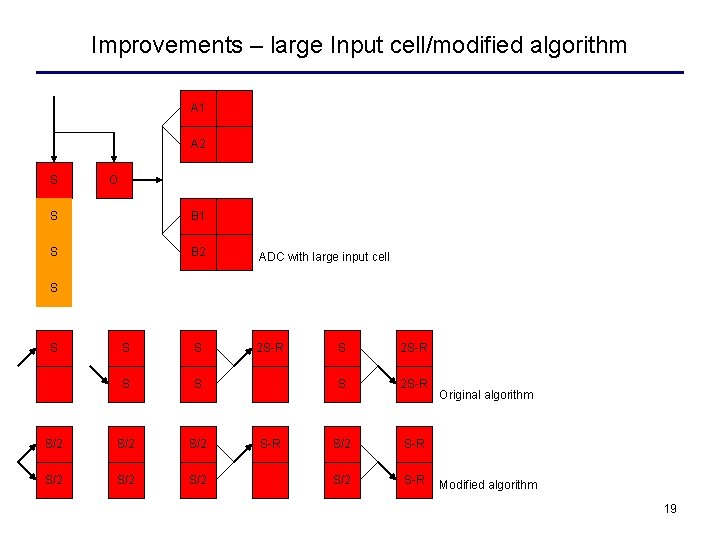
Improvements – large Input cell/modified algorithm A 1 A 2 S O S B 1 S B 2 ADC with large input cell S S 2 S-R S S S/2 S/2 S/2 S S S-R S 2 S-R S/2 S-R Original algorithm Modified algorithm 19

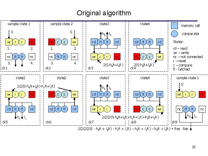
Original algorithm sample state 1 sample state 2 S wr S r r 1. nc state 3 lt lt 3. nc nc 2. 1. nc nc 4. 3. ck 1 c c h 0 wr lt memory cell l 0 comparator rd lt lt rd 2. lt lt nc wr r 4. ck 2 state 1 rd state 4 2(S-h 0 R+l 0 R) ck 3 state 2 nc r nc h 2 c wr 2(S-h 0 R+l 0 R) ck 4 state 3 2(2(S-h 0 R+l 0 R)-h 1 R+l 1 R) c state 4 States: rd – read wr – write nc – not connected r – reset c – compare lt - latched sample state 1 S‘ l 2 wr r r nc nc c c wr rd lt lt rd wr r r nc nc c c wr nc lt lt nc h 1 ck 5 l 1 ck 6 ck 7 2(2(2(S-h 0 R+l 0 R)-h 1 R+l 1 R)–h 2 R+l 2 R) ck 8 h 3 l 3 ck 9 2(2(S - h 0 R + l 0 R) - h 1 R + l 1 R) – h 2 R + l 2 R) – h 3 R + l 3 R) = Res 20

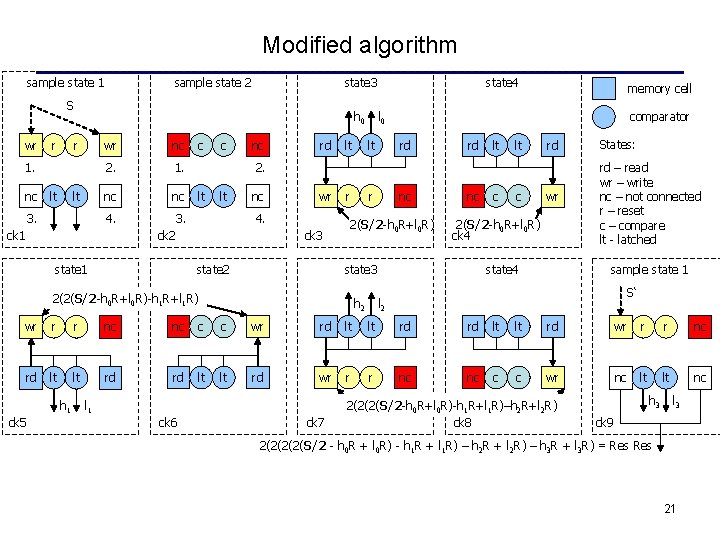
Modified algorithm sample state 1 sample state 2 state 3 S wr r h 0 r 1. nc lt lt 3. wr nc 2. 1. nc nc 4. 3. ck 1 c c nc lt memory cell l 0 comparator rd lt lt rd 2. lt lt nc wr 4. ck 2 state 1 rd state 4 ck 3 state 2 r nc r 2(S/2 -h 0 R+l 0 R) nc h 2 c wr 2(S/2 -h 0 R+l 0 R) ck 4 state 3 2(2(S/2 -h 0 R+l 0 R)-h 1 R+l 1 R) c state 4 States: rd – read wr – write nc – not connected r – reset c – compare lt - latched sample state 1 S‘ l 2 wr r r nc nc c c wr rd lt lt rd wr r r nc nc c c wr nc lt lt nc h 1 ck 5 l 1 ck 6 ck 7 2(2(2(S/2 -h 0 R+l 0 R)-h 1 R+l 1 R)–h 2 R+l 2 R) ck 8 h 3 l 3 ck 9 2(2(S/2 - h 0 R + l 0 R) - h 1 R + l 1 R) – h 2 R + l 2 R) – h 3 R + l 3 R) = Res 21

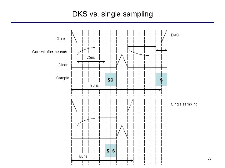
DKS vs. single sampling DKS Gate Current after cascode 25 ns Clear Sample so s 80 ns Single sampling s s 55 ns 22

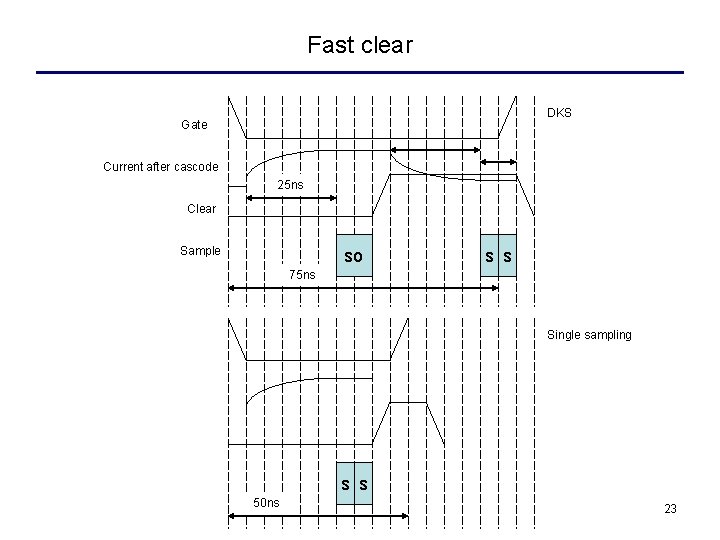
Fast clear DKS Gate Current after cascode 25 ns Clear Sample so s s 75 ns Single sampling s s 50 ns 23

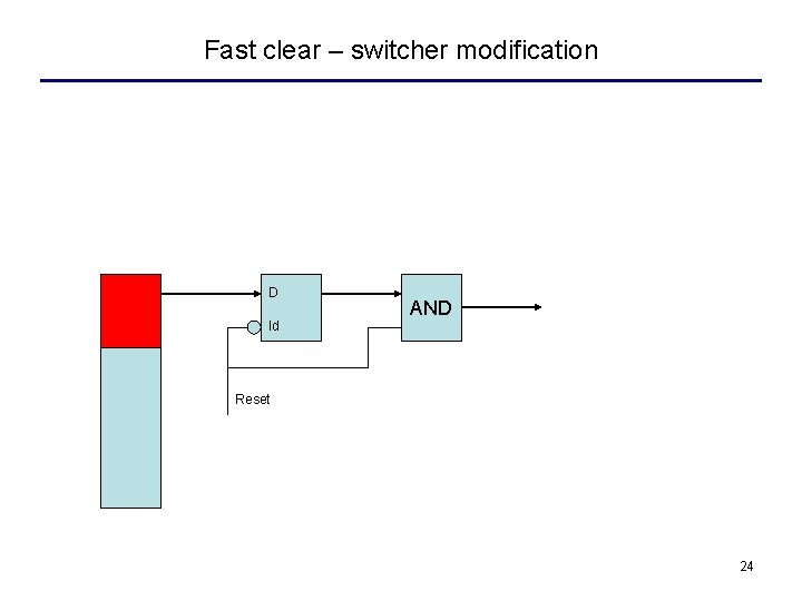
Fast clear – switcher modification D ld AND Reset 24

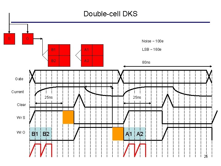
Double-cell DKS S O Noise ~ 100 e B 1 A 1 LSB ~ 160 e B 2 A 2 80 ns Gate Current 25 ns Clear Wr S Wr O B 1 B 2 A 1 A 2 25

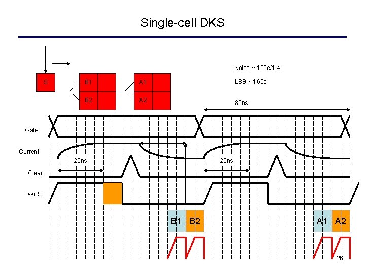
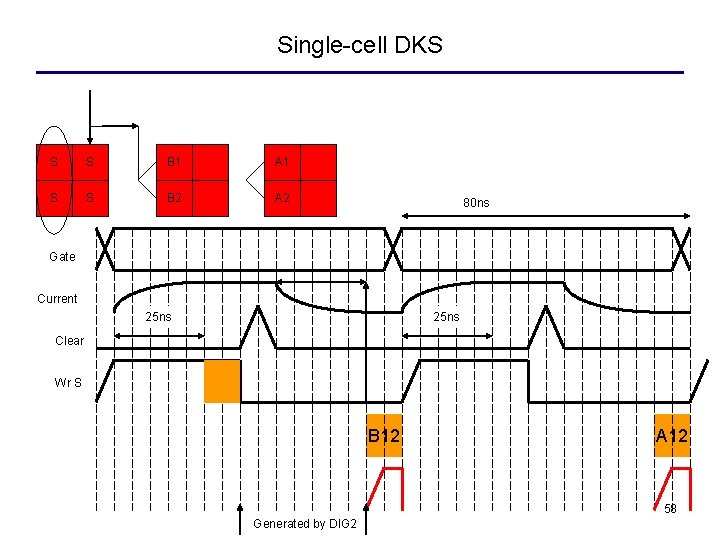
Single-cell DKS Noise ~ 100 e/1. 41 S B 1 A 1 LSB ~ 160 e B 2 A 2 80 ns Gate Current 25 ns Clear Wr S B 1 B 2 A 1 A 2 26

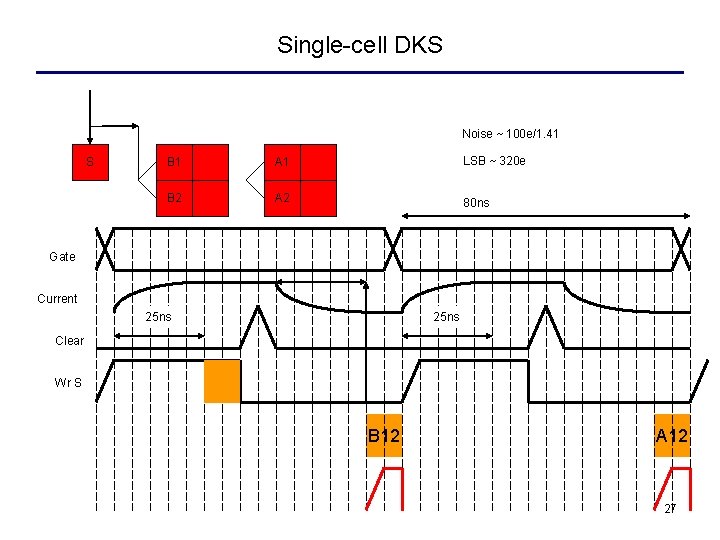
Single-cell DKS Noise ~ 100 e/1. 41 S B 1 A 1 LSB ~ 320 e B 2 A 2 80 ns Gate Current 25 ns Clear Wr S B 12 A 12 27

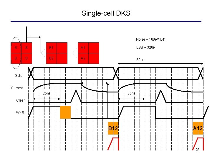
Single-cell DKS Noise ~ 100 e. X 1. 41 S S B 1 A 1 LSB ~ 320 e S S B 2 A 2 80 ns Gate Current 25 ns Clear Wr S B 12 A 12 28

ADC Cell Lo Hi C 1 Rd R Logic Amp. Low Wr. B* Sub Rd. B C 2 Add Amp. Low Wr. B 24 μA 6 X 2 μA Rd 12 μA Wr Vbias Ref. In 24 μA To Comp In? Or use Th instead Gate 29

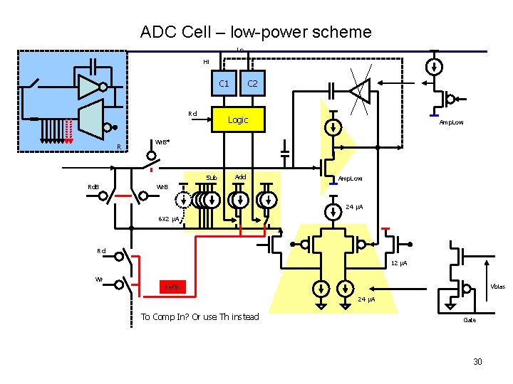
ADC Cell – low-power scheme Lo Hi C 1 Rd R Logic Amp. Low Wr. B* Sub Rd. B C 2 Add Amp. Low Wr. B 24 μA 6 X 2 μA Rd 12 μA Wr Vbias Ref. In 24 μA To Comp In? Or use Th instead Gate 30

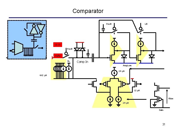
Comparator Res. B LB Or th Res. B L Ref. In Th Comp In Amp. Low 24 μA 6 X 2 μA 12 μA Vbias 24 μA Gate 31

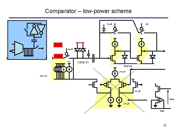
Comparator – low-power scheme Res. B LB Or th Res. B L Ref. In Th Comp In Amp. Low 24 μA 6 X 2 μA 12 μA Vbias 24 μA Gate 32

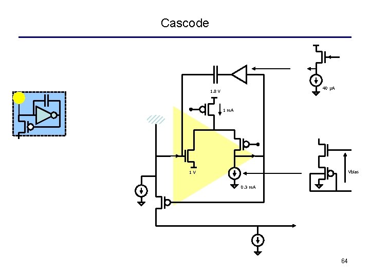
Cascode 40 μA 1. 8 V 1 m. A Vbias 1 V 0. 3 m. A 33

Novel readout concept - pixel difference readout 34

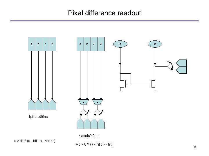
Pixel difference readout a b c d a b - 4 pixels/80 ns 4 pixels/40 ns a > th ? (a - hit : a - not hit) a-b > 0 ? (a - hit : b - hit) 35

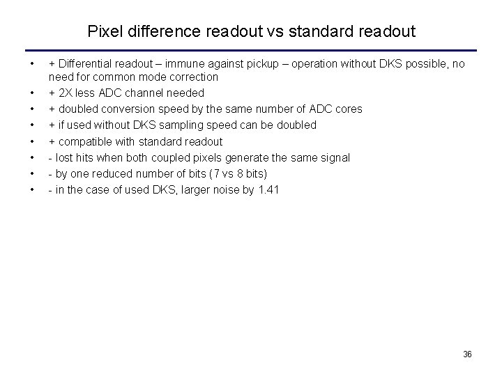
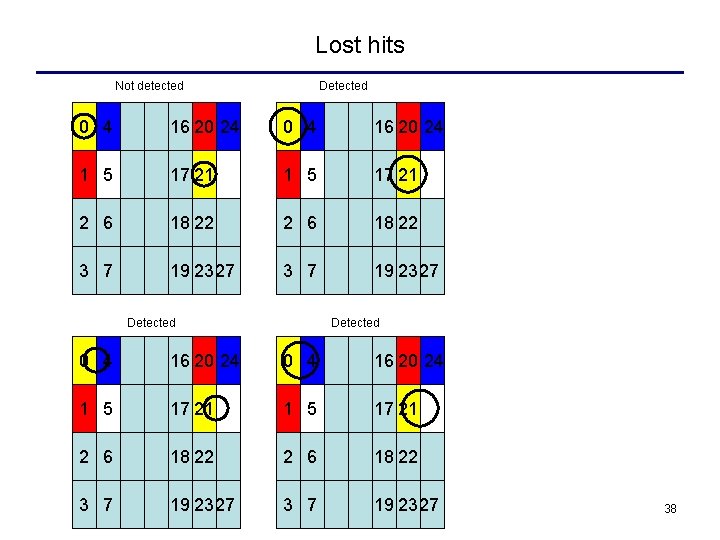
Pixel difference readout vs standard readout • • + Differential readout – immune against pickup – operation without DKS possible, no need for common mode correction + 2 X less ADC channel needed + doubled conversion speed by the same number of ADC cores + if used without DKS sampling speed can be doubled + compatible with standard readout - lost hits when both coupled pixels generate the same signal - by one reduced number of bits (7 vs 8 bits) - in the case of used DKS, larger noise by 1. 41 36

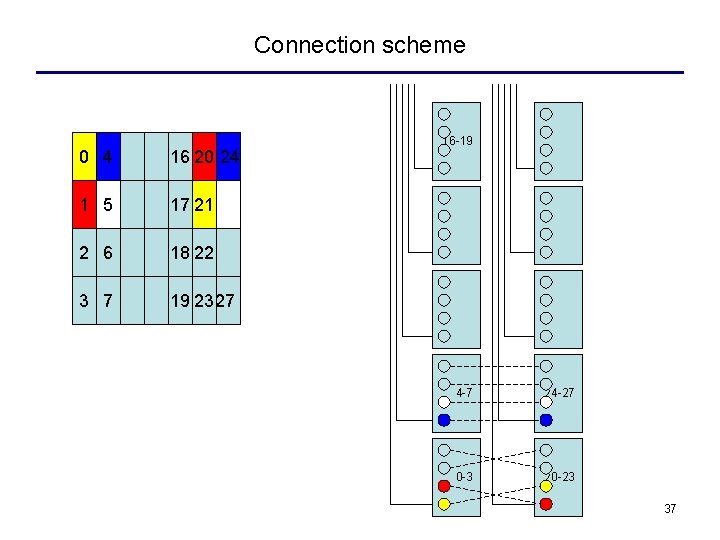
Connection scheme 0 4 16 20 24 1 5 17 21 2 6 18 22 3 7 19 23 27 16 -19 4 -7 24 -27 0 -3 20 -23 37

Lost hits Not detected Detected 0 4 16 20 24 1 5 17 21 2 6 18 22 3 7 19 23 27 38

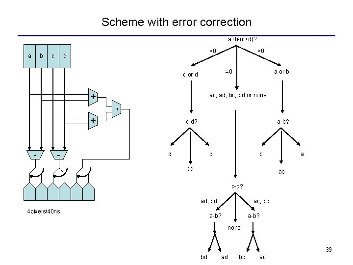
Scheme with error correction a+b-(c+d)? a b c <0 d >0 =0 c or d a or b + - + ac, ad, bc, bd or none - - c-d? a-b? d c b cd a ab c-d? ad, bd 4 pixels/40 ns ac, bc a-b? none 39 bd ad bc ac

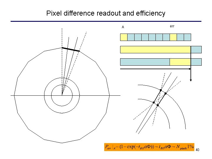
Pixel difference readout and efficiency A err 40

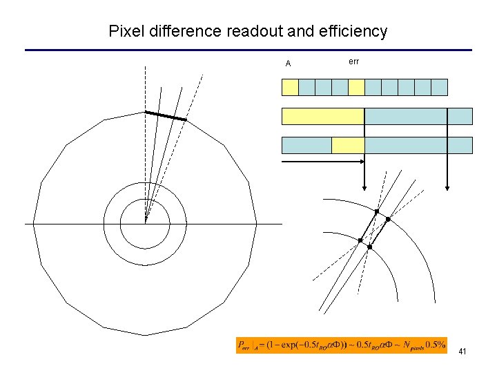
Pixel difference readout and efficiency A err 41

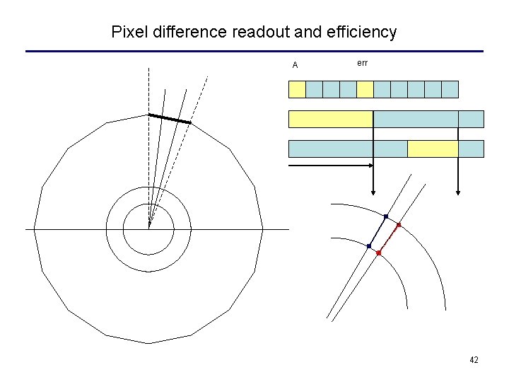
Pixel difference readout and efficiency A err 42

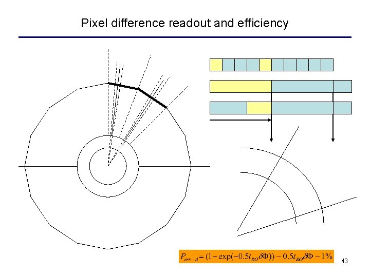
Pixel difference readout and efficiency 43

DCD channel geometry 44

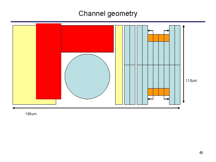
Channel geometry Current receiver Power line Logic Data compression Pad 110 um 180 um 45

Channel geometry 110 um 185 um 46

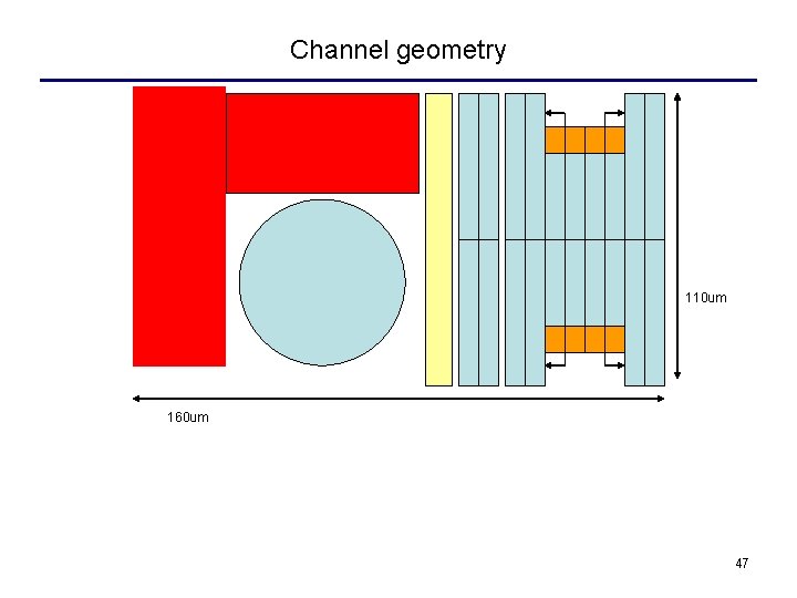
Channel geometry 110 um 160 um 47

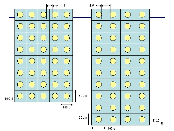
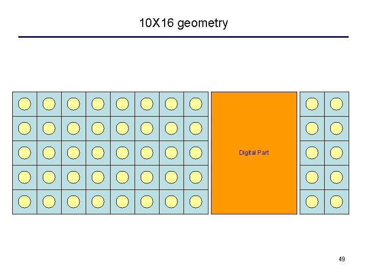
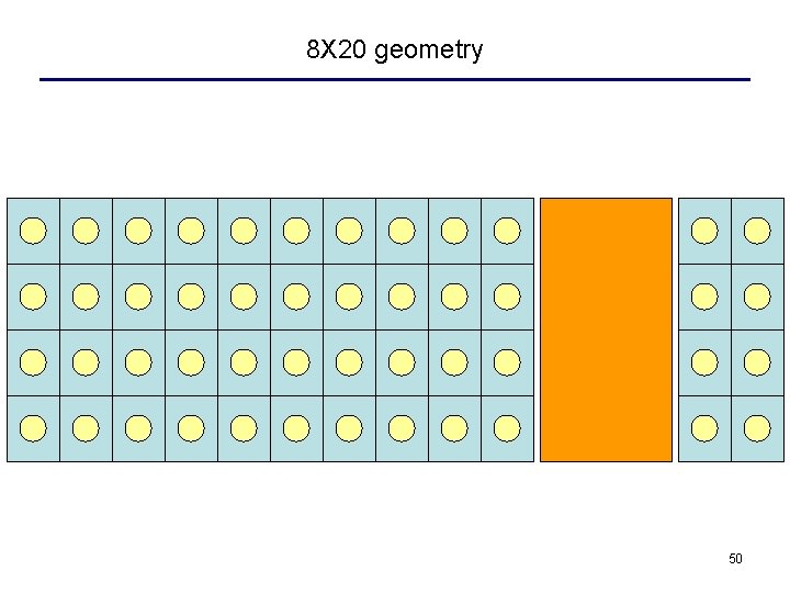
1: 1. 5 150 um 10 X 16 150 um 8 X 20 190 um 48

10 X 16 geometry Digital Part 49

8 X 20 geometry 50

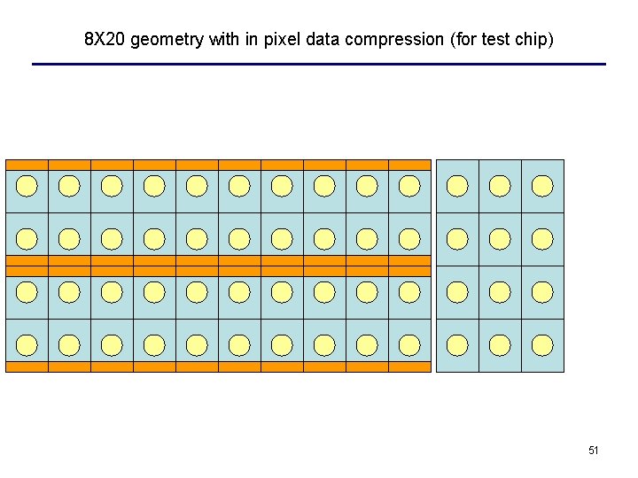
8 X 20 geometry with in pixel data compression (for test chip) 51

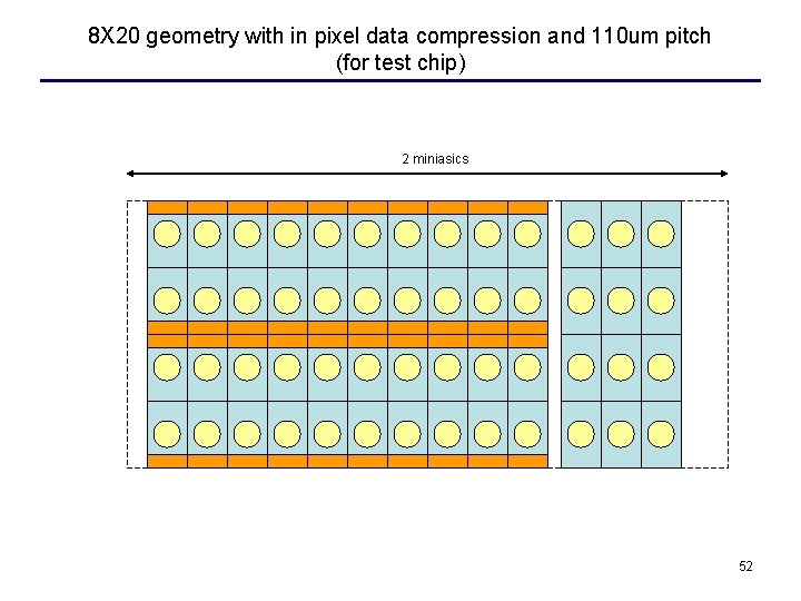
8 X 20 geometry with in pixel data compression and 110 um pitch (for test chip) 2 miniasics 52

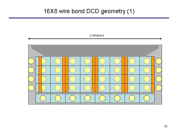
16 X 8 wire bond DCD geometry (1) 2 miniasics 53

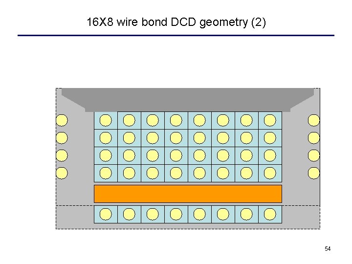
16 X 8 wire bond DCD geometry (2) 54

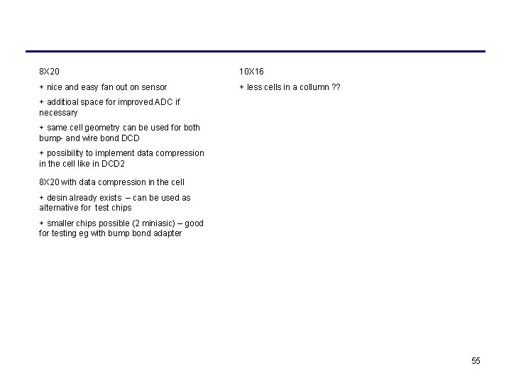
8 X 20 10 X 16 + nice and easy fan out on sensor + less cells in a collumn ? ? + additioal space for improved ADC if necessary + same cell geometry can be used for both bump- and wire bond DCD + possibility to implement data compression in the cell like in DCD 2 8 X 20 with data compression in the cell + desin already exists – can be used as alternative for test chips + smaller chips possible (2 miniasic) – good for testing eg with bump bond adapter 55

Some ideas on test system – to be done with Bonn 56

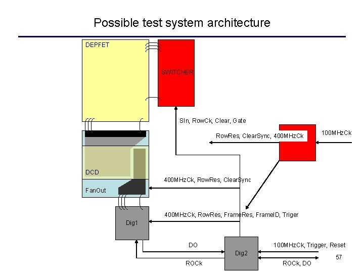
Possible test system architecture DEPFET SWITCHER SIn, Row. Ck, Clear, Gate Row. Res, Clear. Sync, 400 MHz. Ck 100 MHz. Ck DCD 400 MHz. Ck, Row. Res, Clear. Sync Fan. Out 400 MHz. Ck, Row. Res, Frame. ID, Triger Dig 1 DO 100 MHz. Ck, Trigger, Reset Dig 2 ROCk, DO 57

Single-cell DKS S S B 1 A 1 S S B 2 A 2 80 ns Gate Current 25 ns Clear Wr S B 12 A 12 58 Generated by DIG 2

Power Current receiver 1000 u. A Power line Logic Data compression Pad 110 um 180 um 84 u. A 72 u. A 59

ADC Cell Lo Hi C 1 Rd R Logic Amp. Low Wr. B* Sub Rd. B C 2 Add Amp. Low Wr. B 24 μA 6 X 2 μA Rd 12 μA Wr Vbias Ref. In 24 μA To Comp In? Or use Th instead Gate 60

ADC Cell Lo Hi C 1 Rd R Logic Amp. Low Wr. B* Sub Rd. B C 2 Add Amp. Low Wr. B 24 μA 6 X 2 μA Rd 12 μA Wr Vbias Ref. In 24 μA To Comp In? Or use Th instead Gate 61

Comparator Res. B LB Or th Res. B L Ref. In Th Comp In Amp. Low 24 μA 6 X 2 μA 12 μA Vbias 24 μA Gate 62

Comparator Res. B LB Or th Res. B L Ref. In Th Comp In Amp. Low 24 μA 6 X 2 μA 12 μA Vbias 24 μA Gate 63

Cascode 40 μA 1. 8 V 1 m. A Vbias 1 V 0. 3 m. A 64

Powering of the DCD 65

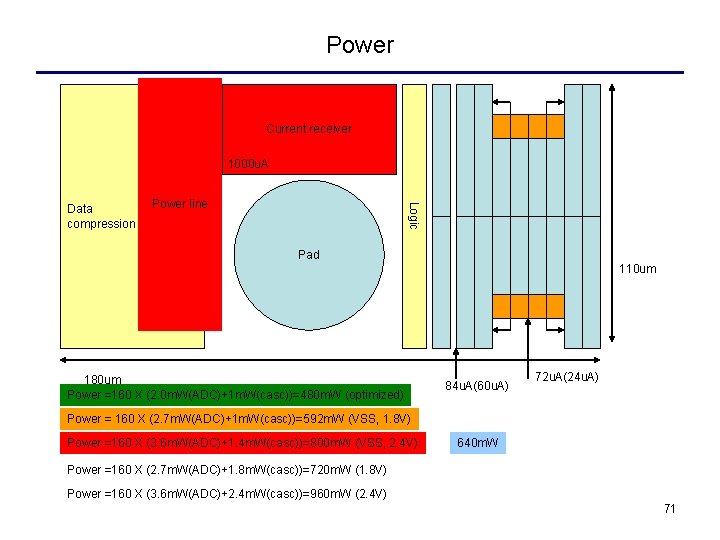
Power Current receiver 1000 u. A Power line Logic Data compression Pad 110 um 180 um 84 u. A(60 u. A) 72 u. A(24 u. A) 2 XADC: 72 u. AX 8+84 u. AX 12=1584 u. A Pixel: 1. 5 m. A + 1 m. A Chip: 2. 5 m. AX 160=400 m. A 66

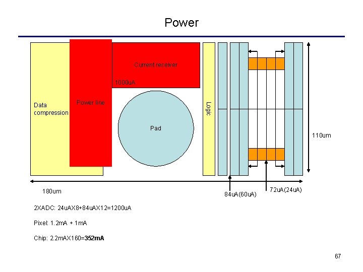
Power Current receiver 1000 u. A Power line Logic Data compression Pad 110 um 180 um 84 u. A(60 u. A) 72 u. A(24 u. A) 2 XADC: 24 u. AX 8+84 u. AX 12=1200 u. A Pixel: 1. 2 m. A + 1 m. A Chip: 2. 2 m. AX 160=352 m. A 67

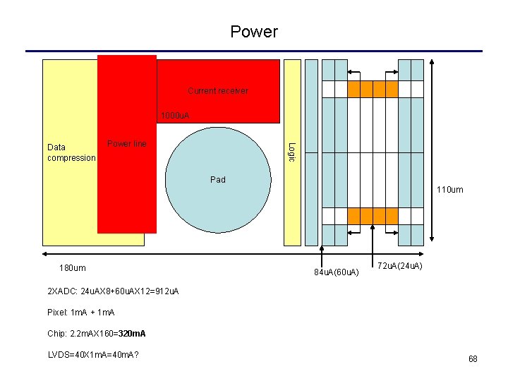
Power Current receiver 1000 u. A Power line Logic Data compression Pad 110 um 180 um 84 u. A(60 u. A) 72 u. A(24 u. A) 2 XADC: 24 u. AX 8+60 u. AX 12=912 u. A Pixel: 1 m. A + 1 m. A Chip: 2. 2 m. AX 160=320 m. A LVDS=40 X 1 m. A=40 m. A? 68

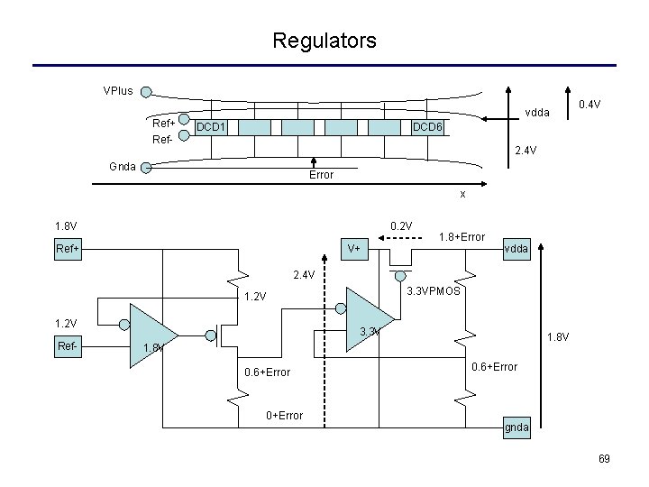
Regulators VPlus Ref+ Ref- vdda DCD 1 0. 4 V DCD 6 2. 4 V Gnda Error x 1. 8 V 0. 2 V Ref+ V+ 1. 8+Error vdda 2. 4 V 3. 3 VPMOS 1. 2 V Ref- 3. 3 V 1. 8 V 0. 6+Error gnda 69

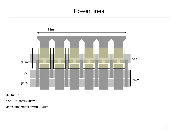
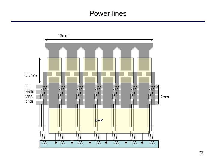
Power lines 12 mm 3. 5 mm VSS V+ gnda 2 mm 320 m. AX 6 1 AX 0. 21 Ohm=210 m. V 35 m. Ohm. X 6 mm/1 mm=0. 21 Ohm 70

Power Current receiver 1000 u. A Power line Logic Data compression Pad 110 um 180 um Power =160 X (2. 0 m. W(ADC)+1 m. W(casc))=480 m. W (optimized) 84 u. A(60 u. A) 72 u. A(24 u. A) Power = 160 X (2. 7 m. W(ADC)+1 m. W(casc))=592 m. W (VSS, 1. 8 V) Power =160 X (3. 6 m. W(ADC)+1. 4 m. W(casc))=800 m. W (VSS, 2. 4 V) 640 m. W Power =160 X (2. 7 m. W(ADC)+1. 8 m. W(casc))=720 m. W (1. 8 V) Power =160 X (3. 6 m. W(ADC)+2. 4 m. W(casc))=960 m. W (2. 4 V) 71

Power lines 12 mm 3. 5 mm V+ Ref. In VSS gnda 2 mm DHP 72

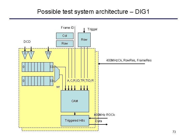
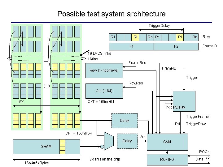
Possible test system architecture – DIG 1 Frame ID Trigger Col Row DCD 0 1 Row 15 400 MHz. Ck, Row. Res, Frame. Res 0 63 A, C, R, ID, TR, TID, R wr CAM 400 MHz ROCk Triggered Hits Data 73

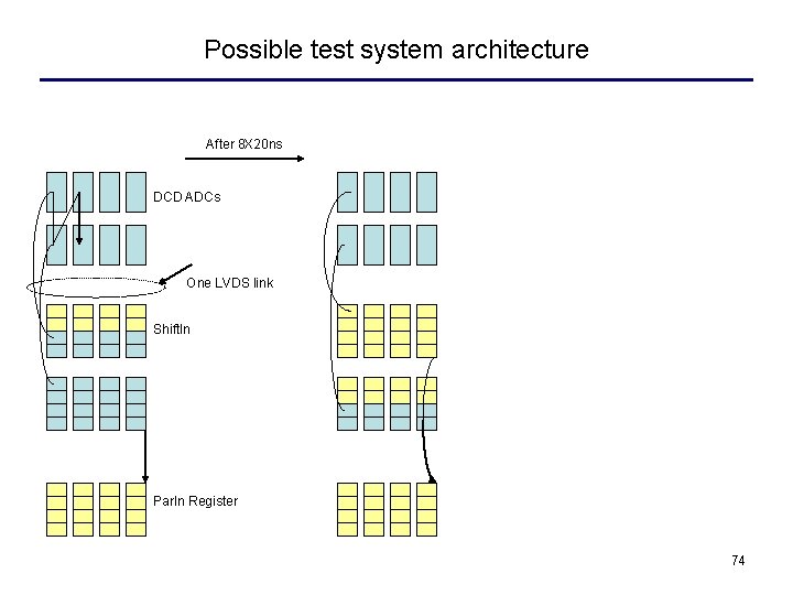
Possible test system architecture After 8 X 20 ns DCD ADCs One LVDS link Shift. In Par. In Register 74

Possible test system architecture Trigger. Delay R 1 Ri Rn R 1 Ri F 1 16 LVDS links 160 ns Rn Row Frame. ID F 2 Frame. Res Frame. ID Row (1 -noofrows) Trigger Row. Res (…) Col (1 -64) 16 X Ck. T = 160 ns/64 Trigger. Delay Trigger. Frame Delay Ck. T = 160 ns/64 Delay Rd Trigger. Row Wr CAM SRAM 16 X 4=64 Bytes 2 X this on the chip ROFIFO ROCk Data 75

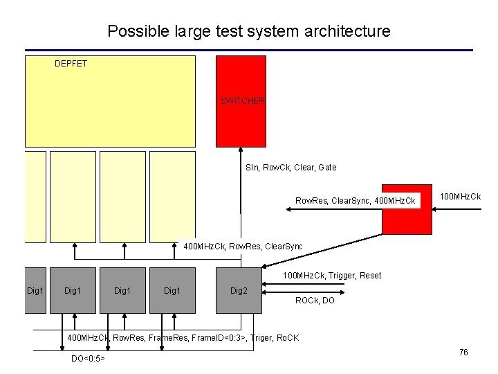
Possible large test system architecture DEPFET SWITCHER SIn, Row. Ck, Clear, Gate Row. Res, Clear. Sync, 400 MHz. Ck 100 MHz. Ck 400 MHz. Ck, Row. Res, Clear. Sync 100 MHz. Ck, Trigger, Reset Dig 1 Dig 2 ROCk, DO 400 MHz. Ck, Row. Res, Frame. ID<0: 3>, Triger, Ro. CK DO<0: 5> 76

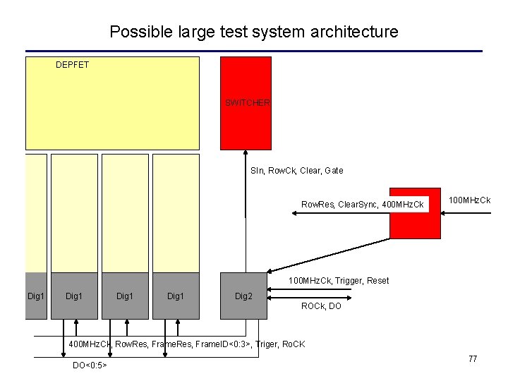
Possible large test system architecture DEPFET SWITCHER SIn, Row. Ck, Clear, Gate Row. Res, Clear. Sync, 400 MHz. Ck 100 MHz. Ck, Trigger, Reset Dig 1 Dig 2 ROCk, DO 400 MHz. Ck, Row. Res, Frame. ID<0: 3>, Triger, Ro. CK DO<0: 5> 77