DEPFET detectors for future colliders Activities at IFIC

- Slides: 35

DEPFET detectors for future colliders. Activities at IFIC, Valencia Terceras Jornadas sobre la Participación Española en los Futuros Aceleradores Lineales de Partículas Universitat de Barcelona Carlos Mariñas, IFIC, CSIC-UVEG C. Mariñas, IFIC, CSIC-UVEG

DEPFET: Basics • General requirements for future colliders • DEPFET: Fundamentals DEPFET activities at IFIC • Characterization: • Matrices: PXD 4/PXD 5/PXD 6 production • Single Pixel • Test Beam • Data analysis • ILC simulation (see M. Vos talk) • Thermal studies ILC/Super. Belle • DEPFET thermal mock-up • Simulation Conclusions • Pixel detectors for future colliders • IFIC in the DEPFET Collaboration Outlook C. Mariñas, IFIC, CSIC-UVEG

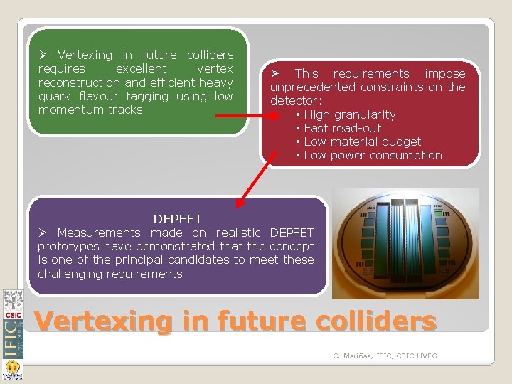
Ø Vertexing in future colliders requires excellent vertex reconstruction and efficient heavy quark flavour tagging using low momentum tracks Ø This requirements impose unprecedented constraints on the detector: • High granularity • Fast read-out • Low material budget • Low power consumption DEPFET Ø Measurements made on realistic DEPFET prototypes have demonstrated that the concept is one of the principal candidates to meet these challenging requirements Vertexing in future colliders C. Mariñas, IFIC, CSIC-UVEG

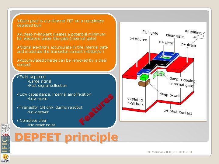
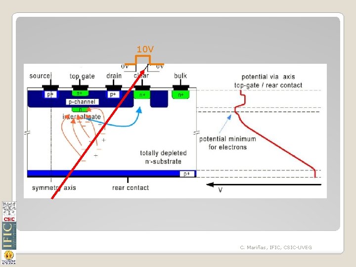
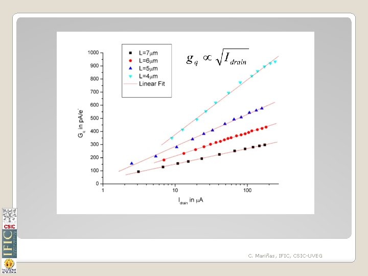
ØEach pixel is a p-channel FET on a completely depleted bulk ØA deep n-implant creates a potential minimum for electrons under the gate (internal gate) ØSignal electrons accumulate in the internal gate and modulate the transistor current (400 p. A/e -) ØAccumulated charge can be removed by a clear contact üFully depleted • Large signal • Fast signal collection üLow capacitance, internal amplification • Low noise üTransistor ON only during readout • Low power üComplete clear • No reset noise Fe u t a s e r DEPFET principle C. Mariñas, IFIC, CSIC-UVEG

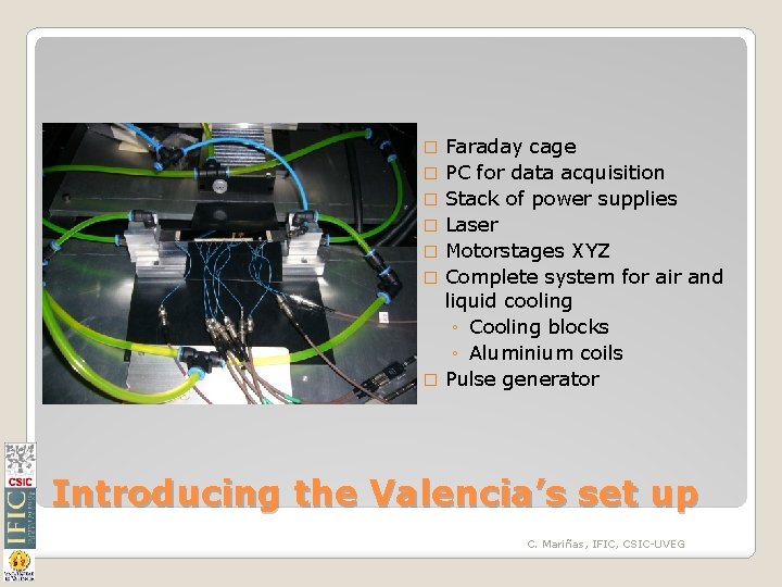
� � � � Faraday cage PC for data acquisition Stack of power supplies Laser Motorstages XYZ Complete system for air and liquid cooling ◦ Cooling blocks ◦ Aluminium coils Pulse generator Introducing the Valencia’s set up C. Mariñas, IFIC, CSIC-UVEG

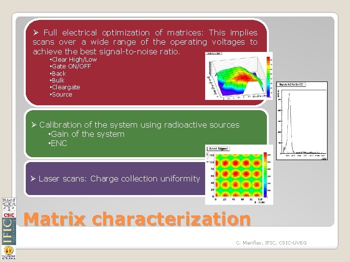
Ø Full electrical optimization of matrices: This implies scans over a wide range of the operating voltages to achieve the best signal-to-noise ratio. • Clear High/Low • Gate ON/OFF • Back • Bulk • Cleargate • Source Ø Calibration of the system using radioactive sources • Gain of the system • ENC Ø Laser scans: Charge collection uniformity Matrix characterization C. Mariñas, IFIC, CSIC-UVEG

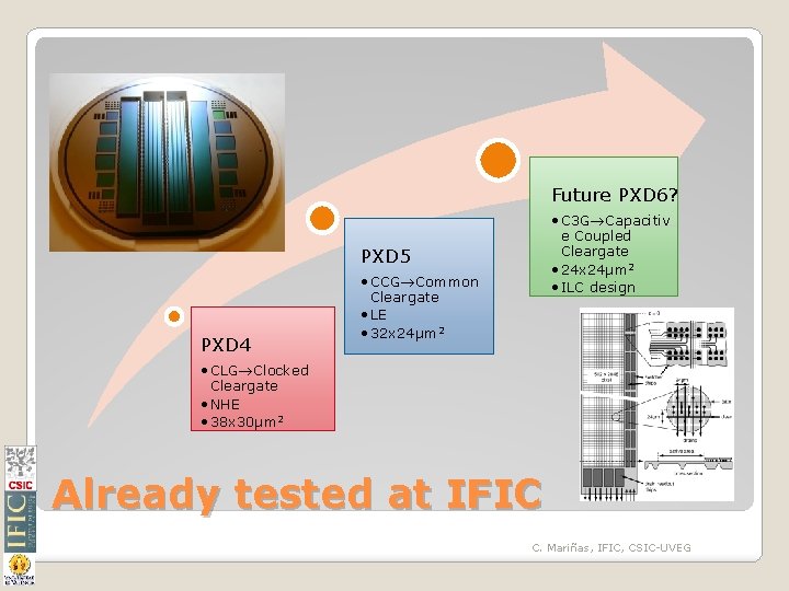
Future PXD 6? • C 3 G Capacitiv e Coupled Cleargate • 24 x 24μm 2 • ILC design PXD 5 PXD 4 • CCG Common Cleargate • LE • 32 x 24μm 2 • CLG Clocked Cleargate • NHE • 38 x 30μm 2 Already tested at IFIC C. Mariñas, IFIC, CSIC-UVEG

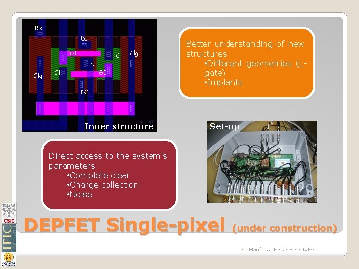
Blk D 1 G 1 Cl Clg S Clg Cl G 2 Better understanding of new structures • Different geometries (Lgate) • Implants D 2 Inner structure Set-up Direct access to the system’s parameters • Complete clear • Charge collection • Noise DEPFET Single-pixel (under construction) C. Mariñas, IFIC, CSIC-UVEG

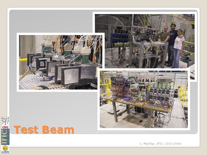
Test Beam C. Mariñas, IFIC, CSIC-UVEG

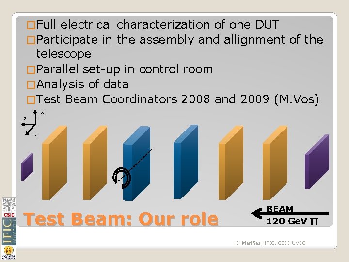
� Full electrical characterization of one DUT � Participate in the assembly and allignment of the telescope � Parallel set-up in control room � Analysis of data � Test Beam Coordinators 2008 and 2009 (M. Vos) x z y Test Beam: Our role BEAM 120 Ge. V ∏ C. Mariñas, IFIC, CSIC-UVEG

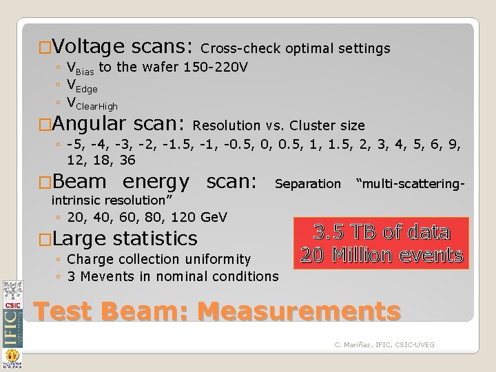
�Voltage scans: Cross-check optimal settings to the wafer 150 -220 V ◦ VBias ◦ VEdge ◦ VClear. High �Angular scan: Resolution vs. Cluster size ◦ -5, -4, -3, -2, -1. 5, -1, -0. 5, 0, 0. 5, 1, 1. 5, 2, 3, 4, 5, 6, 9, 12, 18, 36 �Beam energy scan: Separation “multi-scattering- intrinsic resolution” ◦ 20, 40, 60, 80, 120 Ge. V �Large statistics ◦ Charge collection uniformity ◦ 3 Mevents in nominal conditions 3. 5 TB of data 20 Million events Test Beam: Measurements C. Mariñas, IFIC, CSIC-UVEG

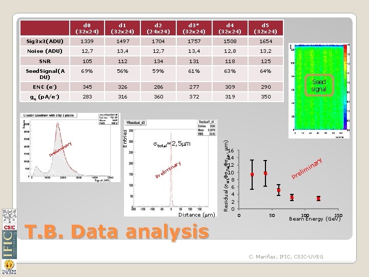
d 2 (24 x 24) d 3* (32 x 24) d 4 (32 x 24) d 5 (32 x 24) Sig 3 x 3(ADU) 1339 1497 1704 1757 1508 1654 Noise (ADU) 12, 7 13, 4 12, 8 13, 2 SNR 105 112 134 131 118 125 Seed. Signal(A DU) 69% 56% 59% 61% 63% 64% ENC (e-) 345 326 286 277 309 290 gq (p. A/e-) 283 316 360 372 319 350 ry ina lim stotal=2, 5 mm e Pr ry m eli Pr ina Distance (mm) T. B. Data analysis Residual (s. MSÅs. TelÅs. Int, mm) d 1 (32 x 24) Entries d 0 (32 x 24) 16 14 12 10 8 6 4 2 0 Seed signal ry m eli Pr 0 50 ina 100 150 Beam Energy (Ge. V) C. Mariñas, IFIC, CSIC-UVEG

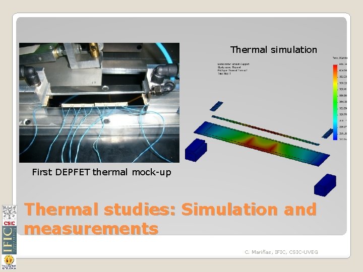
Thermal simulation First DEPFET thermal mock-up Thermal studies: Simulation and measurements C. Mariñas, IFIC, CSIC-UVEG

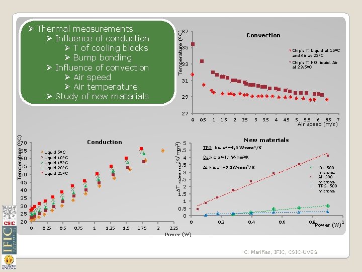
Ø Thermal measurements Ø Influence of conduction Ø T of cooling blocks Ø Bump bonding Ø Influence of convection Ø Air speed Ø Air temperature Ø Study of new materials Temperature (ºC) 37 Convection 35 Chip's T. Liquid at 15ºC and Air at 22ºC Chip's T. NO liquid. Air at 23. 5ºC 33 31 29 27 Temperature (ºC) 0 Conduction 65 Liquid Liquid 60 45 normalized 40 DT 55 5ºC 10ºC 15ºC 20ºC 25ºC 50 35 30 25 20 0 0. 25 0. 75 1 1. 25 1. 75 2 1 1. 5 2 2. 5 3 3. 5 4 4. 5 5 5. 5 6 6. 5 7 Air speed (m/s) New materials 5 4 3. 5 3 2. 5 2 1. 5 1 0. 5 0 (K/mm 2) 70 0. 5 TPG: k a a-1=4, 3 W·mm 2/K Cu: k a a-1=1, 1 W·mm 2/K Al: k a a-1=0, 2 W·mm 2/K 0 2. 25 Power (W) 0. 2 0. 4 Cu. 500 microns. Al. 300 microns. TPG. 500 microns. 0. 6 0. 8 1 Power (W) C. Mariñas, IFIC, CSIC-UVEG

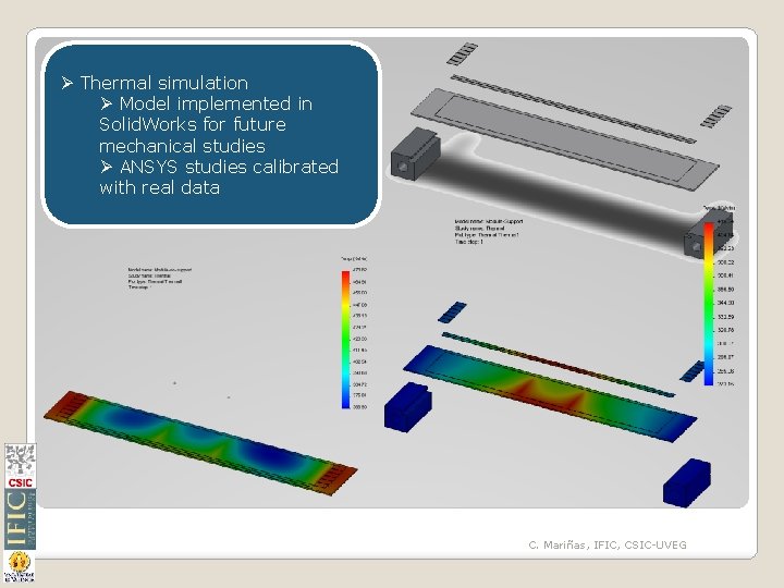
Ø Thermal simulation Ø Model implemented in Solid. Works for future mechanical studies Ø ANSYS studies calibrated with real data C. Mariñas, IFIC, CSIC-UVEG

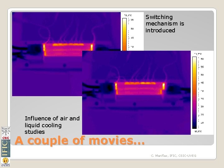
Switching mechanism is introduced Influence of air and liquid cooling studies A couple of movies… C. Mariñas, IFIC, CSIC-UVEG

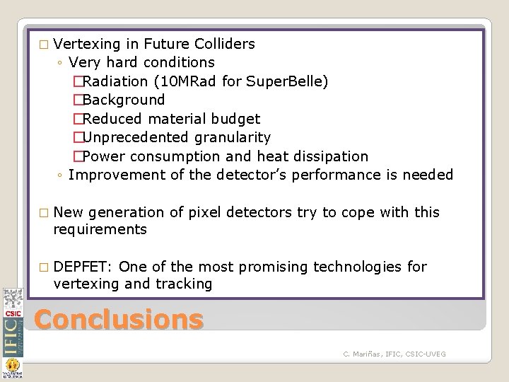
� Vertexing in Future Colliders ◦ Very hard conditions �Radiation (10 MRad for Super. Belle) �Background �Reduced material budget �Unprecedented granularity �Power consumption and heat dissipation ◦ Improvement of the detector’s performance is needed � New generation of pixel detectors try to cope with this requirements � DEPFET: One of the most promising technologies for vertexing and tracking Conclusions C. Mariñas, IFIC, CSIC-UVEG

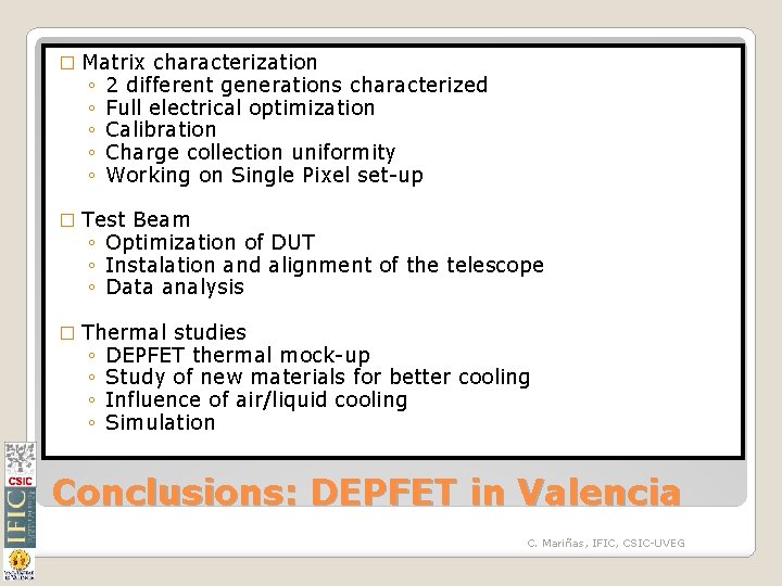
� Matrix characterization ◦ 2 different generations characterized ◦ Full electrical optimization ◦ Calibration ◦ Charge collection uniformity ◦ Working on Single Pixel set-up � Test Beam ◦ Optimization of DUT ◦ Instalation and alignment of the telescope ◦ Data analysis � Thermal studies ◦ DEPFET thermal mock-up ◦ Study of new materials for better cooling ◦ Influence of air/liquid cooling ◦ Simulation Conclusions: DEPFET in Valencia C. Mariñas, IFIC, CSIC-UVEG

Backup slides C. Mariñas, IFIC, CSIC-UVEG

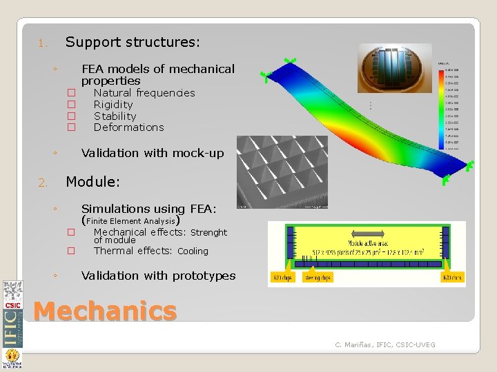
Support structures: 1. ◦ FEA models of mechanical properties � � ◦ Natural frequencies Rigidity Stability Deformations Validation with mock-up Module: 2. ◦ ◦ Simulations using FEA: (Finite Element Analysis) � Mechanical effects: Strenght � Thermal effects: Cooling of module Validation with prototypes Mechanics C. Mariñas, IFIC, CSIC-UVEG

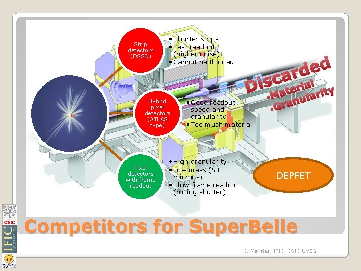
Strip detectors (DSSD) • Shorter strips • Fast readout (higher noise) • Cannot be thinned Hybrid pixel detectors (ATLAS type) Pixel detectors with frame readout d e d ar c rial s i D ate • Good readout speed and granularity • Too much material • High granularity • Low mass (50 microns) • Slow frame readout (rolling shutter) y • M nularit • Gra DEPFET Competitors for Super. Belle C. Mariñas, IFIC, CSIC-UVEG

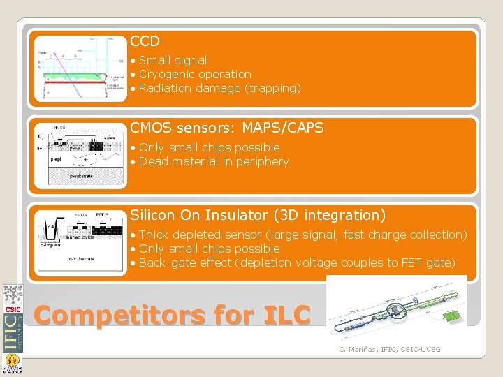
CCD • Small signal • Cryogenic operation • Radiation damage (trapping) CMOS sensors: MAPS/CAPS • Only small chips possible • Dead material in periphery Silicon On Insulator (3 D integration) • Thick depleted sensor (large signal, fast charge collection) • Only small chips possible • Back-gate effect (depletion voltage couples to FET gate) Competitors for ILC C. Mariñas, IFIC, CSIC-UVEG

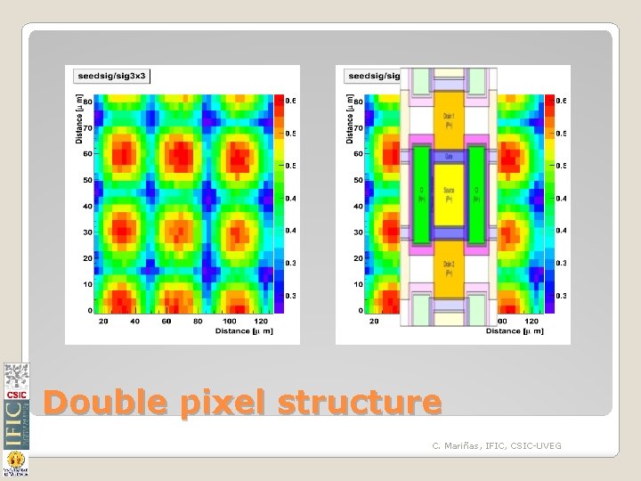
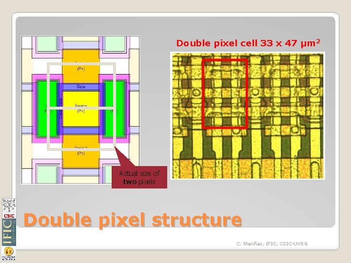
Double pixel structure C. Mariñas, IFIC, CSIC-UVEG

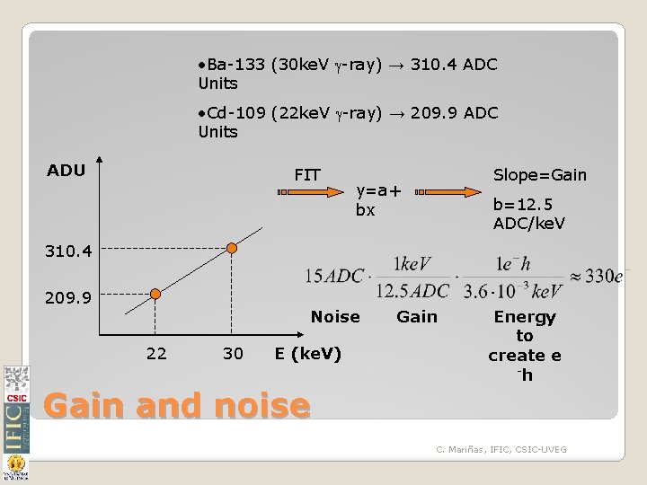
• Ba-133 (30 ke. V g-ray) → 310. 4 ADC Units • Cd-109 (22 ke. V g-ray) → 209. 9 ADC Units ADU FIT Slope=Gain y=a+ bx b=12. 5 ADC/ke. V 310. 4 209. 9 Noise 22 30 E (ke. V) Gain Energy to create e -h Gain and noise C. Mariñas, IFIC, CSIC-UVEG

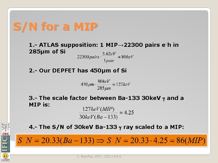
S/N for a MIP 1. - ATLAS supposition: 1 MIP→ 22300 pairs e-h in 285μm of Si 2. - Our DEPFET has 450μm of Si 3. - The scale factor between Ba-133 30 ke. V g and a MIP is: 4. - The S/N of 30 ke. V Ba-133 g ray scaled to a MIP: C. Mariñas, IFIC, CSIC-UVEG

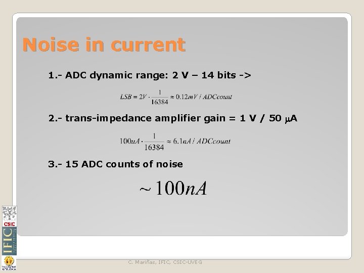
Noise in current 1. - ADC dynamic range: 2 V – 14 bits -> 2. - trans-impedance amplifier gain = 1 V / 50 m. A 3. - 15 ADC counts of noise C. Mariñas, IFIC, CSIC-UVEG

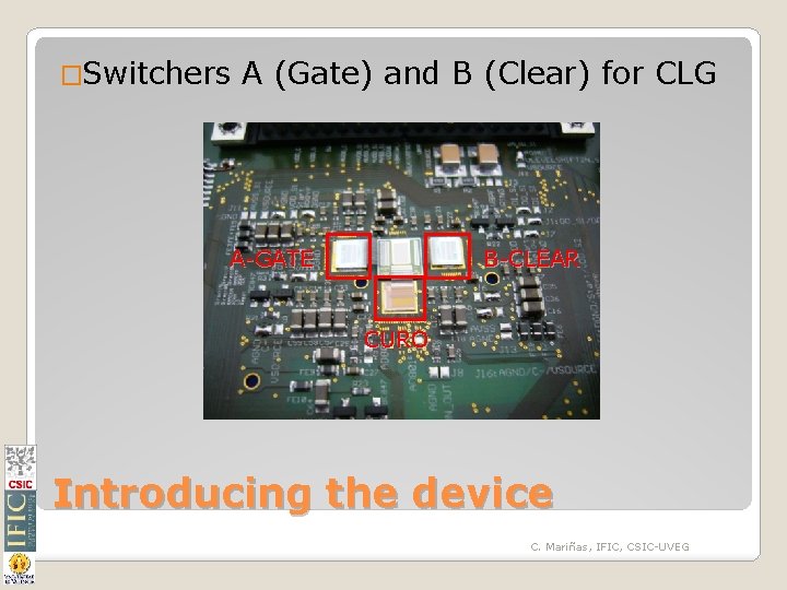
�Switchers A (Gate) and B (Clear) for CLG A-GATE B-CLEAR CURO Introducing the device C. Mariñas, IFIC, CSIC-UVEG

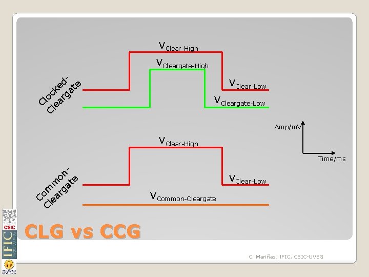
VClear-High VCleargate-High d e ate k oc arg l C le C VClear-Low VCleargate-Low Amp/m. V VClear-High Time/ms n o e m at m rg o C lea C VClear-Low VCommon-Cleargate CLG vs CCG C. Mariñas, IFIC, CSIC-UVEG

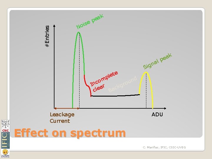
#Entries ise o N ak e p l a ign te e l p m nd o u c ro In ar g k c cle Ba Leackage Current S k a pe ADU Effect on spectrum C. Mariñas, IFIC, CSIC-UVEG

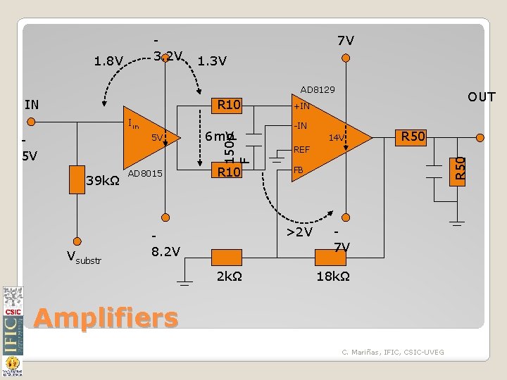
3. 2 V 1. 8 V 7 V 1. 3 V AD 8129 Iin 5 V 5 V 39 kΩ Vsubstr AD 8015 6 m. V R 10 -IN 14 V 2 kΩ R 50 REF FB >2 V 8. 2 V OUT +IN R 50 R 10 150 p F IN 7 V 18 kΩ Amplifiers C. Mariñas, IFIC, CSIC-UVEG

10 V C. Mariñas, IFIC, CSIC-UVEG

C. Mariñas, IFIC, CSIC-UVEG

Double pixel cell 33 x 47 µm 2 Actual size of two pixels Double pixel structure C. Mariñas, IFIC, CSIC-UVEG

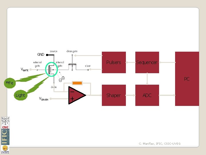
GND Pulsers Sequencer VGATE PC 55 Fe Light VDRAIN Shaper ADC C. Mariñas, IFIC, CSIC-UVEG

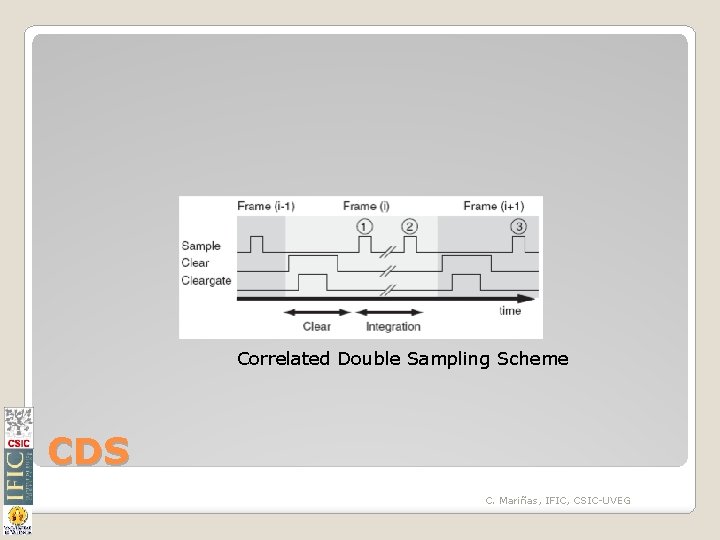
Correlated Double Sampling Scheme CDS C. Mariñas, IFIC, CSIC-UVEG