Operation of the Full Format DSSC Pixel Readout
- Slides: 16

Operation of the Full Format DSSC Pixel Readout ASIC for the European XFEL Jan Soldat, Heidelberg University for the DSSC ASIC design groups D. Comotti 4, F. Erdinger 1, C. Fiorini 3, P. Fischer 1, K. Hansen 2, P. Kalavakuru 2, M. Kirchgessner 1, M. Manghisoni 4, B. Nasri 3, M. Porro 5, C. Reckleben 2, J. Szymanski 2 (Heidelberg Univ. 1, DESY 2, Politecnico di Milano 3, Univ. de Bergamo 4, MPE Munich 5) 1 13 th Pisa Meeting

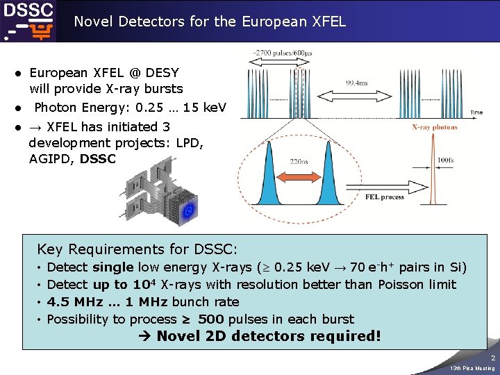
Novel Detectors for the European XFEL ● European XFEL @ DESY will provide X-ray bursts ● Photon Energy: 0. 25 … 15 ke. V ● → XFEL has initiated 3 development projects: LPD, AGIPD, DSSC Key Requirements for DSSC: • • Detect single low energy X-rays ( 0. 25 ke. V → 70 e-h+ pairs in Si) Detect up to 104 X-rays with resolution better than Poisson limit 4. 5 MHz … 1 MHz bunch rate Possibility to process 500 pulses in each burst Novel 2 D detectors required! 2 13 th Pisa Meeting

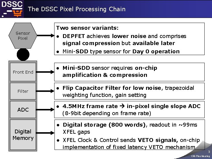
The DSSC Pixel Processing Chain Sensor Pixel Two sensor variants: ● DEPFET achieves lower noise and comprises signal compression but available later ● Mini-SDD type sensor for Day 0 operation Front End Filter ASIC Pixel ADC Digital Memory ● Mini-SDD sensor requires on-chip amplification & compression ● Flip Capacitor Filter for low noise, trapezoidal weighting function, gain setting ● 4. 5 MHz frame rate in-pixel single slope ADC (8 -9 bit depending on frame rate) ● Digital storage (800 words), readout in ~99 ms XFEL gaps ● XFEL Clock & Control sends VETO signals, on-chip implementation of fixed latency VETO mechanism 3 13 th Pisa Meeting

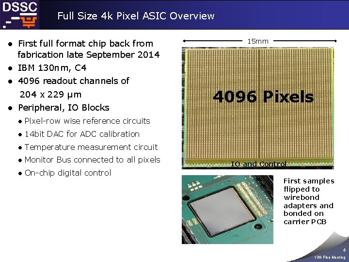
Full Size 4 k Pixel ASIC Overview ● First full format chip back from fabrication late September 2014 ● IBM 130 nm, C 4 ● 4096 readout channels of 204 x 229 µm ● Peripheral, IO Blocks 15 mm 4096 Pixels ● Pixel-row wise reference circuits ● 14 bit DAC for ADC calibration ● Temperature measurement circuit ● Monitor Bus connected to all pixels ● On-chip digital control IO and Control First samples flipped to wirebond adapters and bonded on carrier PCB 4 13 th Pisa Meeting

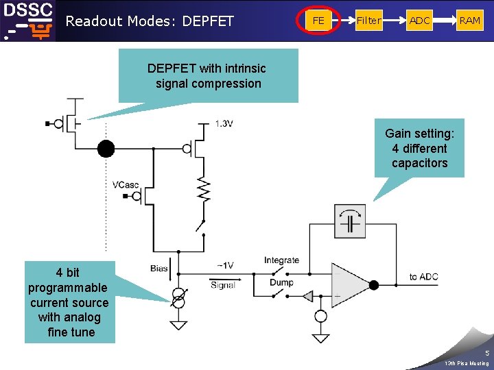
Readout Modes: DEPFET FE Filter RAM ADC DEPFET with intrinsic signal compression Gain setting: 4 different capacitors 4 bit programmable current source with analog fine tune 5 13 th Pisa Meeting

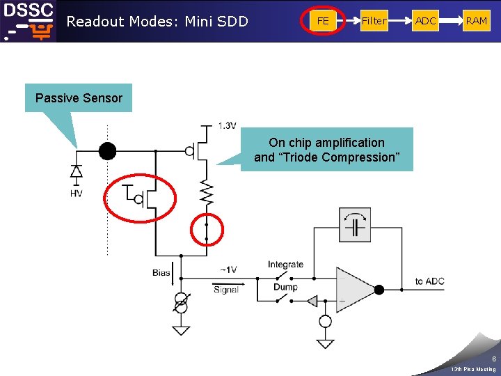
Readout Modes: Mini SDD FE Filter ADC RAM Passive Sensor On chip amplification and “Triode Compression” 6 13 th Pisa Meeting

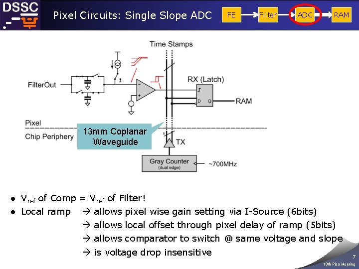
Pixel Circuits: Single Slope ADC FE Filter ADC RAM 13 mm Coplanar Waveguide ● Vref of Comp = Vref of Filter! ● Local ramp allows pixel wise gain setting via I-Source (6 bits) allows local offset through pixel delay of ramp (5 bits) allows comparator to switch @ same voltage and slope is voltage drop insensitive 7 13 th Pisa Meeting

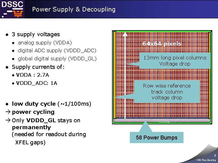
Power Supply & Decoupling ● 3 supply voltages ● analog supply (VDDA) 64 x 64 pixels ● digital ADC supply (VDDD_ADC) ● global digital supply (VDDD_GL) ● Supply currents of: 13 mm long pixel columns Voltage drop ● VDDA : 2. 7 A ● VDDD_ADC: 1 A ● low duty cycle (~1/100 ms) power cycling Only VDDD_GL stays on permanently (needed for readout during XFEL gaps) Row wise reference track column voltage drop 58 Power Bumps 8 13 th Pisa Meeting

Chip operation results 9 13 th Pisa Meeting

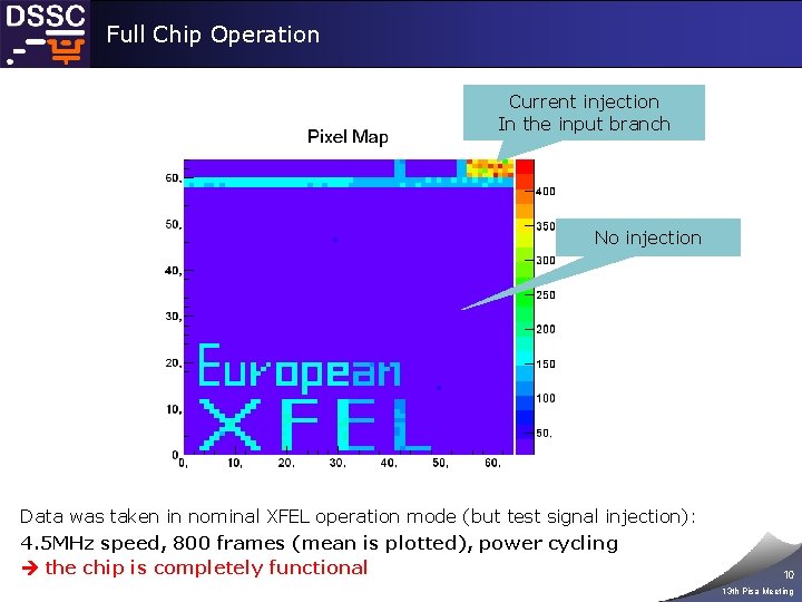
Full Chip Operation Current injection In the input branch No injection Data was taken in nominal XFEL operation mode (but test signal injection): 4. 5 MHz speed, 800 frames (mean is plotted), power cycling the chip is completely functional 10 13 th Pisa Meeting

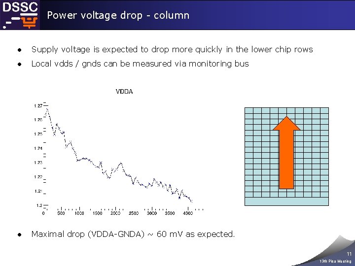
Power voltage drop - column ● Supply voltage is expected to drop more quickly in the lower chip rows ● Local vdds / gnds can be measured via monitoring bus ● Maximal drop (VDDA-GNDA) ~ 60 m. V as expected. 11 13 th Pisa Meeting

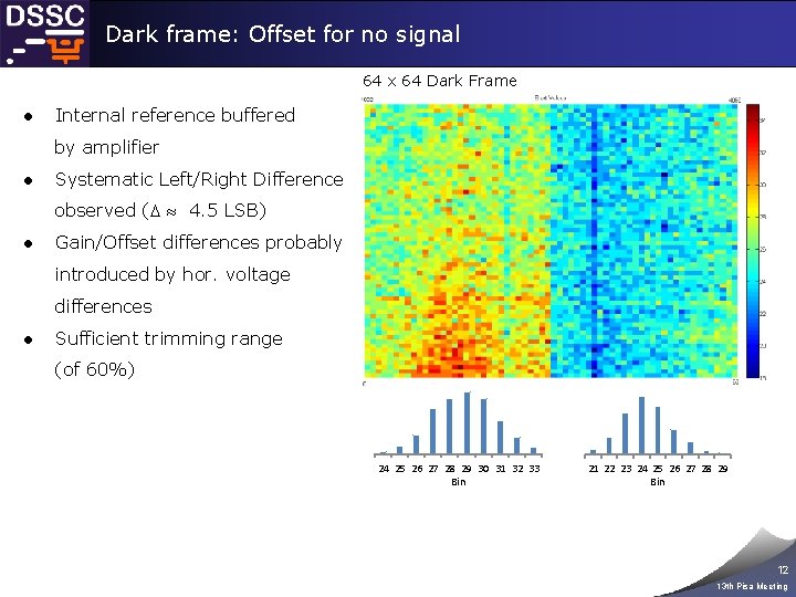
Dark frame: Offset for no signal 64 x 64 Dark Frame ● Internal reference buffered by amplifier ● Systematic Left/Right Difference observed ( 4. 5 LSB) ● Gain/Offset differences probably introduced by hor. voltage differences ● Sufficient trimming range (of 60%) 24 25 26 27 28 29 30 31 32 33 Bin 21 22 23 24 25 26 27 28 29 Bin 12 13 th Pisa Meeting

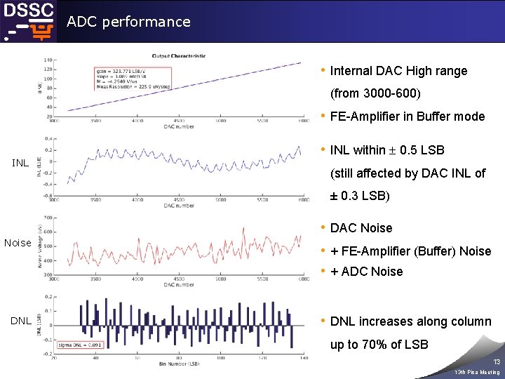
ADC performance • Internal DAC High range (from 3000 -600) • FE-Amplifier in Buffer mode INL • INL within 0. 5 LSB (still affected by DAC INL of ± 0. 3 LSB) Noise DNL • DAC Noise • + FE-Amplifier (Buffer) Noise • + ADC Noise • DNL increases along column up to 70% of LSB 13 13 th Pisa Meeting

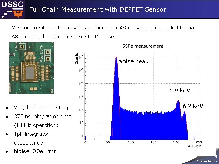
Full Chain Measurement with DEPFET Sensor Measurement was taken with a mini matrix ASIC (same pixel as full format ASIC) bump bonded to an 8 x 8 DEPFET sensor Noise peak 5. 9 ke. V ● Very high gain setting ● 370 ns integration time 6. 2 ke. V (1 MHz operation) ● 1 p. F integrator capacitance ● Noise: 20 e- rms 14 13 th Pisa Meeting

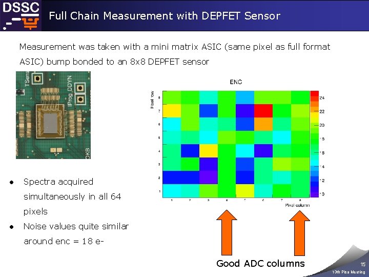
Full Chain Measurement with DEPFET Sensor Measurement was taken with a mini matrix ASIC (same pixel as full format ASIC) bump bonded to an 8 x 8 DEPFET sensor ● Spectra acquired simultaneously in all 64 pixels ● Noise values quite similar around enc = 18 e- Good ADC columns 15 13 th Pisa Meeting

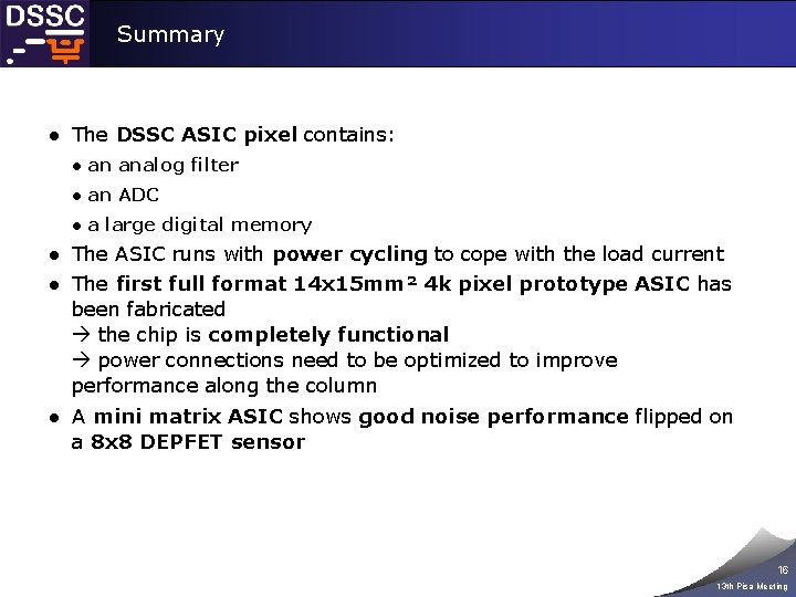
Summary ● The DSSC ASIC pixel contains: ● an analog filter ● an ADC ● a large digital memory ● The ASIC runs with power cycling to cope with the load current ● The first full format 14 x 15 mm² 4 k pixel prototype ASIC has been fabricated the chip is completely functional power connections need to be optimized to improve performance along the column ● A mini matrix ASIC shows good noise performance flipped on a 8 x 8 DEPFET sensor 16 13 th Pisa Meeting