CPEEE 421 Microcomputers The MSP 430 System Architecture
![Interrupt Service Routines n Interrupt Service Routine declaration // Func. declaration Interrupt[int_vector] void my. Interrupt Service Routines n Interrupt Service Routine declaration // Func. declaration Interrupt[int_vector] void my.](https://slidetodoc.com/presentation_image/25b7e96897c3c89f14371366745f5905/image-15.jpg)

![Battery Life n n Battery Capacity BC – [m. Ah] Battery Life n n Battery Life n n Battery Capacity BC – [m. Ah] Battery Life n n](https://slidetodoc.com/presentation_image/25b7e96897c3c89f14371366745f5905/image-61.jpg)
- Slides: 116

CPE/EE 421 Microcomputers: The MSP 430 System Architecture Instructor: Dr Aleksandar Milenkovic Lecture Notes CPE/EE 421/521 Microcomputers

Outline n n n MSP 430: System Architecture System Resets, Interrupts, and Operating Modes Basic Clock Module Watchdog Timer CPE/EE 421/521 Microcomputers 2

MSP 430: System Resets, Interrupts, and Operating Modes CPE/EE 421/521 Microcomputers

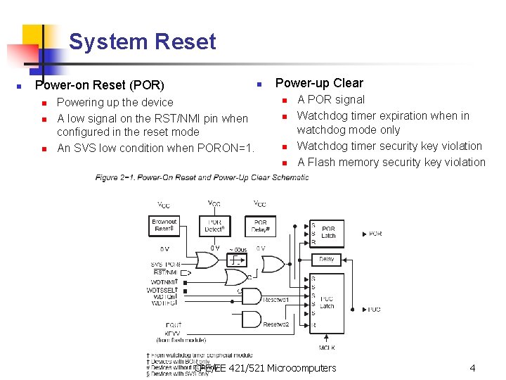
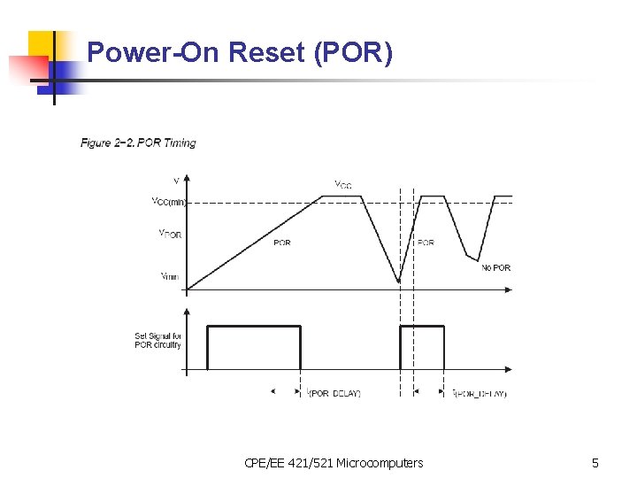
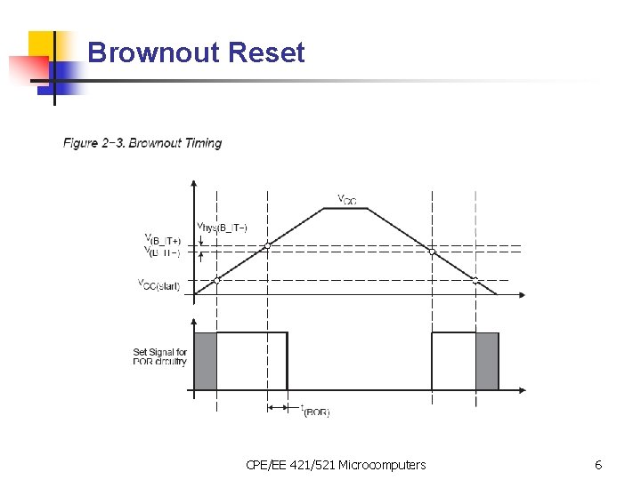
System Reset n Power-on Reset (POR) n n Powering up the device A low signal on the RST/NMI pin when configured in the reset mode An SVS low condition when PORON=1. Power-up Clear n n A POR signal Watchdog timer expiration when in watchdog mode only Watchdog timer security key violation A Flash memory security key violation CPE/EE 421/521 Microcomputers 4

Power-On Reset (POR) CPE/EE 421/521 Microcomputers 5

Brownout Reset CPE/EE 421/521 Microcomputers 6

Software initialization n n Your SW must initialize the MSP 430 Initialize the SP, typically to the top of RAM. Initialize the watchdog to the requirements of the application. Configure peripheral modules to the requirements of the application. Additionally, the watchdog timer, oscillator fault, and flash memory flags can be evaluated to determine the source of the reset. CPE/EE 421/521 Microcomputers 7

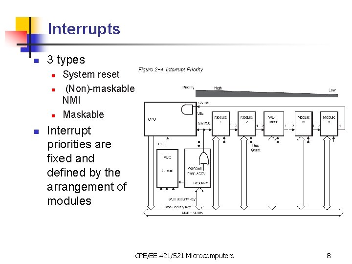
Interrupts n 3 types n n System reset (Non)-maskable NMI Maskable Interrupt priorities are fixed and defined by the arrangement of modules CPE/EE 421/521 Microcomputers 8

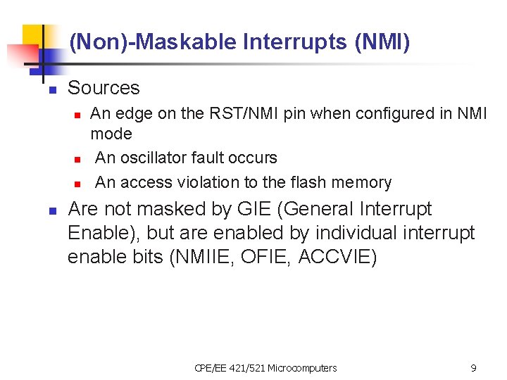
(Non)-Maskable Interrupts (NMI) n Sources n n An edge on the RST/NMI pin when configured in NMI mode An oscillator fault occurs An access violation to the flash memory Are not masked by GIE (General Interrupt Enable), but are enabled by individual interrupt enable bits (NMIIE, OFIE, ACCVIE) CPE/EE 421/521 Microcomputers 9

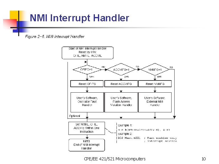
NMI Interrupt Handler CPE/EE 421/521 Microcomputers 10

Maskable Interrupts n n n Caused by peripherals with interrupt capability Each can be disabled individually by an interrupt enable bit All can be disabled by GIE bit in the status register CPE/EE 421/521 Microcomputers 11

Interrupt acceptance n n n n 1) Any currently executing instruction is completed. 2) The PC, which points to the next instruction, is pushed onto the stack. 3) The SR is pushed onto the stack. 4) The interrupt with the highest priority is selected if multiple interrupts occurred during the last instruction and are pending for service. 5) The interrupt request flag resets automatically on single-source flags. Multiple source flags remain set for servicing by software. 6) The SR is cleared with the exception of SCG 0, which is left unchanged. This terminates any low-power mode. Because the GIE bit is cleared, further interrupts are disabled. 7) The content of the interrupt vector is loaded into the PC: the program continues with the interrupt service routine at that address. Takes 6 cc to execute CPE/EE 421/521 Microcomputers 12

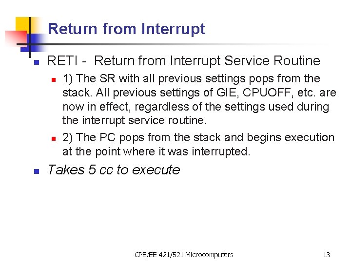
Return from Interrupt n RETI - Return from Interrupt Service Routine n n n 1) The SR with all previous settings pops from the stack. All previous settings of GIE, CPUOFF, etc. are now in effect, regardless of the settings used during the interrupt service routine. 2) The PC pops from the stack and begins execution at the point where it was interrupted. Takes 5 cc to execute CPE/EE 421/521 Microcomputers 13

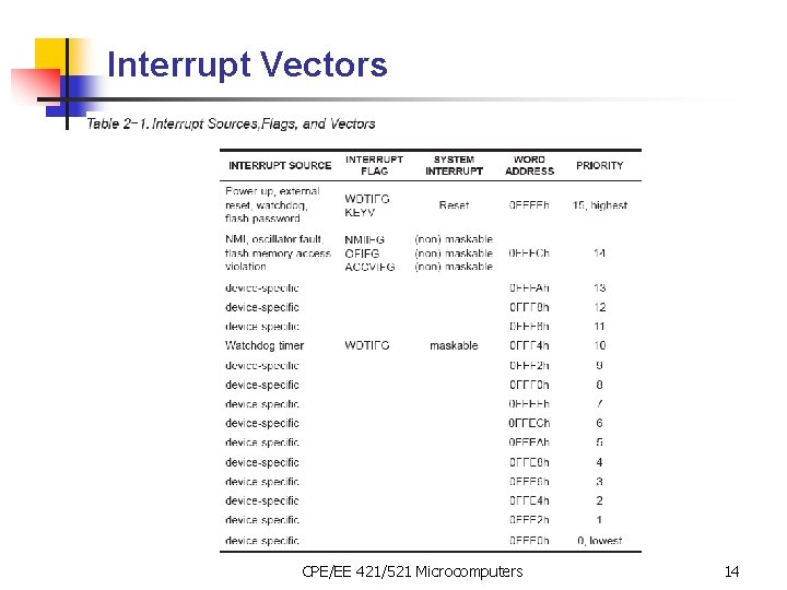
Interrupt Vectors CPE/EE 421/521 Microcomputers 14
![Interrupt Service Routines n Interrupt Service Routine declaration Func declaration Interruptintvector void my Interrupt Service Routines n Interrupt Service Routine declaration // Func. declaration Interrupt[int_vector] void my.](https://slidetodoc.com/presentation_image/25b7e96897c3c89f14371366745f5905/image-15.jpg)
Interrupt Service Routines n Interrupt Service Routine declaration // Func. declaration Interrupt[int_vector] void my. ISR (Void); Interrupt[int_vector] void my. ISR (Void) { // ISR code } q EXAMPLE Interrupt[TIMERA 0_VECTOR] void my. ISR (Void); Interrupt[TIMERA 0_VECTOR] void my. ISR (Void) { // ISR code } CPE/EE 421/521 Microcomputers 15

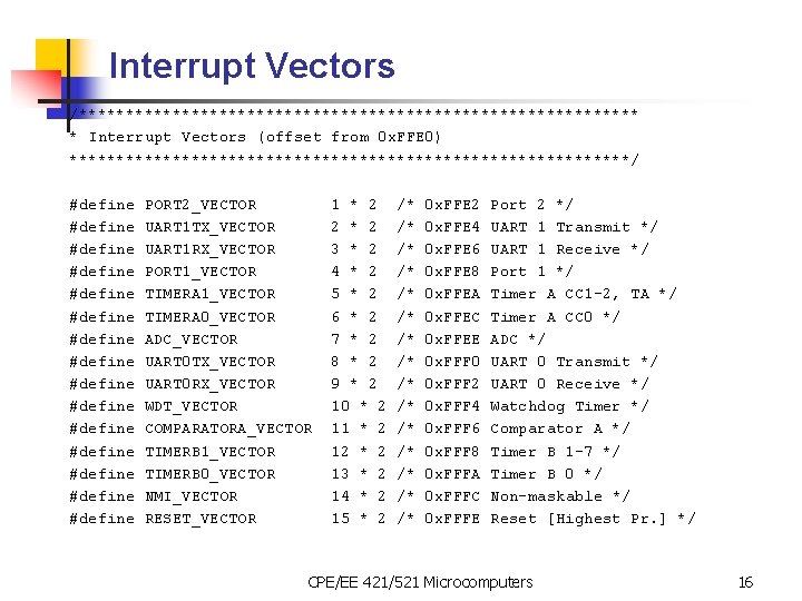
Interrupt Vectors /****************************** * Interrupt Vectors (offset from 0 x. FFE 0) ******************************/ #define #define #define #define PORT 2_VECTOR UART 1 TX_VECTOR UART 1 RX_VECTOR PORT 1_VECTOR TIMERA 0_VECTOR ADC_VECTOR UART 0 TX_VECTOR UART 0 RX_VECTOR WDT_VECTOR COMPARATORA_VECTOR TIMERB 1_VECTOR TIMERB 0_VECTOR NMI_VECTOR RESET_VECTOR 1 * 2 2 * 2 3 * 2 4 * 2 5 * 2 6 * 2 7 * 2 8 * 2 9 * 2 10 * 2 11 * 2 12 * 2 13 * 2 14 * 2 15 * 2 /* /* /* /* 0 x. FFE 2 0 x. FFE 4 0 x. FFE 6 0 x. FFE 8 0 x. FFEA 0 x. FFEC 0 x. FFEE 0 x. FFF 0 0 x. FFF 2 0 x. FFF 4 0 x. FFF 6 0 x. FFF 8 0 x. FFFA 0 x. FFFC 0 x. FFFE Port 2 */ UART 1 Transmit */ UART 1 Receive */ Port 1 */ Timer A CC 1 -2, TA */ Timer A CC 0 */ ADC */ UART 0 Transmit */ UART 0 Receive */ Watchdog Timer */ Comparator A */ Timer B 1 -7 */ Timer B 0 */ Non-maskable */ Reset [Highest Pr. ] */ CPE/EE 421/521 Microcomputers 16

Operating Modes (to be discussed later) CPE/EE 421/521 Microcomputers 17

MSP 430: Basic Clock System CPE/EE 421/521 Microcomputers

Basic Clock System MSP 430 Clock System n n Low System Cost n Low Power Variety of operating modes driven by application, software selectable Support for the Burst Mode – when activated system starts and reacts rapidly Stability over voltage and temperature CPE/EE 421/521 Microcomputers 19

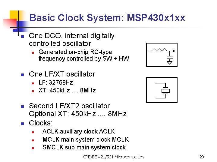
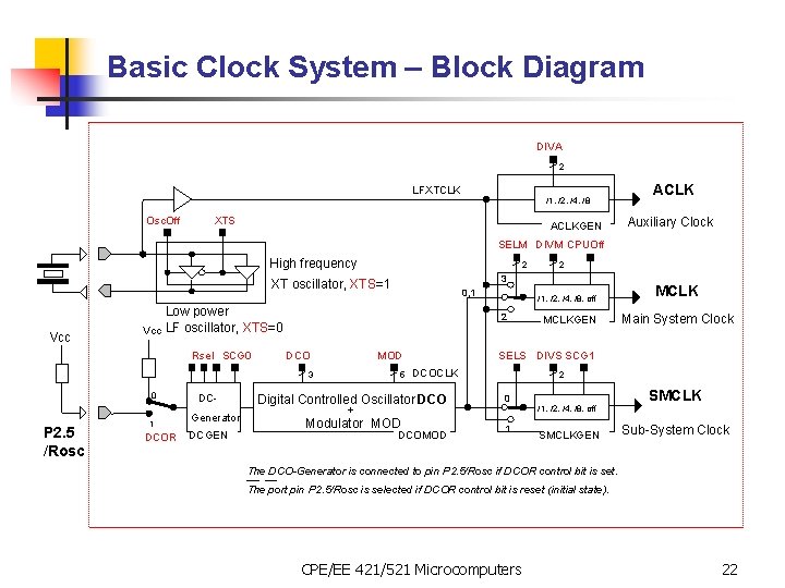
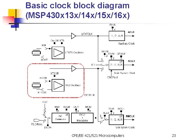
Basic Clock System: MSP 430 x 1 xx n One DCO, internal digitally controlled oscillator n n One LF/XT oscillator n n Generated on-chip RC-type frequency controlled by SW + HW LF: 32768 Hz XT: 450 k. Hz. . 8 MHz Second LF/XT 2 oscillator Optional XT: 450 k. Hz. . 8 MHz Clocks: n n n ACLK auxiliary clock ACLK MCLK main system clock MCLK SMCLK sub main system clock CPE/EE 421/521 Microcomputers 20

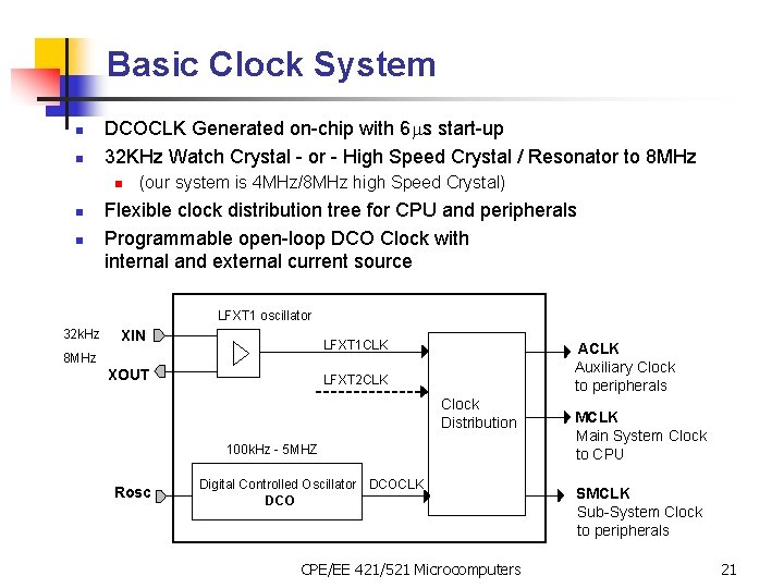
Basic Clock System n n DCOCLK Generated on-chip with 6 s start-up 32 KHz Watch Crystal - or - High Speed Crystal / Resonator to 8 MHz n n n (our system is 4 MHz/8 MHz high Speed Crystal) Flexible clock distribution tree for CPU and peripherals Programmable open-loop DCO Clock with internal and external current source LFXT 1 oscillator 32 k. Hz XIN LFXT 1 CLK 8 MHz XOUT ACLK Auxiliary Clock to peripherals LFXT 2 CLK Clock Distribution 100 k. Hz - 5 MHZ Rosc Digital Controlled Oscillator DCOCLK DCO CPE/EE 421/521 Microcomputers MCLK Main System Clock to CPU SMCLK Sub-System Clock to peripherals 21

Basic Clock System – Block Diagram DIVA 2 LFXTCLK Osc. Off /1, /2, /4, /8 XTS ACLKGEN ACLK Auxiliary Clock SELM DIVM CPUOff High frequency 2 XT oscillator, XTS=1 Vcc 2 DCO MOD 3 0 P 2. 5 /Rosc 0, 1 Low power Vcc LF oscillator, XTS=0 Rsel SCG 0 1 DCOR DCGenerator DCGEN 2 3 5 /1, /2, /4, /8, off MCLKGEN Main System Clock SELS DIVS SCG 1 DCOCLK 2 Digital Controlled Oscillator DCO 0 Modulator MOD 1 + DCOMOD /1, /2, /4, /8, off SMCLKGEN SMCLK Sub-System Clock The DCO-Generator is connected to pin P 2. 5/Rosc if DCOR control bit is set. The port pin P 2. 5/Rosc is selected if DCOR control bit is reset (initial state). CPE/EE 421/521 Microcomputers 22

Basic clock block diagram (MSP 430 x 13 x/14 x/15 x/16 x) CPE/EE 421/521 Microcomputers 23

Basic operation n n After POC (Power Up Clear) MCLK and SCLK are sourced by DCOCLK (approx. 800 KHz) and ACLK is sourced by LFXT 1 in LF mode Status register control bits SCG 0, SCG 1, OSCOFF, and CPUOFF configure the MSP 430 operating modes and enable or disable portions of the basic clock module n n n SCG 1 - when set, turns off the SMCLK SCG 0 - when set, turns off the DCO dc generator (if DCOCLK is not used for MCLK or SMCLK) OSCOFF - when set, turns off the LFXT 1 crystal oscillator (if LFXT 1 CLK is not use for MCLK or SMCLK) CPUOFF - when set, turns off the CPU DCOCTL, BCSCTL 1, and BCSCTL 2 registers configure the basic clock module The basic clock can be configured or reconfigured by software at any time during program execution CPE/EE 421/521 Microcomputers 24

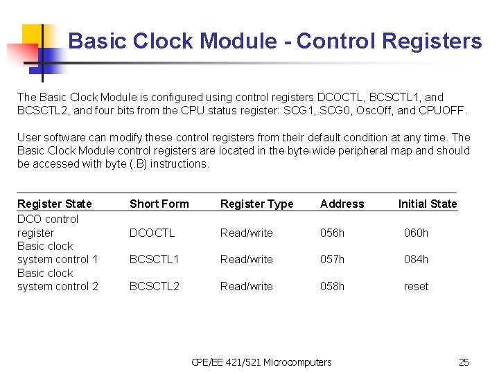
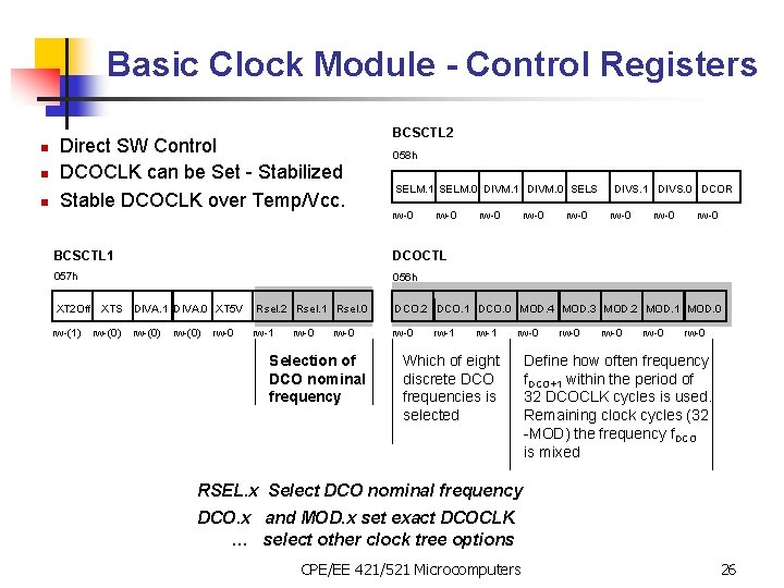
Basic Clock Module - Control Registers The Basic Clock Module is configured using control registers DCOCTL, BCSCTL 1, and BCSCTL 2, and four bits from the CPU status register: SCG 1, SCG 0, Osc. Off, and CPUOFF. User software can modify these control registers from their default condition at any time. The Basic Clock Module control registers are located in the byte-wide peripheral map and should be accessed with byte (. B) instructions. Register State DCO control register Basic clock system control 1 Basic clock system control 2 Short Form Register Type Address DCOCTL Read/write 056 h 060 h BCSCTL 1 Read/write 057 h 084 h BCSCTL 2 Read/write 058 h reset CPE/EE 421/521 Microcomputers Initial State 25

Basic Clock Module - Control Registers n n n Direct SW Control DCOCLK can be Set - Stabilized Stable DCOCLK over Temp/Vcc. BCSCTL 2 058 h SELM. 1 SELM. 0 DIVM. 1 DIVM. 0 SELS rw-0 BCSCTL 1 DCOCTL 057 h 056 h XT 2 Off XTS DIVA. 1 DIVA. 0 XT 5 V rw-(1) rw-(0) rw-0 Rsel. 2 Rsel. 1 Rsel. 0 rw-1 rw-0 Selection of DCO nominal frequency rw-0 DIVS. 1 DIVS. 0 DCOR rw-0 DCO. 2 DCO. 1 DCO. 0 MOD. 4 MOD. 3 MOD. 2 MOD. 1 MOD. 0 rw-1 rw-0 Which of eight discrete DCO frequencies is selected rw-0 Define how often frequency f. DCO+1 within the period of 32 DCOCLK cycles is used. Remaining clock cycles (32 -MOD) the frequency f. DCO is mixed RSEL. x Select DCO nominal frequency DCO. x and MOD. x set exact DCOCLK … select other clock tree options CPE/EE 421/521 Microcomputers 26

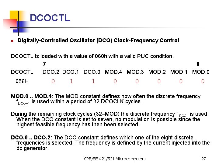
DCOCTL n Digitally-Controlled Oscillator (DCO) Clock-Frequency Control DCOCTL is loaded with a value of 060 h with a valid PUC condition. 7 0 DCOCTL DCO. 2 DCO. 1 DCO. 0 MOD. 4 MOD. 3 MOD. 2 MOD. 1 MOD. 0 056 H 0 1 1 0 0 0 MOD. 0. . MOD. 4: The MOD constant defines how often the discrete frequency f. DCO+1 is used within a period of 32 DCOCLK cycles. During the remaining clock cycles (32–MOD) the discrete frequency f DCO is used. When the DCO constant is set to seven, no modulation is possible since the highest feasible frequency has then been selected. DCO. 0. . DCO. 2: The DCO constant defines which one of the eight discrete frequencies is selected. The frequency is defined by the current injected into the dc generator. CPE/EE 421/521 Microcomputers 27

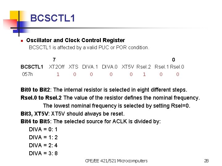
BCSCTL 1 n Oscillator and Clock Control Register BCSCTL 1 is affected by a valid PUC or POR condition. BCSCTL 1 057 h 7 0 XT 2 Off XTS DIVA. 1 DIVA. 0 XT 5 V Rsel. 2 Rsel. 1 Rsel. 0 1 0 0 Bit 0 to Bit 2: The internal resistor is selected in eight different steps. Rsel. 0 to Rsel. 2 The value of the resistor defines the nominal frequency. The lowest nominal frequency is selected by setting Rsel=0. Bit 3, XT 5 V: XT 5 V should always be reset. Bit 4 to Bit 5: The selected source for ACLK is divided by: DIVA = 0: 1 DIVA = 1: 2 DIVA = 2: 4 DIVA = 3: 8 CPE/EE 421/521 Microcomputers 28

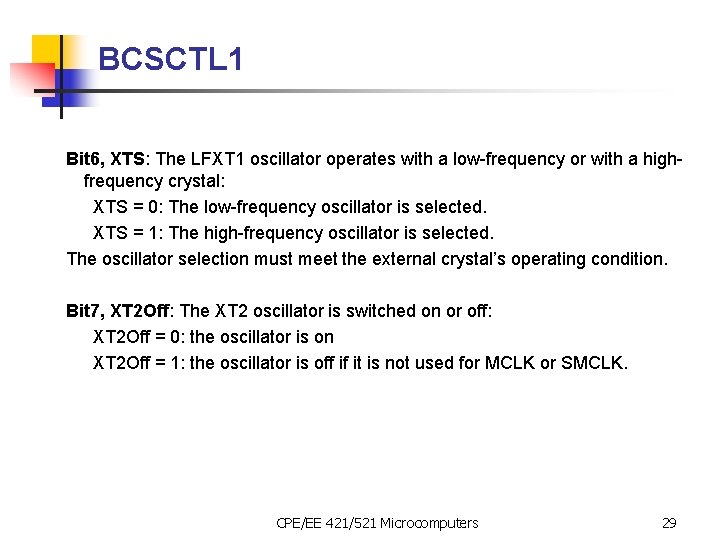
BCSCTL 1 Bit 6, XTS: The LFXT 1 oscillator operates with a low-frequency or with a highfrequency crystal: XTS = 0: The low-frequency oscillator is selected. XTS = 1: The high-frequency oscillator is selected. The oscillator selection must meet the external crystal’s operating condition. Bit 7, XT 2 Off: The XT 2 oscillator is switched on or off: XT 2 Off = 0: the oscillator is on XT 2 Off = 1: the oscillator is off if it is not used for MCLK or SMCLK. CPE/EE 421/521 Microcomputers 29

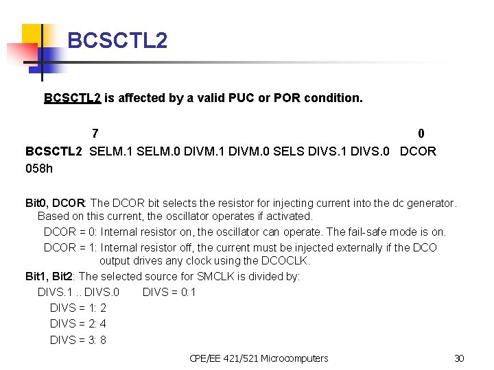
BCSCTL 2 is affected by a valid PUC or POR condition. 7 0 BCSCTL 2 SELM. 1 SELM. 0 DIVM. 1 DIVM. 0 SELS DIVS. 1 DIVS. 0 DCOR 058 h Bit 0, DCOR: The DCOR bit selects the resistor for injecting current into the dc generator. Based on this current, the oscillator operates if activated. DCOR = 0: Internal resistor on, the oscillator can operate. The fail-safe mode is on. DCOR = 1: Internal resistor off, the current must be injected externally if the DCO output drives any clock using the DCOCLK. Bit 1, Bit 2: The selected source for SMCLK is divided by: DIVS. 1. . DIVS. 0 DIVS = 0: 1 DIVS = 1: 2 DIVS = 2: 4 DIVS = 3: 8 CPE/EE 421/521 Microcomputers 30

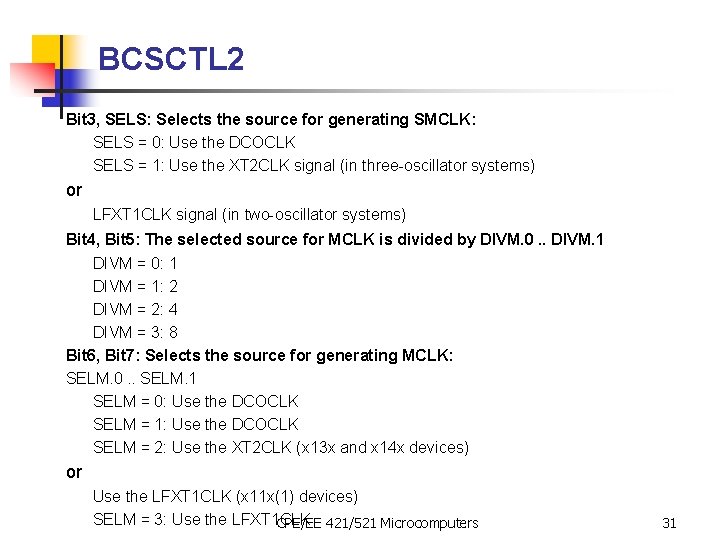
BCSCTL 2 Bit 3, SELS: Selects the source for generating SMCLK: SELS = 0: Use the DCOCLK SELS = 1: Use the XT 2 CLK signal (in three-oscillator systems) or LFXT 1 CLK signal (in two-oscillator systems) Bit 4, Bit 5: The selected source for MCLK is divided by DIVM. 0. . DIVM. 1 DIVM = 0: 1 DIVM = 1: 2 DIVM = 2: 4 DIVM = 3: 8 Bit 6, Bit 7: Selects the source for generating MCLK: SELM. 0. . SELM. 1 SELM = 0: Use the DCOCLK SELM = 1: Use the DCOCLK SELM = 2: Use the XT 2 CLK (x 13 x and x 14 x devices) or Use the LFXT 1 CLK (x 11 x(1) devices) SELM = 3: Use the LFXT 1 CLK CPE/EE 421/521 Microcomputers 31

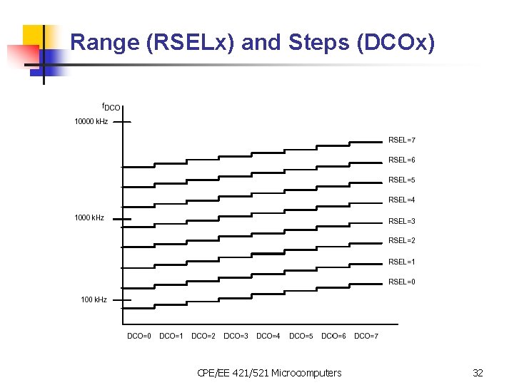
Range (RSELx) and Steps (DCOx) CPE/EE 421/521 Microcomputers 32

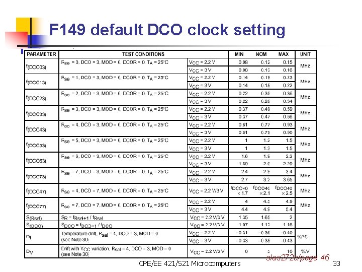
F 149 default DCO clock setting CPE/EE 421/521 Microcomputers slas 272 c/page 46 33

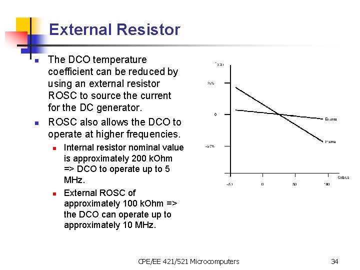
External Resistor n n The DCO temperature coefficient can be reduced by using an external resistor ROSC to source the current for the DC generator. ROSC also allows the DCO to operate at higher frequencies. n n Internal resistor nominal value is approximately 200 k. Ohm => DCO to operate up to 5 MHz. External ROSC of approximately 100 k. Ohm => the DCO can operate up to approximately 10 MHz. CPE/EE 421/521 Microcomputers 34

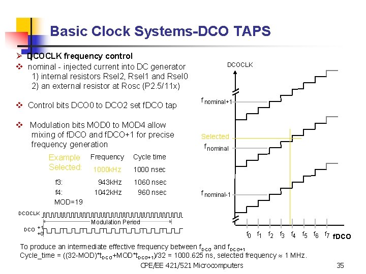
Basic Clock Systems-DCO TAPS Ø DCOCLK frequency control v nominal - injected current into DC generator 1) internal resistors Rsel 2, Rsel 1 and Rsel 0 2) an external resistor at Rosc (P 2. 5/11 x) v Control bits DCO 0 to DCO 2 set f. DCO tap v Modulation bits MOD 0 to MOD 4 allow mixing of f. DCO and f. DCO+1 for precise frequency generation Example Selected: f 3: f 4: MOD=19 Frequency Cycle time 1000 k. Hz 1000 nsec 943 k. Hz 1042 k. Hz 1060 nsec 960 nsec DCOCLK f nominal+1 Selected f nominal-1 DCOCLK DCO +1 +0 Modulation Period f 0 f 1 f 2 f 3 f 4 f 5 To produce an intermediate effective frequency between f. DCO and f. DCO+1 Cycle_time = ((32 -MOD)*t. DCO+MOD*t. DCO+1)/32 = 1000. 625 ns, selected frequency 1 MHz. CPE/EE 421/521 Microcomputers f 6 f 7 f. DCO 35

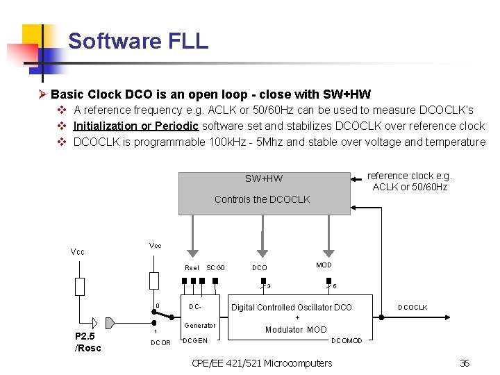
Software FLL Ø Basic Clock DCO is an open loop - close with SW+HW v A reference frequency e. g. ACLK or 50/60 Hz can be used to measure DCOCLK’s v Initialization or Periodic software set and stabilizes DCOCLK over reference clock v DCOCLK is programmable 100 k. Hz - 5 Mhz and stable over voltage and temperature reference clock e. g. ACLK or 50/60 Hz SW+HW Controls the DCOCLK Vcc Rsel SCG 0 MOD DCO 3 0 P 2. 5 /Rosc 1 DCOR DCGenerator DCGEN 5 Digital Controlled Oscillator DCOCLK + Modulator MOD DCOMOD CPE/EE 421/521 Microcomputers 36

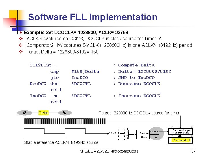
Software FLL Implementation Ø Example: Set DCOCLK= 1228800, ACLK= 32768 v ACLK/4 captured on CCI 2 B, DCOCLK is clock source for Timer_A v Comparator 2 HW captures SMCLK (1228800 Hz) in one ACLK/4 (8192 Hz) period v Target Delta = 1228800/8192= 150 CCI 2 BInt … cmp jlo Dec. DCO dec reti Inc. DCO inc reti #150, Delta Inc. DCO &DCOCTL ; ; &DCOCTL ; Increase DCOCLK Delta Compute Delta= 1228800/8192 JMP to Inc. DCO Decrease DCOCLK Target 1228800 Hz DCOCLK source for timer 15 0 CCI 2 B 1 2 3 Stable reference ACLK/4, 8192 Hz source CPE/EE 421/521 Microcomputers Capture Mode 0 Capture/Compare Register CCR 2 Capture 15 0 Comparator 2 37

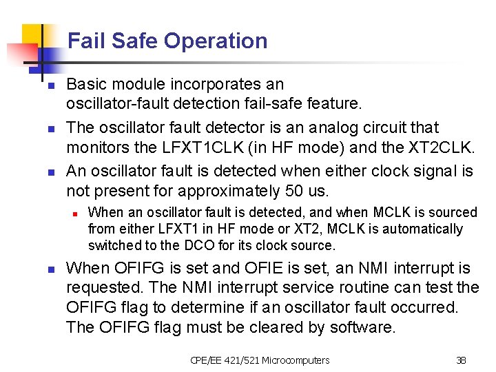
Fail Safe Operation n Basic module incorporates an oscillator-fault detection fail-safe feature. The oscillator fault detector is an analog circuit that monitors the LFXT 1 CLK (in HF mode) and the XT 2 CLK. An oscillator fault is detected when either clock signal is not present for approximately 50 us. n n When an oscillator fault is detected, and when MCLK is sourced from either LFXT 1 in HF mode or XT 2, MCLK is automatically switched to the DCO for its clock source. When OFIFG is set and OFIE is set, an NMI interrupt is requested. The NMI interrupt service routine can test the OFIFG flag to determine if an oscillator fault occurred. The OFIFG flag must be cleared by software. CPE/EE 421/521 Microcomputers 38

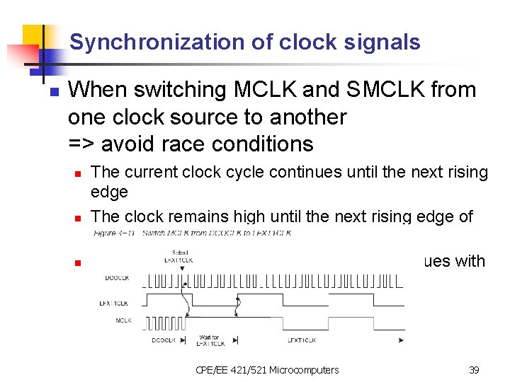
Synchronization of clock signals n When switching MCLK and SMCLK from one clock source to another => avoid race conditions n n n The current clock cycle continues until the next rising edge The clock remains high until the next rising edge of the new clock The new clock source is selected and continues with a full high period CPE/EE 421/521 Microcomputers 39

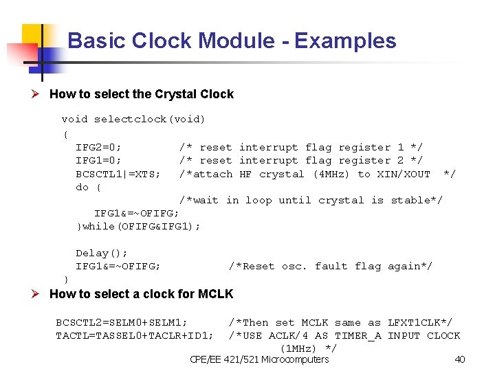
Basic Clock Module - Examples Ø How to select the Crystal Clock void selectclock(void) { IFG 2=0; /* reset interrupt flag register 1 */ IFG 1=0; /* reset interrupt flag register 2 */ BCSCTL 1|=XTS; /*attach HF crystal (4 MHz) to XIN/XOUT */ do { /*wait in loop until crystal is stable*/ IFG 1&=~OFIFG; }while(OFIFG&IFG 1); Delay(); IFG 1&=~OFIFG; /*Reset osc. fault flag again*/ } Ø How to select a clock for MCLK BCSCTL 2=SELM 0+SELM 1; TACTL=TASSEL 0+TACLR+ID 1; /*Then set MCLK same as LFXT 1 CLK*/ /*USE ACLK/4 AS TIMER_A INPUT CLOCK (1 MHz) */ CPE/EE 421/521 Microcomputers 40

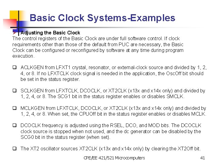
Basic Clock Systems-Examples Ø Adjusting the Basic Clock The control registers of the Basic Clock are under full software control. If clock requirements other than those of the default from PUC are necessary, the Basic Clock can be configured or reconfigured by software at any time during program execution. q ACLKGEN from LFXT 1 crystal, resonator, or external-clock source and divided by 1, 2, 4, or 8. If no LFXTCLK clock signal is needed in the application, the Osc. Off bit should be set in the status register. q SCLKGEN from LFXTCLK, DCOCLK, or XT 2 CLK (x 13 x and x 14 x only) and divided by 1, 2, 4, or 8. The SCG 1 bit in the status register enables or disables SMCLK. q MCLKGEN from LFXTCLK, DCOCLK, or XT 2 CLK (x 13 x and x 14 x only) and divided by 1, 2, 4, or 8. When set, the CPUOff bit in the status register enables or disables MCLK. q DCOCLK frequency is adjusted using the RSEL, DCO, and MOD bits. The DCOCLK clock source is stopped when not used, and the dc generator can be disabled by the SCG 0 bit in the status register (when set). q The XT 2 oscillator sources XT 2 CLK (x 13 x and x 14 x only) by clearing the XT 2 Off bit. CPE/EE 421/521 Microcomputers 41

MSP 430: Watchdog Timer CPE/EE 421/521 Microcomputers

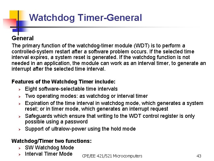
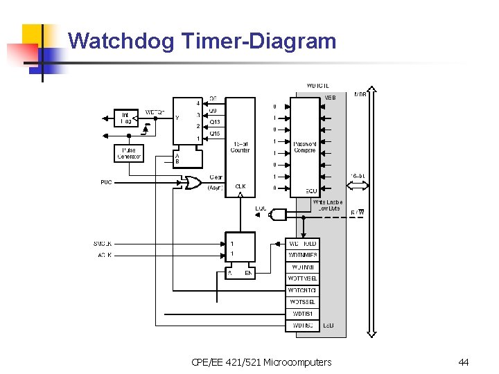
Watchdog Timer-General The primary function of the watchdog-timer module (WDT) is to perform a controlled-system restart after a software problem occurs. If the selected time interval expires, a system reset is generated. If the watchdog function is not needed in an application, the module can work as an interval timer, to generate an interrupt after the selected time interval. Features of the Watchdog Timer include: Ø Eight software-selectable time intervals Ø Two operating modes: as watchdog or interval timer Ø Expiration of the time interval in watchdog mode, which generates a system reset; or in timer mode, which generates an interrupt request Ø Safeguards which ensure that writing to the WDT control register is only possible using a password Ø Support of ultralow-power using the hold mode Watchdog/Timer two functions: Ø SW Watchdog Mode Ø Interval Timer Mode CPE/EE 421/521 Microcomputers 43

Watchdog Timer-Diagram CPE/EE 421/521 Microcomputers 44

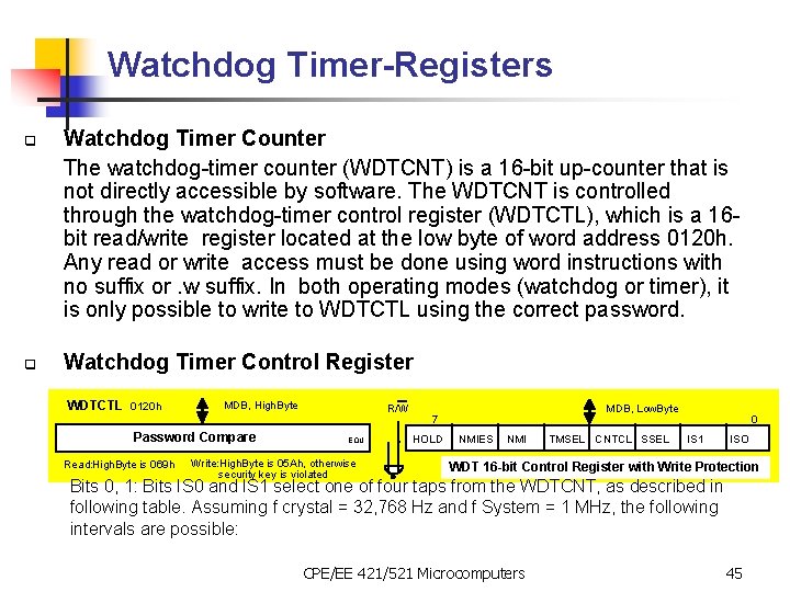
Watchdog Timer-Registers q q Watchdog Timer Counter The watchdog-timer counter (WDTCNT) is a 16 -bit up-counter that is not directly accessible by software. The WDTCNT is controlled through the watchdog-timer control register (WDTCTL), which is a 16 bit read/write register located at the low byte of word address 0120 h. Any read or write access must be done using word instructions with no suffix or. w suffix. In both operating modes (watchdog or timer), it is only possible to write to WDTCTL using the correct password. Watchdog Timer Control Register WDTCTL 0120 h MDB, High. Byte Password Compare Read: High. Byte is 069 h R/W EQU Write: High. Byte is 05 Ah, otherwise security key is violated MDB, Low. Byte 7 HOLD NMIES NMI TMSEL CNTCL SSEL 0 IS 1 ISO WDT 16 -bit Control Register with Write Protection Bits 0, 1: Bits IS 0 and IS 1 select one of four taps from the WDTCNT, as described in following table. Assuming f crystal = 32, 768 Hz and f System = 1 MHz, the following intervals are possible: CPE/EE 421/521 Microcomputers 45

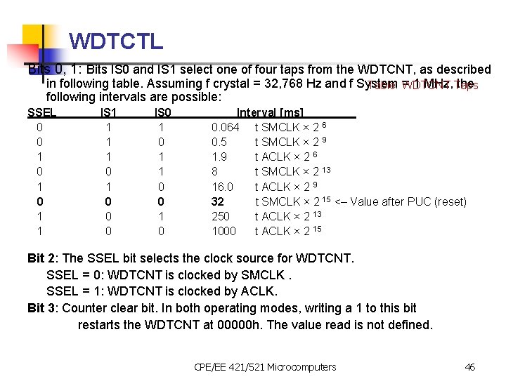
WDTCTL Bits 0, 1: Bits IS 0 and IS 1 select one of four taps from the WDTCNT, as described in following table. Assuming f crystal = 32, 768 Hz and f System = 1 MHz, Taps the Table: WDTCNT following intervals are possible: SSEL 0 0 1 0 1 1 IS 1 1 0 1 0 0 0 IS 0 1 1 0 0 1 0 Interval [ms] 0. 064 t SMCLK × 2 6 0. 5 t SMCLK × 2 9 1. 9 t ACLK × 2 6 8 t SMCLK × 2 13 16. 0 t ACLK × 2 9 32 t SMCLK × 2 15 <– Value after PUC (reset) 250 t ACLK × 2 13 1000 t ACLK × 2 15 Bit 2: The SSEL bit selects the clock source for WDTCNT. SSEL = 0: WDTCNT is clocked by SMCLK. SSEL = 1: WDTCNT is clocked by ACLK. Bit 3: Counter clear bit. In both operating modes, writing a 1 to this bit restarts the WDTCNT at 00000 h. The value read is not defined. CPE/EE 421/521 Microcomputers 46

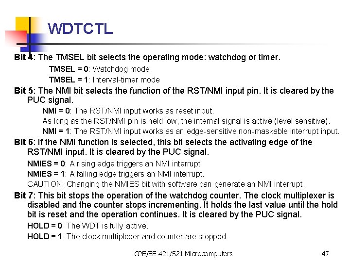
WDTCTL Bit 4: The TMSEL bit selects the operating mode: watchdog or timer. TMSEL = 0: Watchdog mode TMSEL = 1: Interval-timer mode Bit 5: The NMI bit selects the function of the RST/NMI input pin. It is cleared by the PUC signal. NMI = 0: The RST/NMI input works as reset input. As long as the RST/NMI pin is held low, the internal signal is active (level sensitive). NMI = 1: The RST/NMI input works as an edge-sensitive non-maskable interrupt input. Bit 6: If the NMI function is selected, this bit selects the activating edge of the RST/NMI input. It is cleared by the PUC signal. NMIES = 0: A rising edge triggers an NMI interrupt. NMIES = 1: A falling edge triggers an NMI interrupt. CAUTION: Changing the NMIES bit with software can generate an NMI interrupt. Bit 7: This bit stops the operation of the watchdog counter. The clock multiplexer is disabled and the counter stops incrementing. It holds the last value until the hold bit is reset and the operation continues. It is cleared by the PUC signal. HOLD = 0: The WDT is fully active. HOLD = 1: The clock multiplexer and counter are stopped. CPE/EE 421/521 Microcomputers 47

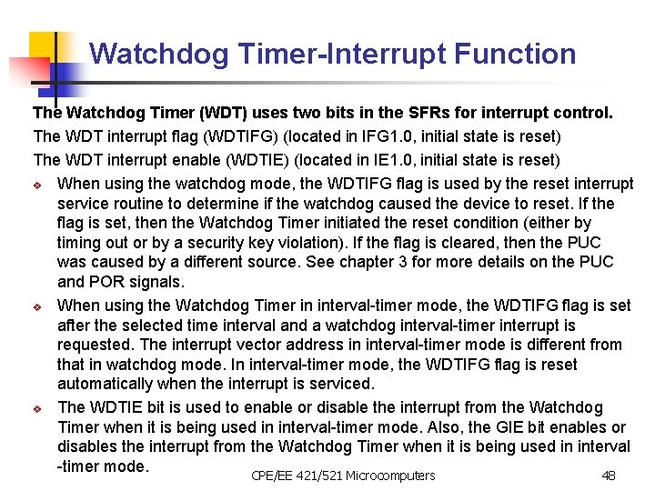
Watchdog Timer-Interrupt Function The Watchdog Timer (WDT) uses two bits in the SFRs for interrupt control. The WDT interrupt flag (WDTIFG) (located in IFG 1. 0, initial state is reset) The WDT interrupt enable (WDTIE) (located in IE 1. 0, initial state is reset) v When using the watchdog mode, the WDTIFG flag is used by the reset interrupt service routine to determine if the watchdog caused the device to reset. If the flag is set, then the Watchdog Timer initiated the reset condition (either by timing out or by a security key violation). If the flag is cleared, then the PUC was caused by a different source. See chapter 3 for more details on the PUC and POR signals. v When using the Watchdog Timer in interval-timer mode, the WDTIFG flag is set after the selected time interval and a watchdog interval-timer interrupt is requested. The interrupt vector address in interval-timer mode is different from that in watchdog mode. In interval-timer mode, the WDTIFG flag is reset automatically when the interrupt is serviced. v The WDTIE bit is used to enable or disable the interrupt from the Watchdog Timer when it is being used in interval-timer mode. Also, the GIE bit enables or disables the interrupt from the Watchdog Timer when it is being used in interval -timer mode. CPE/EE 421/521 Microcomputers 48

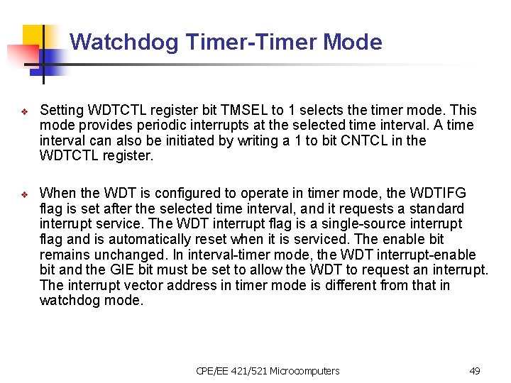
Watchdog Timer-Timer Mode v v Setting WDTCTL register bit TMSEL to 1 selects the timer mode. This mode provides periodic interrupts at the selected time interval. A time interval can also be initiated by writing a 1 to bit CNTCL in the WDTCTL register. When the WDT is configured to operate in timer mode, the WDTIFG flag is set after the selected time interval, and it requests a standard interrupt service. The WDT interrupt flag is a single-source interrupt flag and is automatically reset when it is serviced. The enable bit remains unchanged. In interval-timer mode, the WDT interrupt-enable bit and the GIE bit must be set to allow the WDT to request an interrupt. The interrupt vector address in timer mode is different from that in watchdog mode. CPE/EE 421/521 Microcomputers 49

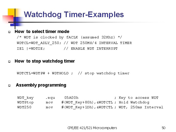
Watchdog Timer-Examples q How to select timer mode /* WDT is clocked by f. ACLK (assumed 32 Khz) */ WDTCL=WDT_ADLY_250; // WDT 250 MS/4 INTERVAL TIMER IE 1 |=WDTIE; // ENABLE WDT INTERRUPT q How to stop watchdog timer WDTCTL=WDTPW + WDTHOLD ; q // stop watchdog timer Assembly programming WDT_key WDTStop WDT 250 . equ mov 05 A 00 h ; Key to access WDT #(WDT_Key+80 h), &WDTCTL ; Hold Watchdog #(WDT_Key+1 Dh), &WDTCTL ; WDT, 250 ms Interval CPE/EE 421/521 Microcomputers 50

MSP 430 x 1 xx Microcontrollers Low Power Modes CPE/EE 421/521 Microcomputers

Power as a Design Constraint Power becomes a first class architectural design constraint n Why worry about power? n n Battery life in portable and mobile platforms Power consumption in desktops, server farms n n n Cooling costs, packaging costs, reliability, timing Power density: 30 W/cm 2 in Alpha 21364 (3 x of typical hot plate) Environment? n IT consumes 10% of energy in the US CPE/EE 421/521 Microcomputers 52

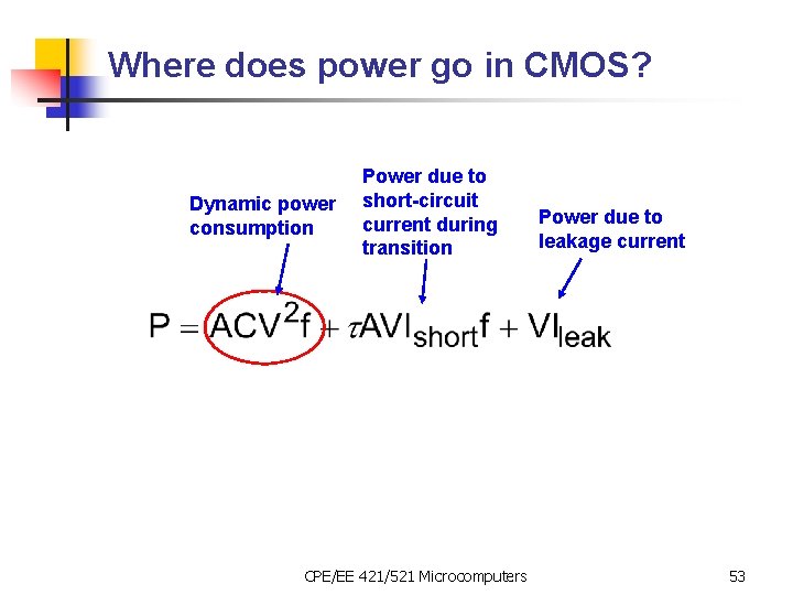
Where does power go in CMOS? Dynamic power consumption Power due to short-circuit current during transition CPE/EE 421/521 Microcomputers Power due to leakage current 53

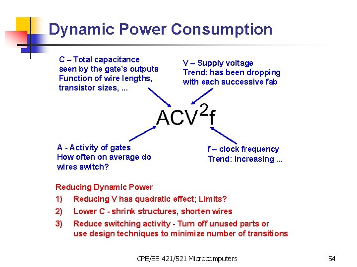
Dynamic Power Consumption C – Total capacitance seen by the gate’s outputs Function of wire lengths, transistor sizes, . . . A - Activity of gates How often on average do wires switch? V – Supply voltage Trend: has been dropping with each successive fab f – clock frequency Trend: increasing. . . Reducing Dynamic Power 1) Reducing V has quadratic effect; Limits? 2) Lower C - shrink structures, shorten wires 3) Reduce switching activity - Turn off unused parts or use design techniques to minimize number of transitions CPE/EE 421/521 Microcomputers 54

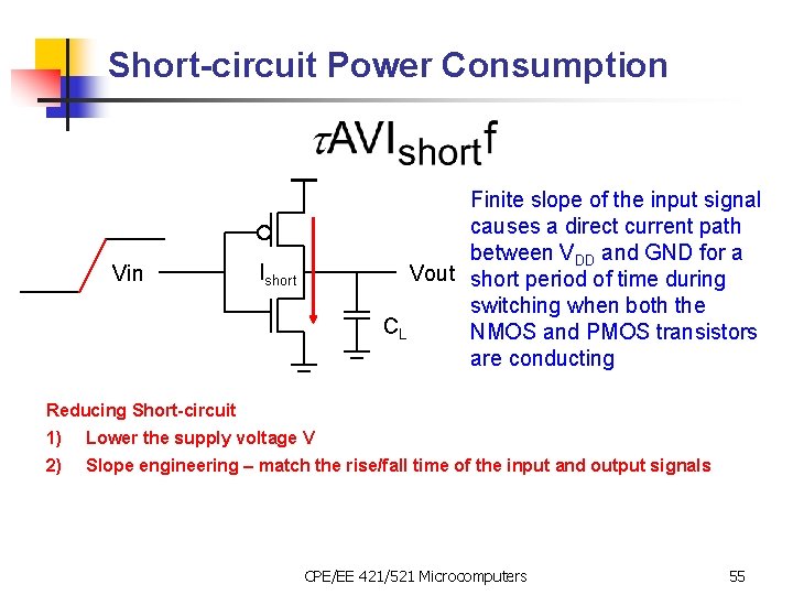
Short-circuit Power Consumption Vin Finite slope of the input signal causes a direct current path between VDD and GND for a Vout short period of time during switching when both the CL NMOS and PMOS transistors are conducting Ishort Reducing Short-circuit 1) Lower the supply voltage V 2) Slope engineering – match the rise/fall time of the input and output signals CPE/EE 421/521 Microcomputers 55

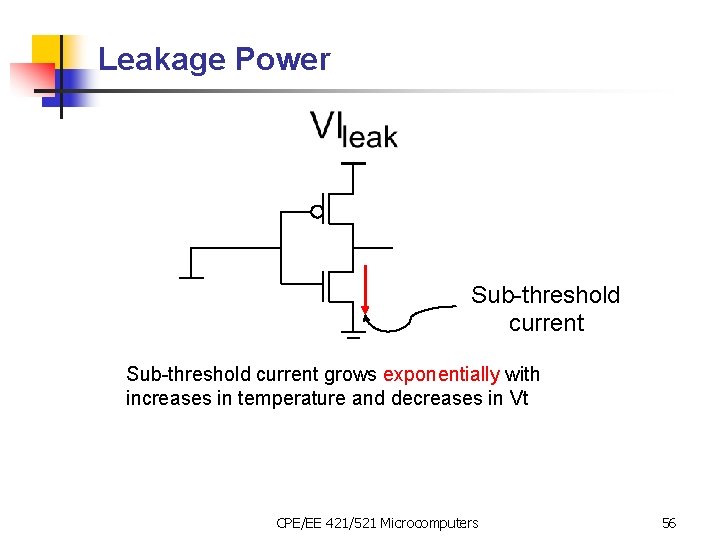
Leakage Power Sub-threshold current grows exponentially with increases in temperature and decreases in Vt CPE/EE 421/521 Microcomputers 56

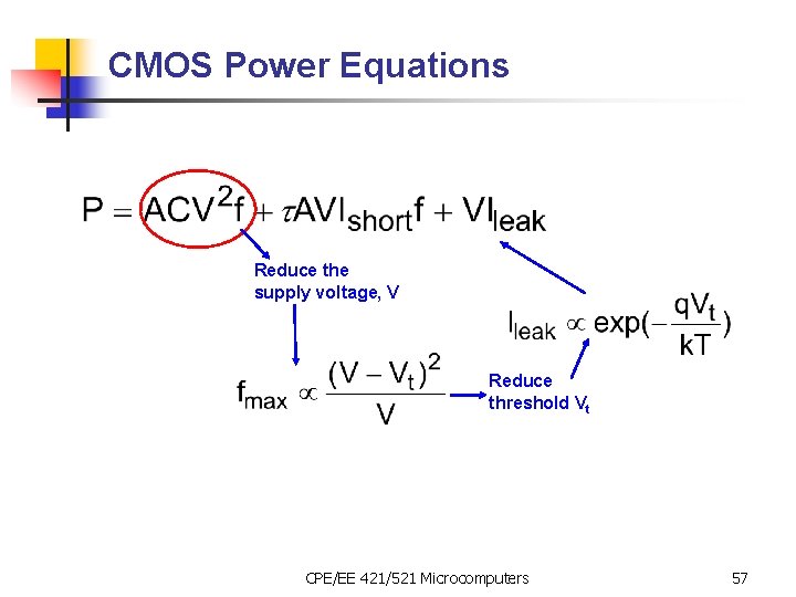
CMOS Power Equations Reduce the supply voltage, V Reduce threshold Vt CPE/EE 421/521 Microcomputers 57

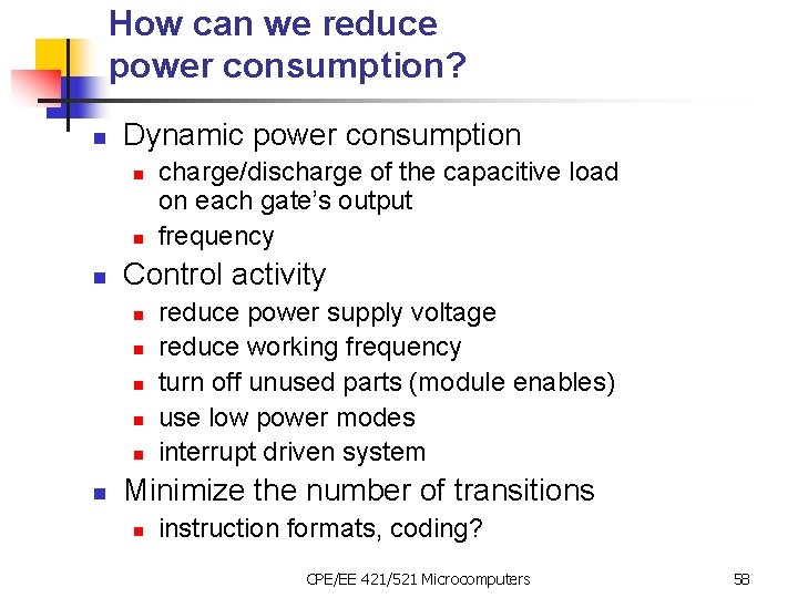
How can we reduce power consumption? n Dynamic power consumption n Control activity n n n charge/discharge of the capacitive load on each gate’s output frequency reduce power supply voltage reduce working frequency turn off unused parts (module enables) use low power modes interrupt driven system Minimize the number of transitions n instruction formats, coding? CPE/EE 421/521 Microcomputers 58

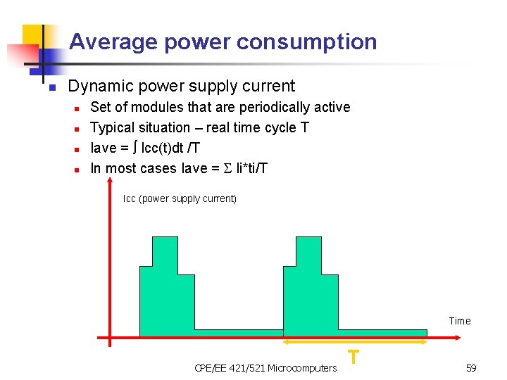
Average power consumption n Dynamic power supply current n n Set of modules that are periodically active Typical situation – real time cycle T Iave = Icc(t)dt /T In most cases Iave = Ii*ti/T Icc (power supply current) Time CPE/EE 421/521 Microcomputers T 59

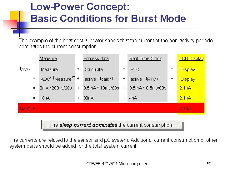
Low-Power Concept: Basic Conditions for Burst Mode The example of the heat cost allocator shows that the current of the non-activity periode dominates the current consumption. Measure IAVG = IMeasure Process data + ICalculate = IADC* t Measure/T + Iactive * tcalc /T Real-Time Clock LCD Display + IRTC + IDisplay + Iactive * t. RTC /T + IDisplay = 3 m. A *200µs/60 s + 0. 5 m. A * 10 ms/60 s + 0. 5 m. A * 0. 5 ms/60 s + 2. 1µA = 10 n. A + 83 n. A + 2. 1µA + 4 n. A IAVG @ 2. 1µA The sleep current dominates the current consumption! The currents are related to the sensor and C system. Additional current consumption of other system parts should be added for the total system current CPE/EE 421/521 Microcomputers 60
![Battery Life n n Battery Capacity BC m Ah Battery Life n n Battery Life n n Battery Capacity BC – [m. Ah] Battery Life n n](https://slidetodoc.com/presentation_image/25b7e96897c3c89f14371366745f5905/image-61.jpg)
Battery Life n n Battery Capacity BC – [m. Ah] Battery Life n n In the previous example, standard 800 m. Ah batteries will allow battery life of: n n BL = BC / Iave BL = 750 m. Ah / 2. 1 A 44 years !!! Conclusion: n n Power efficient modes Interrupt driven system with processor in idle mode CPE/EE 421/521 Microcomputers 61

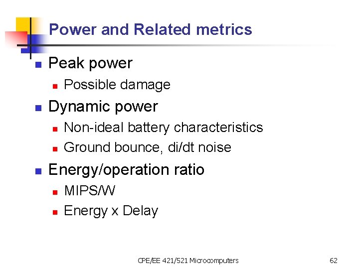
Power and Related metrics n Peak power n n Dynamic power n n n Possible damage Non-ideal battery characteristics Ground bounce, di/dt noise Energy/operation ratio n n MIPS/W Energy x Delay CPE/EE 421/521 Microcomputers 62

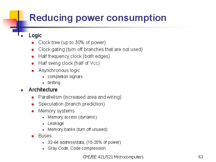
Reducing power consumption n Logic n n n Clock tree (up to 30% of power) Clock gating (turn off branches that are not used) Half frequency clock (both edges) Half swing clock (half of Vcc) Asynchronous logic n n n completion signals testing Architecture n n n Parallelism (increased area and wiring) Speculation (branch prediction) Memory systems n n Memory access (dynamic) Leakage Memory banks (turn off unused) Buses n n 32 -64 address/data, (15 -20% of power) Gray Code, Code compression CPE/EE 421/521 Microcomputers 63

Reducing power consumption #2 n Operating System n n Finish computation “when necessary” Scale the voltage n n n System Architecture n n n Power efficient and specialized processing cores A “convergent” architecture Trade-off n n Application driven Automatic AMD K 6 / 400 MHz / 64 KB cache – 12 W XScale with the same cache 450 m. W @ 600 MHz (40 m. W@150 MHz) 24 processors? Parallelism? Other issues n n Leakage current – Thermal runaway Voltage clustering (low Vthreshold for high speed paths) CPE/EE 421/521 Microcomputers 64

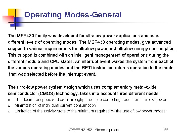
Operating Modes-General The MSP 430 family was developed for ultralow-power applications and uses different levels of operating modes. The MSP 430 operating modes, give advanced support to various requirements for ultralow power and ultralow energy consumption. This support is combined with an intelligent management of operations during the different module and CPU states. An interrupt event wakes the system from each of the various operating modes and the RETI instruction returns operation to the mode that was selected before the interrupt event. The ultra-low power system design which uses complementary metal-oxide semiconductor (CMOS) technology, takes into account three different needs: q q q The desire for speed and data throughput despite conflicting needs for ultra-low power Minimization of individual current consumption Limitation of the activity state to the minimum required by the use of low power modes CPE/EE 421/521 Microcomputers 65

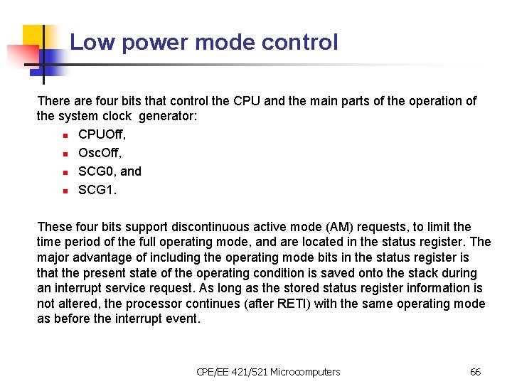
Low power mode control There are four bits that control the CPU and the main parts of the operation of the system clock generator: n CPUOff, n Osc. Off, n SCG 0, and n SCG 1. These four bits support discontinuous active mode (AM) requests, to limit the time period of the full operating mode, and are located in the status register. The major advantage of including the operating mode bits in the status register is that the present state of the operating condition is saved onto the stack during an interrupt service request. As long as the stored status register information is not altered, the processor continues (after RETI) with the same operating mode as before the interrupt event. CPE/EE 421/521 Microcomputers 66

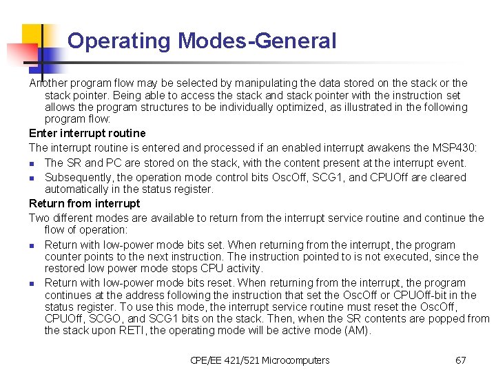
Operating Modes-General Another program flow may be selected by manipulating the data stored on the stack or the stack pointer. Being able to access the stack and stack pointer with the instruction set allows the program structures to be individually optimized, as illustrated in the following program flow: Enter interrupt routine The interrupt routine is entered and processed if an enabled interrupt awakens the MSP 430: n The SR and PC are stored on the stack, with the content present at the interrupt event. n Subsequently, the operation mode control bits Osc. Off, SCG 1, and CPUOff are cleared automatically in the status register. Return from interrupt Two different modes are available to return from the interrupt service routine and continue the flow of operation: n Return with low-power mode bits set. When returning from the interrupt, the program counter points to the next instruction. The instruction pointed to is not executed, since the restored low power mode stops CPU activity. n Return with low-power mode bits reset. When returning from the interrupt, the program continues at the address following the instruction that set the Osc. Off or CPUOff-bit in the status register. To use this mode, the interrupt service routine must reset the Osc. Off, CPUOff, SCGO, and SCG 1 bits on the stack. Then, when the SR contents are popped from the stack upon RETI, the operating mode will be active mode (AM). CPE/EE 421/521 Microcomputers 67

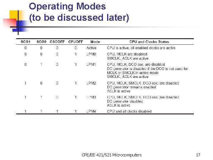
Operating Modes – Software configurable There are six operating modes that the software can configure: q Active mode AM; SCG 1=0, SCG 0=0, Osc. Off=0, CPUOff=0: CPU clocks are active q Low power mode 0 (LPM 0); SCG 1=0, SCG 0=0, Osc. Off=0, CPUOff=1: n n n q Low power mode 1 (LPM 1); SCG 1=0, SCG 0=1, Osc. Off=0, CPUOff=1: n n q CPU is disabled MCLK is disabled SMCLK and ACLK remain active CPU is disabled MCLK is disabled DCO’s dc generator is disabled if the DCO is not used for MCLK or SMCLK when in active mode. Otherwise, it remains enabled. SMCLK and ACLK remain active Low power mode 2 (LPM 2); SCG 1=1, SCG 0=0, Osc. Off=0, CPUOff=1: n n n CPU is disabled MCLK is disabled SMCLK is disabled DCO oscillator automatically disabled because it is not needed for MCLK or SMCLK DCO’s dc-generator remains enabled ACLK remains active CPE/EE 421/521 Microcomputers 68

Operating Modes #2 q Low power mode 3 (LPM 3); SCG 1=1, SCG 0=1, Osc. Off=0, CPUOff=1: n n n q CPU is disabled MCLK is disabled SMCLK is disabled DCO oscillator is disabled DCO’s dc-generator is disabled ACLK remains active Low power mode 4 (LPM 4); SCG 1=X, SCG 0=X, Osc. Off=1, CPUOff=1: n n n n CPU is disabled ACLK is disabled MCLK is disabled SMCLK is disabled DCO oscillator is disabled DCO’s dc-generator is disabled Crystal oscillator is stopped CPE/EE 421/521 Microcomputers 69

Operating Modes-Low Power Mode in details Low-Power Mode 0 and 1 (LPM 0 and LPM 1) Low power mode 0 or 1 is selected if bit CPUOff in the status register is set. Immediately after the bit is set the CPU stops operation, and the normal operation of the system core stops. The operation of the CPU halts and all internal bus activities stop until an interrupt request or reset occurs. The system clock generator continues operation, and the clock signals MCLK, SMCLK, and ACLK stay active depending on the state of the other three status register bits, SCG 0, SCG 1, and Osc. Off. 1. The peripherals are enabled or disabled with their individual control register settings, and with the module enable registers in the SFRs. All I/O port pins and RAM/registers are unchanged. Wake up is possible through all enabled interrupts. Low-Power Modes 2 and 3 (LPM 2 and LPM 3) Low-power mode 2 or 3 is selected if bits CPUOff and SCG 1 in the status register are set. Immediately after the bits are set, CPU, MCLK, and SMCLK operations halt and all internal bus activities stop until an interrupt request or reset occurs. 1. Peripherals that operate with the MCLK or SMCLK signal are inactive because the clock signals are inactive. Peripherals that operate with the ACLK signal are active or inactive according with the individual control registers and the module enable bits in the SFRs. All I/O port pins and the RAM/registers are unchanged. Wake up is possible by enabled interrupts coming from active peripherals or RST/NMI. CPE/EE 421/521 Microcomputers 70

Operating Modes Low Power Mode in details Low-Power Mode 4 (LPM 4) System Resets, Interrupts, and Operating Modes In low power mode 4 all activities cease; only the RAM contents, I/O ports, and registers are maintained. Wake up is only possible by enabled external interrupts. q Before activating LPM 4, the software should consider the system conditions during the low power mode period. The two most important conditions are environmental (that is, temperature effect on the DCO), and the clocked operation conditions. The environment defines whether the value of the frequency integrator should be held or corrected. A correction should be made when ambient conditions are anticipated to change drastically enough to increase or decrease the system frequency while the device is in LPM 4. CPE/EE 421/521 Microcomputers 71

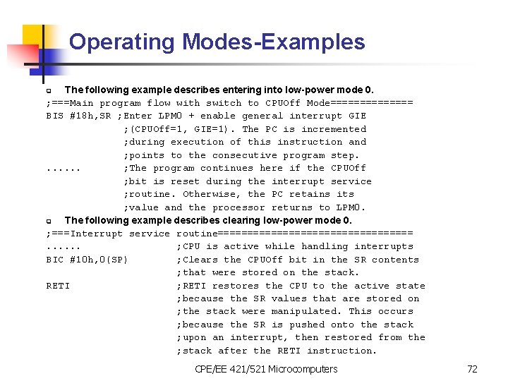
Operating Modes-Examples The following example describes entering into low-power mode 0. ; ===Main program flow with switch to CPUOff Mode======= BIS #18 h, SR ; Enter LPM 0 + enable general interrupt GIE ; (CPUOff=1, GIE=1). The PC is incremented ; during execution of this instruction and ; points to the consecutive program step. . . . ; The program continues here if the CPUOff ; bit is reset during the interrupt service ; routine. Otherwise, the PC retains its ; value and the processor returns to LPM 0. q The following example describes clearing low-power mode 0. ; ===Interrupt service routine=================. . . ; CPU is active while handling interrupts BIC #10 h, 0(SP) ; Clears the CPUOff bit in the SR contents ; that were stored on the stack. RETI ; RETI restores the CPU to the active state ; because the SR values that are stored on ; the stack were manipulated. This occurs ; because the SR is pushed onto the stack ; upon an interrupt, then restored from the ; stack after the RETI instruction. q CPE/EE 421/521 Microcomputers 72

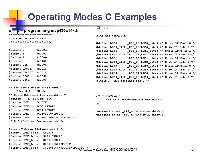
Operating Modes C Examples q q … C – programming msp 430 x 14 x. h /************ * STATUS REGISTER BITS ************/ #define #define #define C Z N V GIE CPUOFF OSCOFF SCG 0 SCG 1 #include "In 430. h“ #define LPM 0 _BIS_SR(LPM 0_bits) #define LPM 0_EXIT _BIC_SR(LPM 0_bits) #define LPM 1 _BIS_SR(LPM 1_bits) #define LPM 1_EXIT _BIC_SR(LPM 1_bits) #define LPM 2 _BIS_SR(LPM 2_bits) #define LPM 2_EXIT _BIC_SR(LPM 2_bits) #define LPM 3 _BIS_SR(LPM 3_bits) #define LPM 3_EXIT _BIC_SR(LPM 3_bits) #define LPM 4 _BIS_SR(LPM 4_bits) #define LPM 4_EXIT _BIC_SR(LPM 4_bits) #endif /* End #defines for C */ 0 x 0001 0 x 0002 0 x 0004 0 x 0100 0 x 0008 0 x 0010 0 x 0020 0 x 0040 0 x 0080 /* Low Power Modes coded with Bits 4 -7 in SR */ /* Begin #defines for assembler */ #ifndef __IAR_SYSTEMS_ICC #define LPM 0 CPUOFF #define LPM 1 SCG 0+CPUOFF #define LPM 2 SCG 1+CPUOFF #define LPM 3 SCG 1+SCG 0+CPUOFF #define LPM 4 SCG 1+SCG 0+OSCOFF+CPUOFF /* End #defines for assembler */ /* /* /* Enter LP Mode 0 */ Exit LP Mode 0 */ Enter LP Mode 1 */ Exit LP Mode 1 */ Enter LP Mode 2 */ Exit LP Mode 2 */ Enter LP Mode 3 */ Exit LP Mode 3 */ Enter LP Mode 4 */ Exit LP Mode 4 */ /* - in 430. h Intrinsic functions for the MSP 430 */ unsigned short _BIS_SR(unsigned short); unsigned short _BIC_SR(unsigned short); #else /* Begin #defines for C */ #define LPM 0_bits CPUOFF #define LPM 1_bits SCG 0+CPUOFF #define LPM 2_bits SCG 1+CPUOFF #define LPM 3_bits SCG 1+SCG 0+CPUOFF #define LPM 4_bits SCG 1+SCG 0+OSCOFF+CPUOFF CPE/EE 421/521 Microcomputers 73

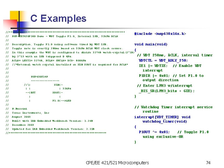
C Examples //*********************************** #include <msp 430 x 14 x. h> // MSP-FET 430 P 140 Demo - WDT Toggle P 1. 0, Interval ISR, 32 k. Hz ACLK // // Description; Toggle P 1. 0 using software timed by WDT ISR. void main(void) // Toggle rate is exactly 250 ms based on 32 k. Hz ACLK WDT clock source. { // In this example the WDT is configured to divide 32768 watch-crystal(2^15) // WDT 250 ms, ACLK, interval timer // by 2^13 with an ISR triggered @ 4 Hz. // ACLK= LFXT 1= 32768, MCLK= SMCLK= DCO~ 800 k. Hz WDTCTL = WDT_ADLY_250; // //*External watch crystal installed on XIN XOUT is required for ACLK* IE 1 |= WDTIE; // Enable WDT // interrupt // P 1 DIR |= 0 x 01; // Set P 1. 0 to // MSP 430 F 149 output direction // --------// /|| XIN|// Enter LPM 3 w/interrupt // | | | 32 k. Hz _BIS_SR(LPM 3_bits + GIE); // --|RST XOUT|} // | | // | P 1. 0|-->LED // // Watchdog Timer interrupt service // M. Buccini routine // Texas Instruments, Inc // August 2003 interrupt[WDT_TIMER] void // Built with IAR Embedded Workbench Version: 1. 26 B watchdog_timer(void) // December 2003 { // Updated for IAR Embedded Workbench Version: 2. 21 B P 1 OUT ^= 0 x 01; // Toggle P 1. 0 //***************************** using exclusive-OR } CPE/EE 421/521 Microcomputers 74

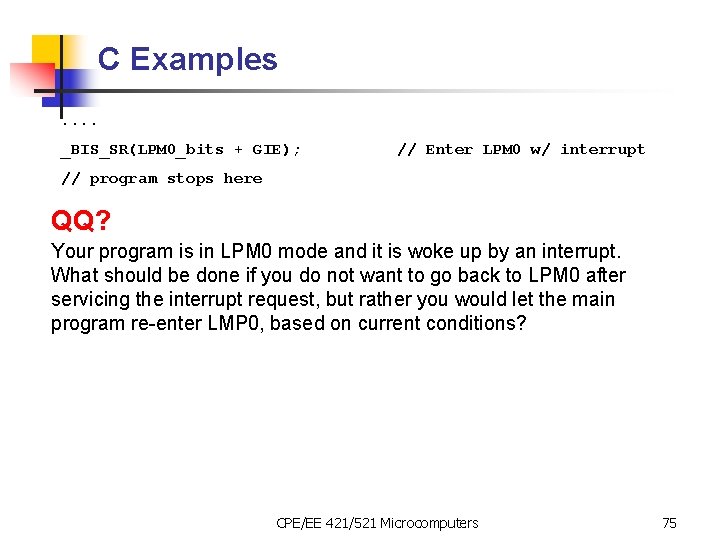
C Examples. . _BIS_SR(LPM 0_bits + GIE); // Enter LPM 0 w/ interrupt // program stops here QQ? Your program is in LPM 0 mode and it is woke up by an interrupt. What should be done if you do not want to go back to LPM 0 after servicing the interrupt request, but rather you would let the main program re-enter LMP 0, based on current conditions? CPE/EE 421/521 Microcomputers 75

MSP 430: Digital I/O CPE/EE 421/521 Microcomputers

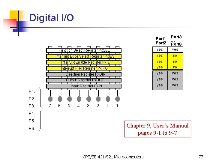
Digital I/O Port 1 Port 2 Port 3 … Port 6 Function Select Register Px. SEL yes Interrupt Edge Select Register Px. IES yes no Interrupt Enable Register Px. IE yes no Interrupt Flag Register Px. IFG yes no Direction Register Px. DIR yes Output Register Px. OUT yes yes Input Register Px. IN P 1. P 2. P 3. 7 6 5 4 3 2 1 0 P 4. P 5. P 6. Chapter 9, User’s Manual pages 9 -1 to 9 -7 CPE/EE 421/521 Microcomputers 77

Digital I/O Introduction n n MSP 430 family – up to 6 digital I/O ports implemented, P 1 -P 6 MSP 430 F 14 x – all 6 ports implemented Ports P 1 and P 2 have interrupt capability. Each interrupt for the P 1 and P 2 I/O lines can be individually enabled and configured to provide an interrupt on a rising edge or falling edge of an input signal. The digital I/O features include: n n n Independently programmable individual I/Os Any combination of input or output Individually configurable P 1 and P 2 interrupts Independent input and output data registers The digital I/O is configured with user software CPE/EE 421/521 Microcomputers 78

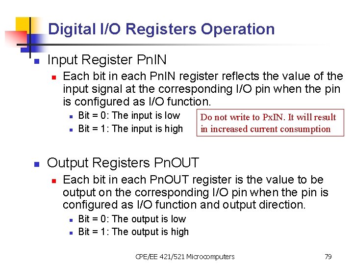
Digital I/O Registers Operation n Input Register Pn. IN n Each bit in each Pn. IN register reflects the value of the input signal at the corresponding I/O pin when the pin is configured as I/O function. n n n Bit = 0: The input is low Bit = 1: The input is high Do not write to Px. IN. It will result in increased current consumption Output Registers Pn. OUT n Each bit in each Pn. OUT register is the value to be output on the corresponding I/O pin when the pin is configured as I/O function and output direction. n n Bit = 0: The output is low Bit = 1: The output is high CPE/EE 421/521 Microcomputers 79

Digital I/O Operation n Direction Registers Pn. DIR n n n Bit = 0: The port pin is switched to input direction Bit = 1: The port pin is switched to output direction Function Select Registers Pn. SEL n Port pins are often multiplexed with other peripheral module functions. n n Bit = 0: I/O Function is selected for the pin Bit = 1: Peripheral module function is selected for the pin CPE/EE 421/521 Microcomputers 80

Digital I/O Operation n Interrupt Flag Registers P 1 IFG, P 2 IFG (only for P 1 and P 2) n n Only transitions, not static levels, cause interrupts Interrupt Edge Select Registers P 1 IES, P 2 IES n n Bit = 0: No interrupt is pending Bit = 1: An interrupt is pending (only for P 1 and P 2) Each Pn. IES bit selects the interrupt edge for the corresponding I/O pin. n n Bit = 0: The Pn. IFGx flag is set with a low-to-high transition Bit = 1: The Pn. IFGx flag is set with a high-to-low transition CPE/EE 421/521 Microcomputers 81

MSP 430: Timer_A CPE/EE 421/521 Microcomputers

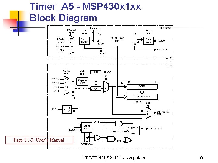
Timer_A MSP 430 x 1 xx n n n 16 -bit counter with 4 operating modes Selectable and configurable clock source Three (or five) independently configurable capture/compare registers with configurable inputs Three (or five) individually configurable output modules with 8 output modes multiple, simultaneous, timings; multiple capture/compares; multiple output waveforms such as PWM signals; and any combination of these. Interrupt capabilities n each capture/compare block individually configurable CPE/EE 421/521 Microcomputers 83

Timer_A 5 - MSP 430 x 1 xx Block Diagram Page 11 -3, User’s Manual CPE/EE 421/521 Microcomputers 84

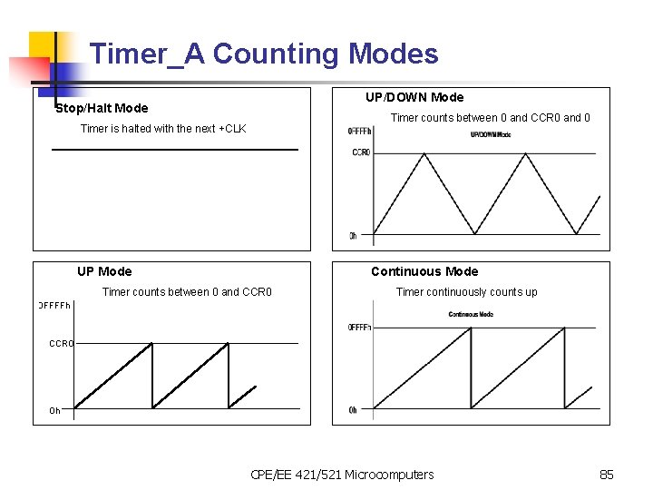
Timer_A Counting Modes UP/DOWN Mode Stop/Halt Mode Timer counts between 0 and CCR 0 and 0 Timer is halted with the next +CLK UP Mode Continuous Mode Timer counts between 0 and CCR 0 Timer continuously counts up 0 FFFFh CCR 0 0 h CPE/EE 421/521 Microcomputers 85

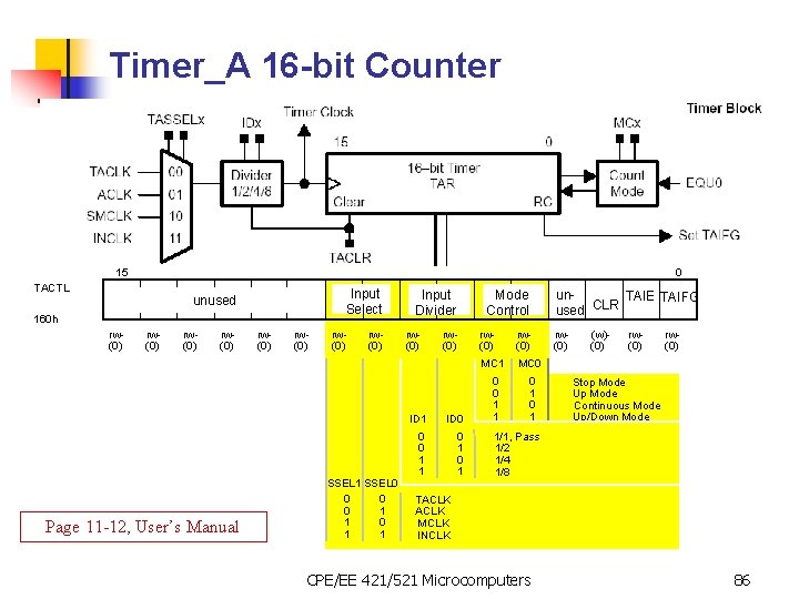
Timer_A 16 -bit Counter 15 0 TACTL Input Select unused 160 h rw(0) Page 11 -12, User’s Manual rw(0) SSEL 1 SSEL 0 0 1 1 Input Divider rw(0) Mode Control rw(0) ID 1 ID 0 0 0 1 1 0 1 un. TAIE TAIFG used CLR rw(0) MC 1 MC 0 0 0 1 1 0 1 rw(0) (w)(0) rw(0) Stop Mode Up Mode Continuous Mode Up/Down Mode 1/1, Pass 1/2 1/4 1/8 TACLK MCLK INCLK CPE/EE 421/521 Microcomputers 86

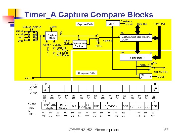
Timer_A Capture Compare Blocks CMPx CCISx 1 CCISx 0 0 CCIx. A 1 CCIx. B 2 GND 3 VCC Timer Clock CCMx 0 0 Disabled 1 Pos. Edge 0 Neg. Edge 1 Both Edges 0 Capture/Compare Register CCRx Capture 0 Synchronize Capture Timer Bus Data Bus 15 1 Capture Mode CCMx 1 0 0 1 1 Overflow x COVx Logic Capture Path SCSx 15 0 Comparator to Port 0 x EQUx 0 1 Compare Path EN A CCIx CCRx 0172 h to 017 Eh CCTLx 162 h to 16 Eh 2 rw(0) CAPTURE MODE rw(0) SCCIx 0 15 rw(0) 15 Set_CCIFGx Y 15 2 CAPx rw(0) INPUT SELECT rw(0) rw(0) SCS SCCI un. CAP used rw(0) rw(0) OUTMODx rw(0) CPE/EE 421/521 Microcomputers rw(0) 0 rw(0) 0 CCIE CCI OUT COV CCIFG rw(0) r rw(0) 87

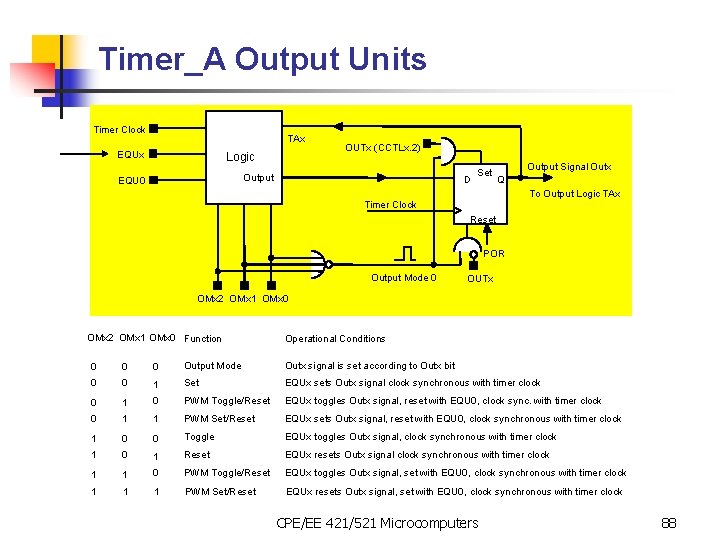
Timer_A Output Units Timer Clock TAx EQUx Logic OUTx (CCTLx. 2) Output EQU 0 D Set Output Signal Outx Q To Output Logic TAx Timer Clock Reset POR Output Mode 0 OUTx OMx 2 OMx 1 OMx 0 Function Operational Conditions 0 0 0 Output Mode Outx signal is set according to Outx bit 0 0 1 Set EQUx sets Outx signal clock synchronous with timer clock 0 1 0 PWM Toggle/Reset EQUx toggles Outx signal, reset with EQU 0, clock sync. with timer clock 0 1 1 PWM Set/Reset EQUx sets Outx signal, reset with EQU 0, clock synchronous with timer clock 1 0 0 Toggle EQUx toggles Outx signal, clock synchronous with timer clock 1 0 1 Reset EQUx resets Outx signal clock synchronous with timer clock 1 1 0 PWM Toggle/Reset EQUx toggles Outx signal, set with EQU 0, clock synchronous with timer clock 1 1 1 PWM Set/Reset EQUx resets Outx signal, set with EQU 0, clock synchronous with timer clock CPE/EE 421/521 Microcomputers 88

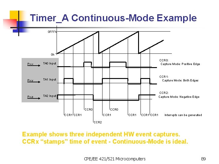
Timer_A Continuous-Mode Example 0 FFFh 0 h Px. x TA 0 Input CCR 0: Capture Mode: Positive Edge Px. y TA 1 Input CCR 1: Capture Mode: Both Edges Px. z TA 2 Input CCR 2: Capture Mode: Negative Edge CCR 0 CCR 1 CCR 1 Interrupts can be generated CCR 2 Example shows three independent HW event captures. CCRx “stamps” time of event - Continuous-Mode is ideal. CPE/EE 421/521 Microcomputers 89

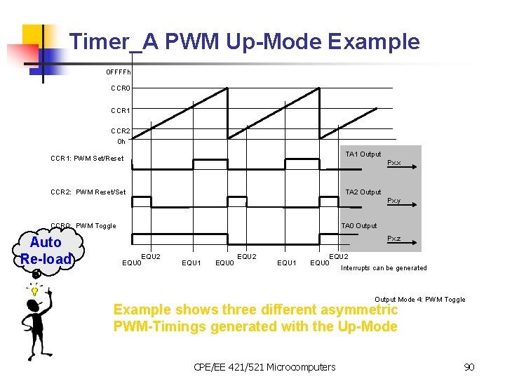
Timer_A PWM Up-Mode Example 0 FFFFh CCR 0 CCR 1 CCR 2 0 h TA 1 Output CCR 1: PWM Set/Reset Px. x CCR 2: PWM Reset/Set TA 2 Output Px. y CCR 0: PWM Toggle Auto Re-load TA 0 Output Px. z EQU 0 EQU 2 EQU 1 EQU 2 EQU 0 Interrupts can be generated Output Mode 4: PWM Toggle Example shows three different asymmetric PWM-Timings generated with the Up-Mode CPE/EE 421/521 Microcomputers 90

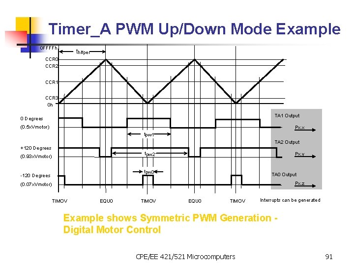
Timer_A PWM Up/Down Mode Example 0 FFFFh thlfper CCR 0 CCR 2 CCR 1 CCR 3 0 h TA 1 Output 0 Degrees (0. 5 x. Vmotor) Px. x tpw 1 TA 2 Output +120 Degrees tpw 2 (0. 93 x. Vmotor) Px. y tpw 3 -120 Degrees TA 0 Output Px. z (0. 07 x. Vmotor) TIMOV EQU 0 TIMOV Interrupts can be generated Example shows Symmetric PWM Generation Digital Motor Control CPE/EE 421/521 Microcomputers 91

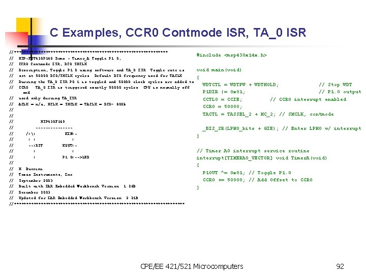
C Examples, CCR 0 Contmode ISR, TA_0 ISR //******************************** // MSP-FET 430 P 140 Demo - Timer_A Toggle P 1. 0, // CCR 0 Contmode ISR, DCO SMCLK // Description; Toggle P 1. 0 using software and TA_0 ISR. Toggle rate is // set at 50000 DCO/SMCLK cycles. Default DCO frequency used for TACLK. // Durring the TA_0 ISR P 0. 1 is toggled and 50000 clock cycles are added to // CCR 0. TA_0 ISR is triggered exactly 50000 cycles. CPU is normally off and // used only durring TA_ISR. // ACLK = n/a, MCLK = SMCLK = TACLK = DCO~ 800 k // // // MSP 430 F 149 // -------// /|| XIN|// | | | // --|RST XOUT|// | | // | P 1. 0|-->LED // // M. Buccini // Texas Instruments, Inc // September 2003 // Built with IAR Embedded Workbench Version: 1. 26 B // December 2003 // Updated for IAR Embedded Workbench Version: 2. 21 B //*********************************** #include <msp 430 x 14 x. h> void main(void) { WDTCTL = WDTPW + WDTHOLD; // Stop WDT P 1 DIR |= 0 x 01; // P 1. 0 output CCTL 0 = CCIE; // CCR 0 interrupt enabled CCR 0 = 50000; TACTL = TASSEL_2 + MC_2; // SMCLK, contmode _BIS_SR(LPM 0_bits + GIE); // Enter LPM 0 w/ interrupt } // Timer A 0 interrupt service routine interrupt[TIMERA 0_VECTOR] void Timer. A(void) { P 1 OUT ^= 0 x 01; // Toggle P 1. 0 CCR 0 += 50000; // Add Offset to CCR 0 } CPE/EE 421/521 Microcomputers 92

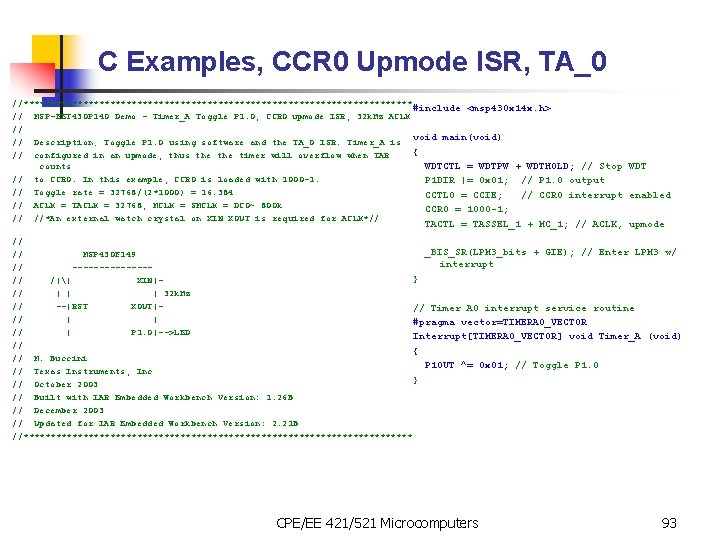
C Examples, CCR 0 Upmode ISR, TA_0 //************************************ #include <msp 430 x 14 x. h> // MSP-FET 430 P 140 Demo - Timer_A Toggle P 1. 0, CCR 0 upmode ISR, 32 k. Hz ACLK // void main(void) // Description; Toggle P 1. 0 using software and the TA_0 ISR. Timer_A is { // configured in an upmode, thus the timer will overflow when TAR counts WDTCTL = WDTPW + WDTHOLD; // Stop WDT // to CCR 0. In this example, CCR 0 is loaded with 1000 -1. P 1 DIR |= 0 x 01; // P 1. 0 output // Toggle rate = 32768/(2*1000) = 16. 384 CCTL 0 = CCIE; // CCR 0 interrupt enabled // ACLK = TACLK = 32768, MCLK = SMCLK = DCO~ 800 k CCR 0 = 1000 -1; // //*An external watch crystal on XIN XOUT is required for ACLK*// TACTL = TASSEL_1 + MC_1; // ACLK, upmode // _BIS_SR(LPM 3_bits + GIE); // Enter LPM 3 w/ // MSP 430 F 149 interrupt // -------} // /|| XIN|// | | | 32 k. Hz // --|RST XOUT|// Timer A 0 interrupt service routine // | | #pragma vector=TIMERA 0_VECTOR // | P 1. 0|-->LED Interrupt[TIMERA 0_VECTOR] void Timer_A (void) // { // M. Buccini P 1 OUT ^= 0 x 01; // Toggle P 1. 0 // Texas Instruments, Inc } // October 2003 // Built with IAR Embedded Workbench Version: 1. 26 B // December 2003 // Updated for IAR Embedded Workbench Version: 2. 21 B //************************************ CPE/EE 421/521 Microcomputers 93

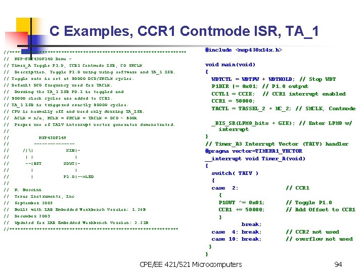
C Examples, CCR 1 Contmode ISR, TA_1 //********************************* // MSP-FET 430 P 140 Demo – // Timer_A Toggle P 1. 0, CCR 1 Contmode ISR, CO SMCLK // Description; Toggle P 1. 0 using software and TA_1 ISR. // Toggle rate is set at 50000 DCO/SMCLK cycles. // Default DCO frequency used for TACLK. // Durring the TA_1 ISR P 0. 1 is toggled and // 50000 clock cycles are added to CCR 1. // TA_1 ISR is triggered exactly 50000 cycles. // CPU is normally off and used only durring TA_ISR. // ACLK = n/a, MCLK = SMCLK = TACLK = DCO ~ 800 k // Proper use of TAIV interrupt vector generator demonstrated. // // MSP 430 F 149 // -------// /|| XIN|// | | | // --|RST XOUT|// | | // | P 1. 0|-->LED // // M. Buccini // Texas Instruments, Inc // September 2003 // Built with IAR Embedded Workbench Version: 1. 26 B // December 2003 // Updated for IAR Embedded Workbench Version: 2. 21 B //******************************* #include <msp 430 x 14 x. h> void main(void) { WDTCTL = WDTPW + WDTHOLD; // Stop WDT P 1 DIR |= 0 x 01; // P 1. 0 output CCTL 1 = CCIE; // CCR 1 interrupt enabled CCR 1 = 50000; TACTL = TASSEL_2 + MC_2; // SMCLK, Contmode _BIS_SR(LPM 0_bits + GIE); // Enter LPM 0 w/ interrupt } // Timer_A 3 Interrupt Vector (TAIV) handler #pragma vector=TIMERA 1_VECTOR __interrupt void Timer_A(void) { switch( TAIV ) { case 2: // CCR 1 { P 1 OUT ^= 0 x 01; // Toggle P 1. 0 CCR 1 += 50000; // Add Offset to CCR 1 } break; case 4: break; // CCR 2 not used case 10: break; // overflow not used } } CPE/EE 421/521 Microcomputers 94

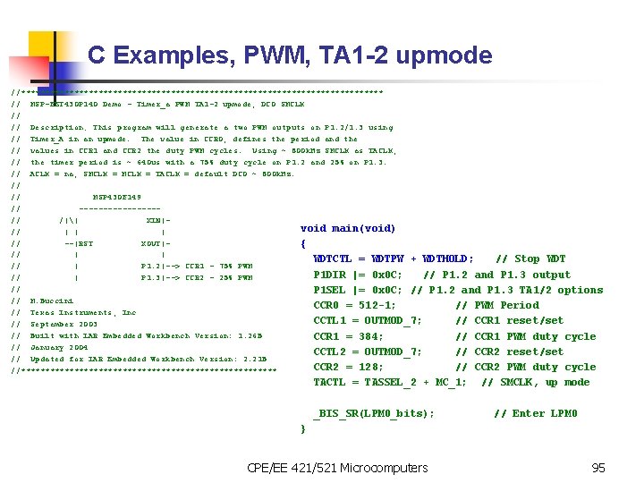
C Examples, PWM, TA 1 -2 upmode //************************************** // MSP-FET 430 P 140 Demo - Timer_a PWM TA 1 -2 upmode, DCO SMCLK // // Description; This program will generate a two PWM outputs on P 1. 2/1. 3 using // Timer_A in an upmode. The value in CCR 0, defines the period and the // values in CCR 1 and CCR 2 the duty PWM cycles. Using ~ 800 k. Hz SMCLK as TACLK, // the timer period is ~ 640 us with a 75% duty cycle on P 1. 2 and 25% on P 1. 3. // ACLK = na, SMCLK = TACLK = default DCO ~ 800 k. Hz. // // MSP 430 F 149 // --------// /|| XIN|void main(void) // | | | // --|RST XOUT|{ // | | WDTCTL = WDTPW + WDTHOLD; // Stop WDT // | P 1. 2|--> CCR 1 - 75% PWM P 1 DIR |= 0 x 0 C; // P 1. 2 and P 1. 3 output // | P 1. 3|--> CCR 2 - 25% PWM // P 1 SEL |= 0 x 0 C; // P 1. 2 and P 1. 3 TA 1/2 options // M. Buccini CCR 0 = 512 -1; // PWM Period // Texas Instruments, Inc CCTL 1 = OUTMOD_7; // CCR 1 reset/set // September 2003 // Built with IAR Embedded Workbench Version: 1. 26 B CCR 1 = 384; // CCR 1 PWM duty cycle // January 2004 CCTL 2 = OUTMOD_7; // CCR 2 reset/set // Updated for IAR Embedded Workbench Version: 2. 21 B CCR 2 = 128; // CCR 2 PWM duty cycle //*************************** TACTL = TASSEL_2 + MC_1; _BIS_SR(LPM 0_bits); // SMCLK, up mode // Enter LPM 0 } CPE/EE 421/521 Microcomputers 95

Serial Communication CPE/EE 421/521 Microcomputers

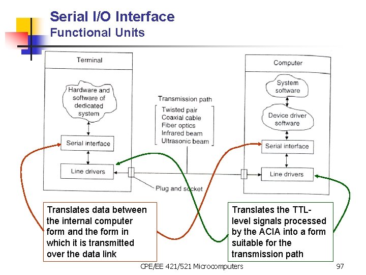
Serial I/O Interface Functional Units Translates data between the internal computer form and the form in which it is transmitted over the data link Translates the TTLlevel signals processed by the ACIA into a form suitable for the transmission path CPE/EE 421/521 Microcomputers 97

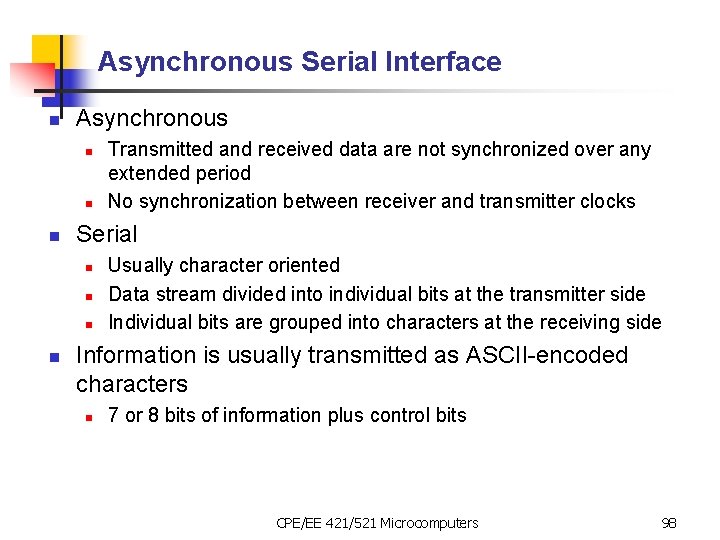
Asynchronous Serial Interface n Asynchronous n n n Serial n n Transmitted and received data are not synchronized over any extended period No synchronization between receiver and transmitter clocks Usually character oriented Data stream divided into individual bits at the transmitter side Individual bits are grouped into characters at the receiving side Information is usually transmitted as ASCII-encoded characters n 7 or 8 bits of information plus control bits CPE/EE 421/521 Microcomputers 98

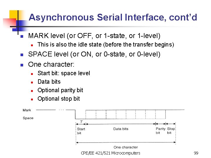
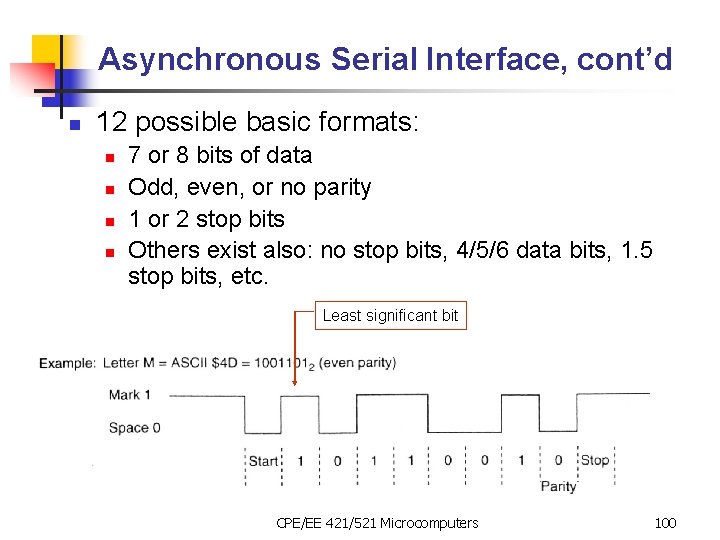
Asynchronous Serial Interface, cont’d n MARK level (or OFF, or 1 -state, or 1 -level) n n n This is also the idle state (before the transfer begins) SPACE level (or ON, or 0 -state, or 0 -level) One character: n n Start bit: space level Data bits Optional parity bit Optional stop bit CPE/EE 421/521 Microcomputers 99

Asynchronous Serial Interface, cont’d n 12 possible basic formats: n n 7 or 8 bits of data Odd, even, or no parity 1 or 2 stop bits Others exist also: no stop bits, 4/5/6 data bits, 1. 5 stop bits, etc. Least significant bit CPE/EE 421/521 Microcomputers 100

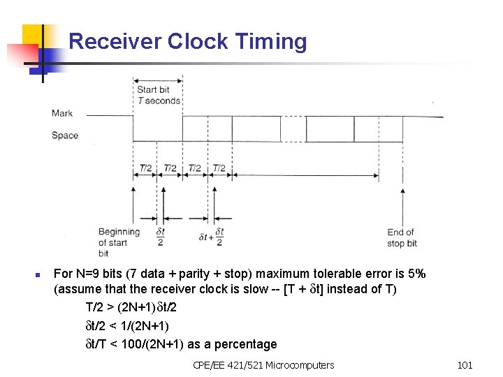
Receiver Clock Timing n For N=9 bits (7 data + parity + stop) maximum tolerable error is 5% (assume that the receiver clock is slow -- [T + dt] instead of T) T/2 > (2 N+1)dt/2 < 1/(2 N+1) dt/T < 100/(2 N+1) as a percentage CPE/EE 421/521 Microcomputers 101

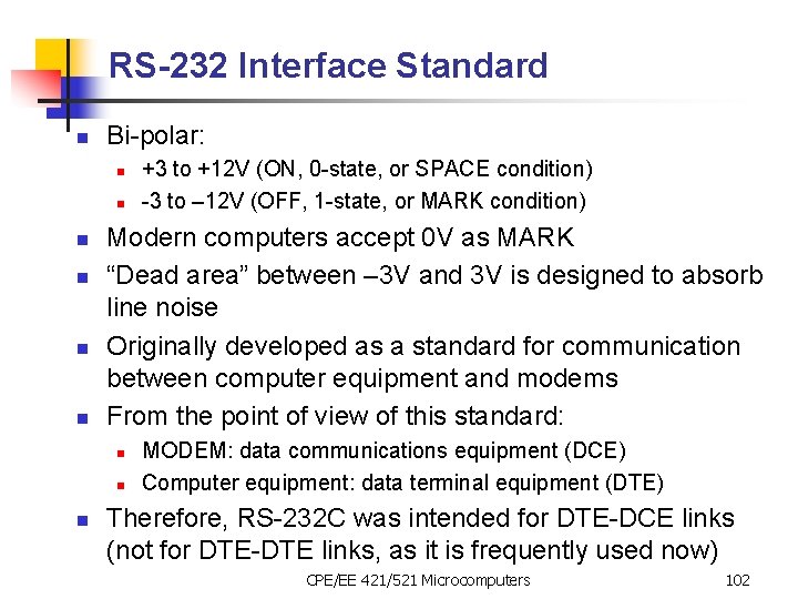
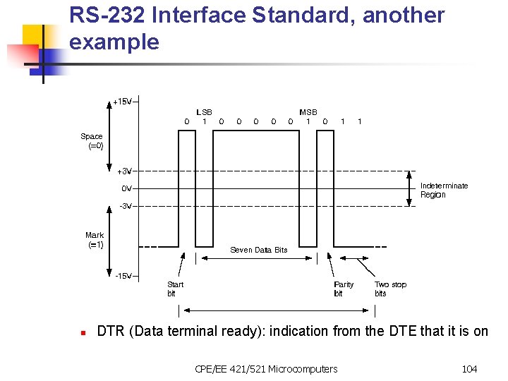
RS-232 Interface Standard n Bi-polar: n n n Modern computers accept 0 V as MARK “Dead area” between – 3 V and 3 V is designed to absorb line noise Originally developed as a standard for communication between computer equipment and modems From the point of view of this standard: n n n +3 to +12 V (ON, 0 -state, or SPACE condition) -3 to – 12 V (OFF, 1 -state, or MARK condition) MODEM: data communications equipment (DCE) Computer equipment: data terminal equipment (DTE) Therefore, RS-232 C was intended for DTE-DCE links (not for DTE-DTE links, as it is frequently used now) CPE/EE 421/521 Microcomputers 102

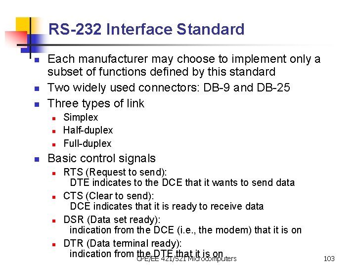
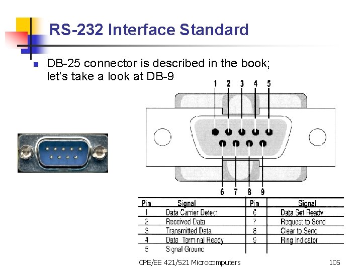
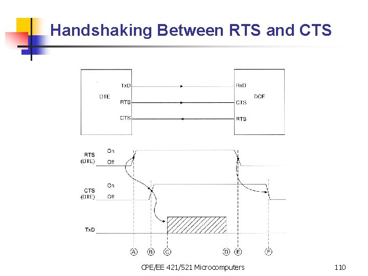
RS-232 Interface Standard n n n Each manufacturer may choose to implement only a subset of functions defined by this standard Two widely used connectors: DB-9 and DB-25 Three types of link n n Simplex Half-duplex Full-duplex Basic control signals n n RTS (Request to send): DTE indicates to the DCE that it wants to send data CTS (Clear to send): DCE indicates that it is ready to receive data DSR (Data set ready): indication from the DCE (i. e. , the modem) that it is on DTR (Data terminal ready): indication from CPE/EE the DTE that it is on 421/521 Microcomputers 103

RS-232 Interface Standard, another example n DTR (Data terminal ready): indication from the DTE that it is on CPE/EE 421/521 Microcomputers 104

RS-232 Interface Standard n DB-25 connector is described in the book; let’s take a look at DB-9 CPE/EE 421/521 Microcomputers 105

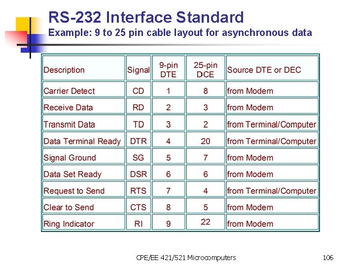
RS-232 Interface Standard Example: 9 to 25 pin cable layout for asynchronous data CPE/EE 421/521 Microcomputers 106

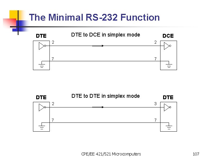
The Minimal RS-232 Function DTE to DCE in simplex mode DTE DCE 2 2 7 7 DTE to DTE in simplex mode DTE 2 3 7 7 CPE/EE 421/521 Microcomputers 107

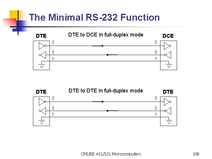
The Minimal RS-232 Function DTE to DCE in full-duplex mode DTE DCE 2 2 3 3 7 7 DTE to DTE in full-duplex mode DTE 2 3 3 2 7 7 CPE/EE 421/521 Microcomputers 108

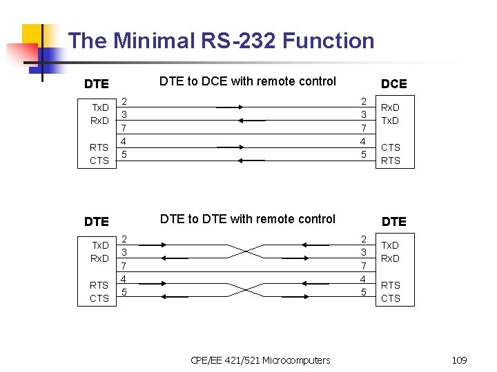
The Minimal RS-232 Function DTE to DCE with remote control DTE Tx. D RTS CTS 2 3 7 4 5 DTE to DTE with remote control DTE Tx. D Rx. D DCE 2 3 7 4 5 CTS RTS DTE 2 3 7 4 5 CPE/EE 421/521 Microcomputers Rx. D Tx. D RTS CTS 109

Handshaking Between RTS and CTS CPE/EE 421/521 Microcomputers 110

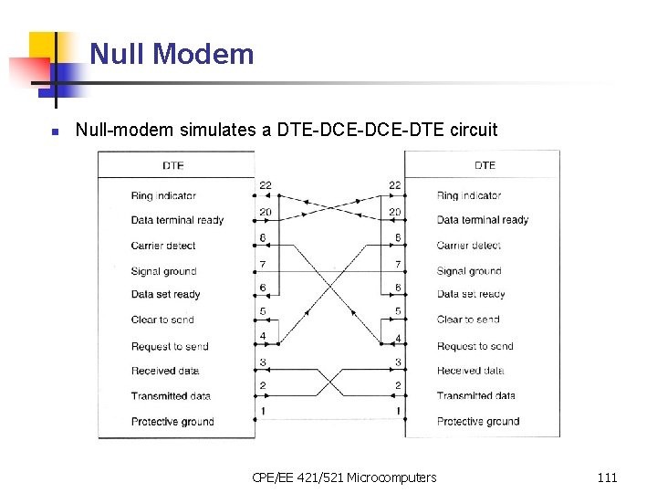
Null Modem n Null-modem simulates a DTE-DCE-DTE circuit CPE/EE 421/521 Microcomputers 111

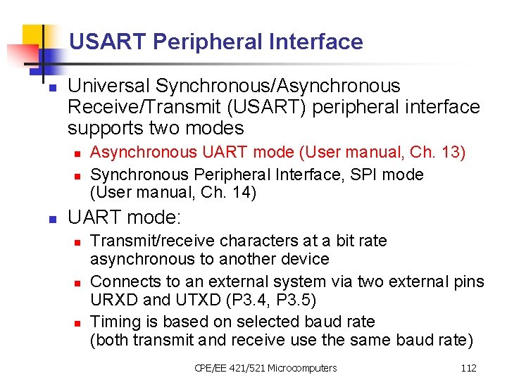
USART Peripheral Interface n Universal Synchronous/Asynchronous Receive/Transmit (USART) peripheral interface supports two modes n n n Asynchronous UART mode (User manual, Ch. 13) Synchronous Peripheral Interface, SPI mode (User manual, Ch. 14) UART mode: n n n Transmit/receive characters at a bit rate asynchronous to another device Connects to an external system via two external pins URXD and UTXD (P 3. 4, P 3. 5) Timing is based on selected baud rate (both transmit and receive use the same baud rate) CPE/EE 421/521 Microcomputers 112

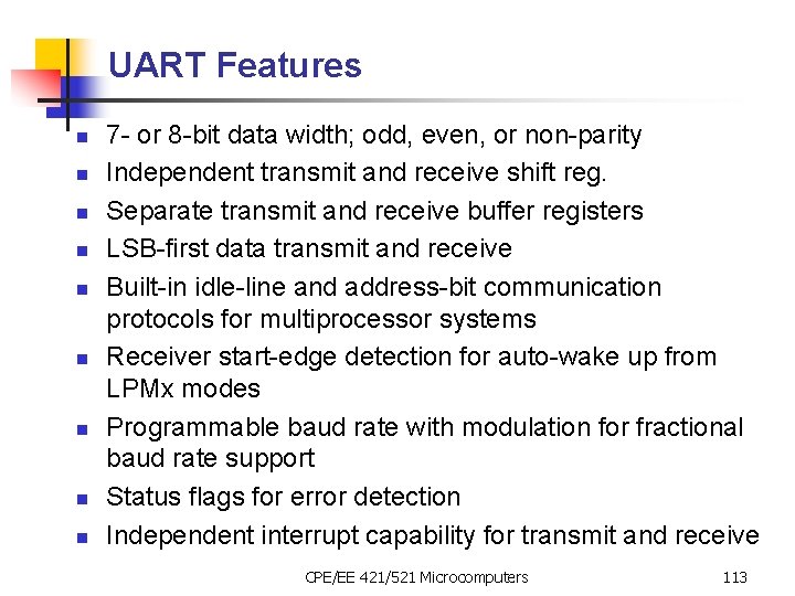
UART Features n n n n n 7 - or 8 -bit data width; odd, even, or non-parity Independent transmit and receive shift reg. Separate transmit and receive buffer registers LSB-first data transmit and receive Built-in idle-line and address-bit communication protocols for multiprocessor systems Receiver start-edge detection for auto-wake up from LPMx modes Programmable baud rate with modulation for fractional baud rate support Status flags for error detection Independent interrupt capability for transmit and receive CPE/EE 421/521 Microcomputers 113

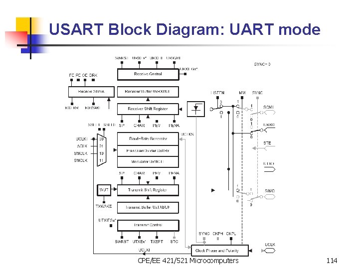
USART Block Diagram: UART mode CPE/EE 421/521 Microcomputers 114

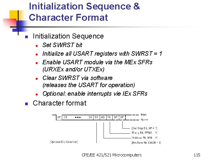
Initialization Sequence & Character Format n Initialization Sequence n n n Set SWRST bit Initialize all USART registers with SWRST = 1 Enable USART module via the MEx SFRs (URXEx and/or UTXEx) Clear SWRST via software (releases the USART for operation) Optional: enable interrupts vie IEx SFRs Character format CPE/EE 421/521 Microcomputers 115

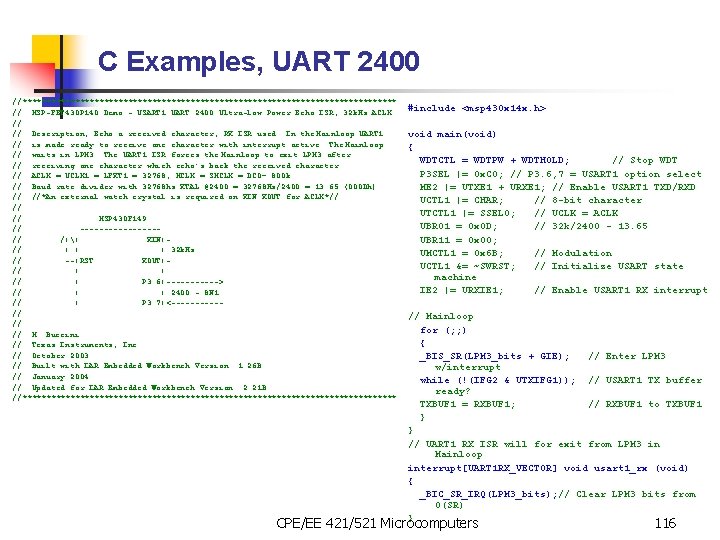
C Examples, UART 2400 //*************************************** // MSP-FET 430 P 140 Demo - USART 1 UART 2400 Ultra-low Power Echo ISR, 32 k. Hz ACLK // // Description; Echo a received character, RX ISR used. In the Mainloop UART 1 // is made ready to receive one character with interrupt active. The Mainloop // waits in LPM 3. The UART 1 ISR forces the Mainloop to exit LPM 3 after // receiving one character which echo's back the received character. // ACLK = UCLK 1 = LFXT 1 = 32768, MCLK = SMCLK = DCO~ 800 k // Baud rate divider with 32768 hz XTAL @2400 = 32768 Hz/2400 = 13. 65 (000 Dh) // //*An external watch crystal is required on XIN XOUT for ACLK*// // // MSP 430 F 149 // --------// /|| XIN|// | | | 32 k. Hz // --|RST XOUT|// | | // | P 3. 6|------> // | | 2400 - 8 N 1 // | P 3. 7|<-----// // // M. Buccini // Texas Instruments, Inc // October 2003 // Built with IAR Embedded Workbench Version: 1. 26 B // January 2004 // Updated for IAR Embedded Workbench Version: 2. 21 B //*************************************** #include <msp 430 x 14 x. h> void main(void) { WDTCTL = WDTPW + WDTHOLD; // Stop WDT P 3 SEL |= 0 x. C 0; // P 3. 6, 7 = USART 1 option select ME 2 |= UTXE 1 + URXE 1; // Enable USART 1 TXD/RXD UCTL 1 |= CHAR; // 8 -bit character UTCTL 1 |= SSEL 0; // UCLK = ACLK UBR 01 = 0 x 0 D; // 32 k/2400 - 13. 65 UBR 11 = 0 x 00; UMCTL 1 = 0 x 6 B; // Modulation UCTL 1 &= ~SWRST; // Initialize USART state machine IE 2 |= URXIE 1; // Enable USART 1 RX interrupt // Mainloop for (; ; ) { _BIS_SR(LPM 3_bits + GIE); // Enter LPM 3 w/interrupt while (!(IFG 2 & UTXIFG 1)); // USART 1 TX buffer ready? TXBUF 1 = RXBUF 1; // RXBUF 1 to TXBUF 1 } } // UART 1 RX ISR will for exit from LPM 3 in Mainloop interrupt[UART 1 RX_VECTOR] void usart 1_rx (void) { _BIC_SR_IRQ(LPM 3_bits); // Clear LPM 3 bits from 0(SR) } CPE/EE 421/521 Microcomputers 116