MSP 430 FR 57 xx Family MSP 430


- Slides: 78

MSP 430 FR 57 xx Family MSP 430 with Embedded FRAM 1

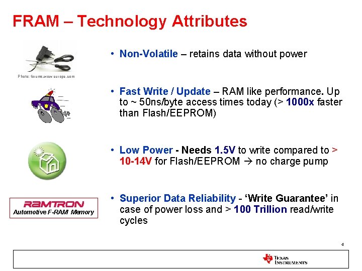
FRAM – Technology Attributes • Non-Volatile – retains data without power Photo: forums. wow-europe. com • Fast Write / Update – RAM like performance. Up to ~ 50 ns/byte access times today (> 1000 x faster than Flash/EEPROM) • Low Power - Needs 1. 5 V to write compared to > 10 -14 V for Flash/EEPROM no charge pump Automotive F-RAM Memory • Superior Data Reliability - ‘Write Guarantee’ in case of power loss and > 100 Trillion read/write cycles 4

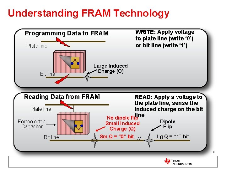
Understanding FRAM Technology Programming Data to FRAM Plate line Bit line Large Induced Charge (Q) Reading Data from FRAM Plate line Ferroelectric Capacitor Bit line WRITE: Apply voltage to plate line (write ‘ 0’) or bit line (write ‘ 1’) READ: Apply a voltage to the plate line, sense the induced charge on the bit line No dipole flip Small Induced Charge (Q) Sm Q = “ 0” bit Dipole Flip Lg Q = “ 1” bit 5

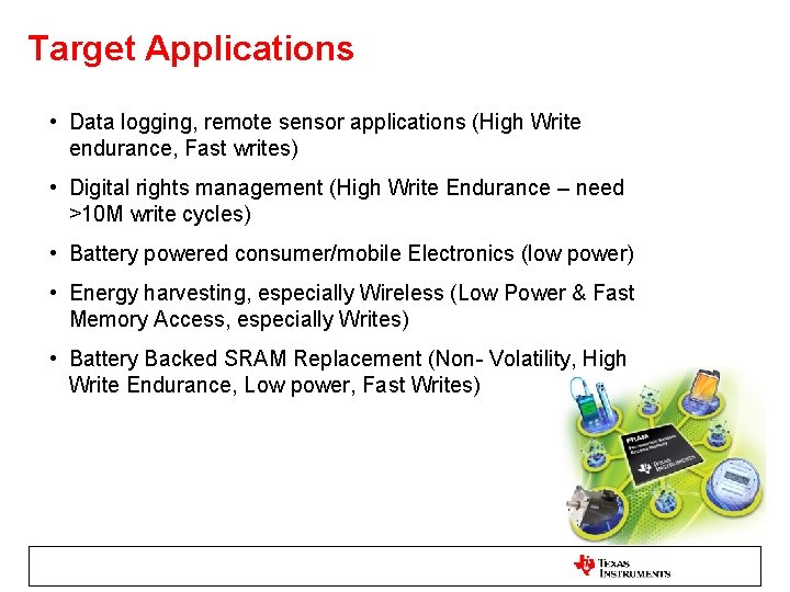
Target Applications • Data logging, remote sensor applications (High Write endurance, Fast writes) • Digital rights management (High Write Endurance – need >10 M write cycles) • Battery powered consumer/mobile Electronics (low power) • Energy harvesting, especially Wireless (Low Power & Fast Memory Access, especially Writes) • Battery Backed SRAM Replacement (Non- Volatility, High Write Endurance, Low power, Fast Writes) 6

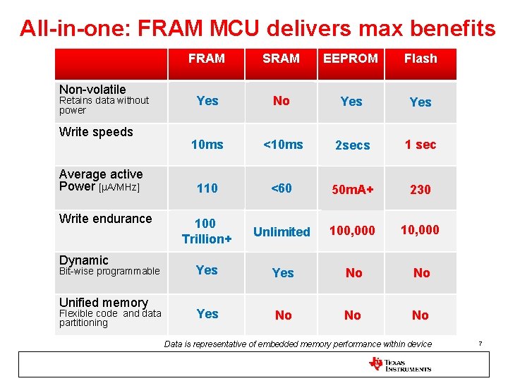
All-in-one: FRAM MCU delivers max benefits FRAM Non-volatile Retains data without power Write speeds Average active Power [µA/MHz] Write endurance Dynamic Bit-wise programmable Unified memory Flexible code and data partitioning SRAM EEPROM Flash Yes No 10 ms <10 ms 2 secs 1 sec 110 <60 50 m. A+ 230 100 Trillion+ Unlimited 100, 000 10, 000 Yes No No No Yes Data is representative of embedded memory performance within device 7

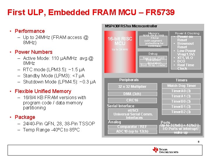
First ULP, Embedded FRAM MCU – FR 5739 • Performance – Up to 24 MHz (FRAM access @ 8 MHz) • Power Numbers – Active Mode: 110 µA/MHz avg. @ 8 MHz – RTC mode (LPM 3. 5): ~1. 5 µA – Standby Mode (LPM 3): <7 µA – Shutdown Mode (LPM 4. 5): ~0. 3 µA • Flexible Unified Memory – 16/8/4 KB FRAM versions with program code / data memory partitioning • Package – 24/40 -Pin QFN, 28, 38 -Pin TSSOP – Temp Range -40ºC to 85ºC MSP 430 FR 57 xx Microcontroller Memory Power & Clocking 16 KB / 8 KB / 4 KB FRAM (with segment protections for code/data) 16 -bit RISC MCU • Power on Reset • Brownout Reset • Low Power Vreg(1. 5 V) • XT 1, VLO • DCO • Real Time Clock Up to 24 MHz Debug Real-time JTAG Embedded Emulation Boot Strap Loader Peripherals 32 x 32 Multiplier DMA (3 ch) CRC 16 Serial Interface e. USCI Universal Serial Comm. Interfaces Analog Comparator / REF ADC 10 (up to 12 ch) Timers Watch Dog Timer. A 0 (3) Timer. A 1 (3) Timer. B 0 (3) Timer. B 1 (3) Timer. B 2 (3) Ports Up to 3 [1 x 8 ] + 1 [1 x 2 ] I/O Ports w/ interrupt/ wake-up 8

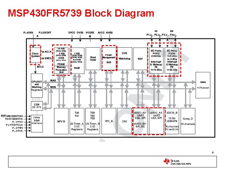
MSP 430 FR 5739 Block Diagram 9

FR 57 xx Architecture & Core Peripherals 10

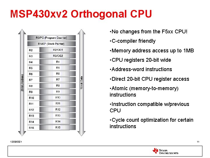
MSP 430 xv 2 Orthogonal CPU • No changes from the F 5 xx CPU! • C-compiler friendly • Memory address access up to 1 MB • CPU registers 20 -bit wide • Address-word instructions • Direct 20 -bit CPU register access • Atomic (memory-to-memory) instructions • Instruction compatible w/previous CPU • Cycle count optimization for certain instructions 12/29/2021 11

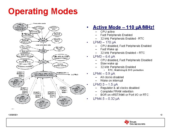
Operating Modes • Active Mode – 110 µA/MHz! – – – • LPM 0 – 170 µA – – – • CPU active Fast Peripherals Enabled 32 k. Hz Peripherals Enabled - RTC CPU disabled, Fast Peripherals Enabled Fast Wake up 32 k. Hz Peripherals Enabled – RTC LPM 3 – 6. 4 µA – – – CPU disabled, Fast Peripherals Disabled Slow wake up 32 k. Hz Peripherals Enabled • • LPM 4 – 5. 9 µA – – • 12/29/2021 All clocks disabled Wake on interrupt LPM 3. 5 – 1. 5 µA – – – • RTC, Watchdog & SVS protection Regulator & all clocks disabled Complete FRAM retention BOR on n. RST/NMI or Port I/O or RTC LPM 4. 5 – 0. 32 µA 12

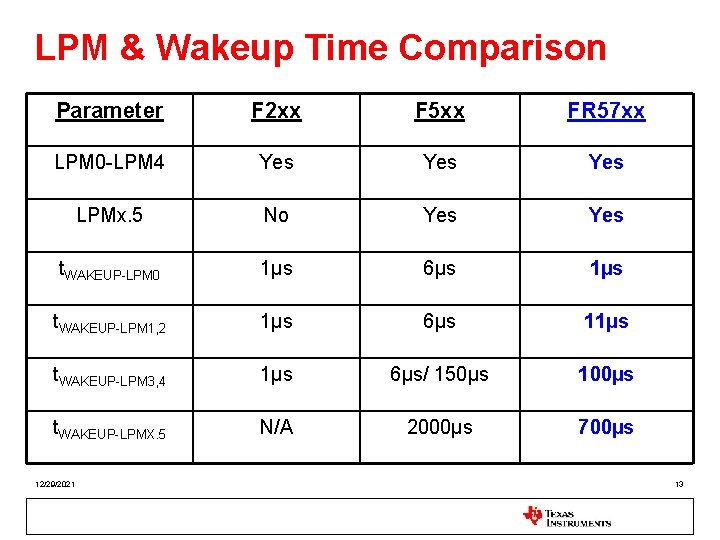
LPM & Wakeup Time Comparison Parameter F 2 xx F 5 xx FR 57 xx LPM 0 -LPM 4 Yes Yes LPMx. 5 No Yes t. WAKEUP-LPM 0 1µs 6µs 1µs t. WAKEUP-LPM 1, 2 1µs 6µs 11µs t. WAKEUP-LPM 3, 4 1µs 6µs/ 150µs 100µs t. WAKEUP-LPMX. 5 N/A 2000µs 700µs 12/29/2021 13

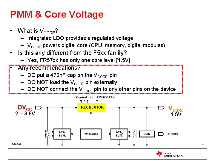
PMM & Core Voltage • What is VCORE? – Integrated LDO provides a regulated voltage – VCORE powers digital core (CPU, memory, digital modules) • Is this any different from the F 5 xx family? – Yes, FR 57 xx has only one core level [1. 5 V] • Any recommendations? – DO put a 470 n. F cap on the VCORE pin – DO NOT load the VCORE pin externally – DO NOT connect the VCORE pin to any other pins on the device DVCC REGULATOR 2 – 3. 6 V 12/29/2021 VCORE 1. 5 V “TI Proprietary Information - Strictly Private” or similar placed here if applicable 14

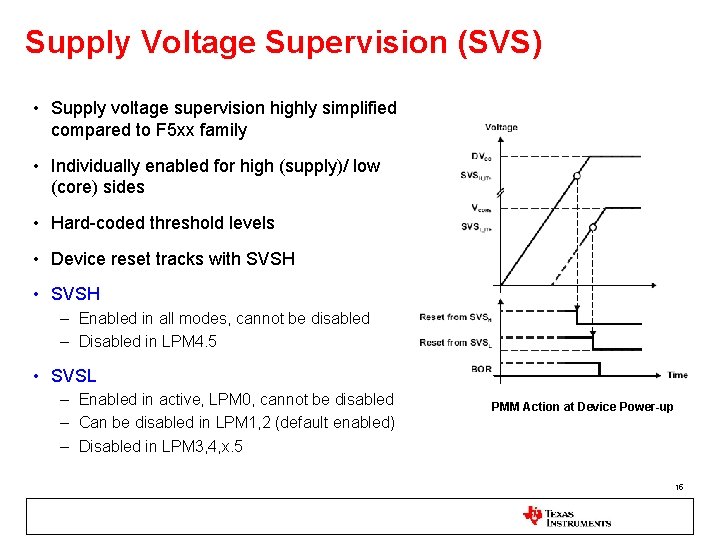
Supply Voltage Supervision (SVS) • Supply voltage supervision highly simplified compared to F 5 xx family • Individually enabled for high (supply)/ low (core) sides • Hard-coded threshold levels • Device reset tracks with SVSH • SVSH – Enabled in all modes, cannot be disabled – Disabled in LPM 4. 5 • SVSL – Enabled in active, LPM 0, cannot be disabled – Can be disabled in LPM 1, 2 (default enabled) – Disabled in LPM 3, 4, x. 5 PMM Action at Device Power-up 15

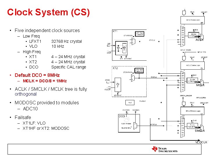
Clock System (CS) • Five independent clock sources – Low Freq • LFXT 1 • VLO – High Freq • XT 1 • XT 2 • DCO 32768 Hz crystal 10 k. Hz ACLK 4 – 24 MHz crystal Specific CAL range • Default DCO = 8 MHz – MCLK = DCO/8 = 1 MHz • ACLK / SMCLK / MCLK tree is fully orthogonal MCLK • MODOSC provided to modules – ADC 10 • Failsafe – XT 1 LF: VLO – XT 1 HF or XT 2: MODOSC SMCLK 16 16 VLOCLK

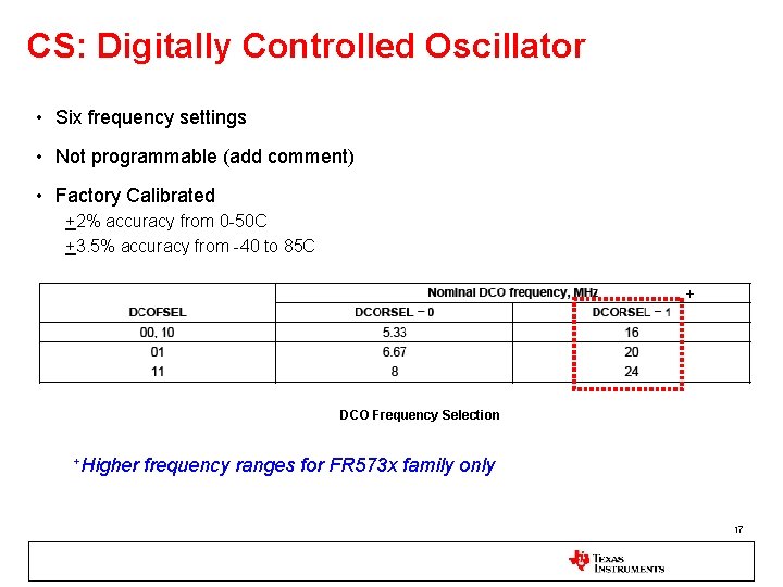
CS: Digitally Controlled Oscillator • Six frequency settings • Not programmable (add comment) • Factory Calibrated +2% accuracy from 0 -50 C +3. 5% accuracy from -40 to 85 C + DCO Frequency Selection +Higher frequency ranges for FR 573 x family only 17

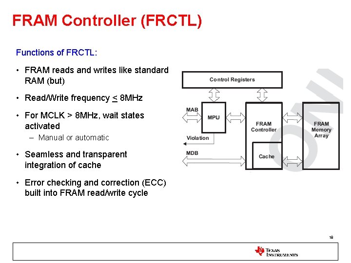
FRAM Controller (FRCTL) Functions of FRCTL: • FRAM reads and writes like standard RAM (but) • Read/Write frequency < 8 MHz • For MCLK > 8 MHz, wait states activated – Manual or automatic • Seamless and transparent integration of cache • Error checking and correction (ECC) built into FRAM read/write cycle 18

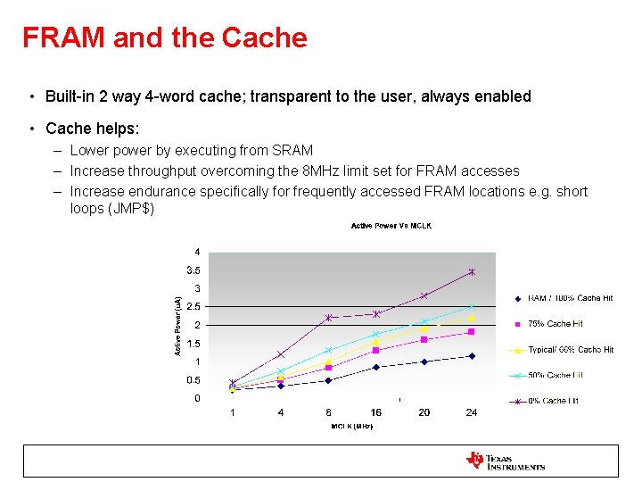
FRAM and the Cache • Built-in 2 way 4 -word cache; transparent to the user, always enabled • Cache helps: – Lower power by executing from SRAM – Increase throughput overcoming the 8 MHz limit set for FRAM accesses – Increase endurance specifically for frequently accessed FRAM locations e. g. short loops (JMP$) 19

So far we’ve covered… • FRAM Technology Attributes • Introduction to the MSP 430 FR 57 xx Family • FR 57 xx CPU, Operating Modes & Wake up times • Core Module Overview – – – PMM SVS CS, DCO FRCTL Impact of Cache in the system Now we are ready for a lab! 20

Lab 1 A Goals: 1) Unboxing the FRAM Experimenter’s Board 2) FRAM EXP feature overview 3) FRAM EXP Graphical User Interface and User Experience 21

Obtaining Lab Software • Software for this lab can be obtained from the MSP 430 FRAM Training Wiki • The link is: http: //processors. wiki. ti. com/index. php/MSP 430_FR 57 xx_3_HR_Lab • Download the zip file – The folder ‘FR-EXP User Experience’ contains the FRAM EXP User Experience Code and the Graphical User Interface used in Lab 1 – The folder ‘Lab. Workspace’ contains the CCS workspace location and the source files for executing the labs 2 & 3 • By default the board is programmed with the User Experience code 22

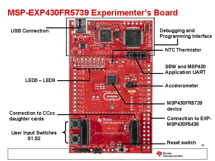
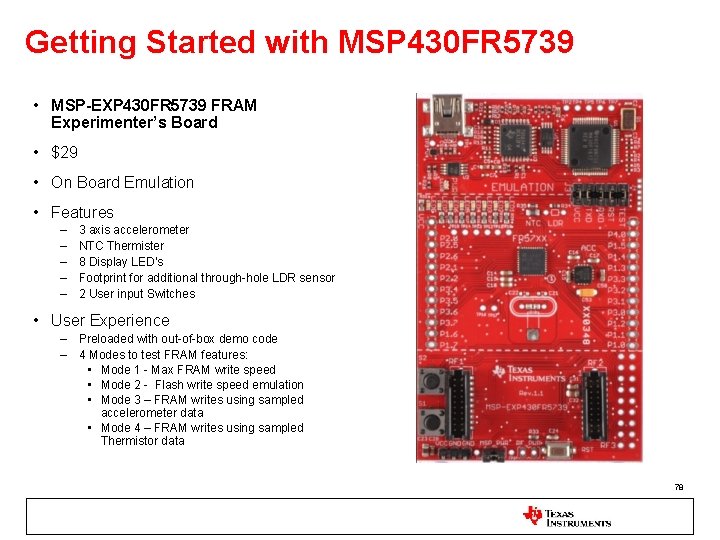
MSP-EXP 430 FR 5739 Experimenter’s Board USB Connection Debugging and Programming Interface NTC Thermistor SBW and MSP 430 Application UART LED 0 – LED 8 Accelerometer Connection to CCxx daughter cards User Input Switches S 1, S 2 MSP 430 FR 5739 device Connection to EXPMSP 430 F 5438 Reset switch 23

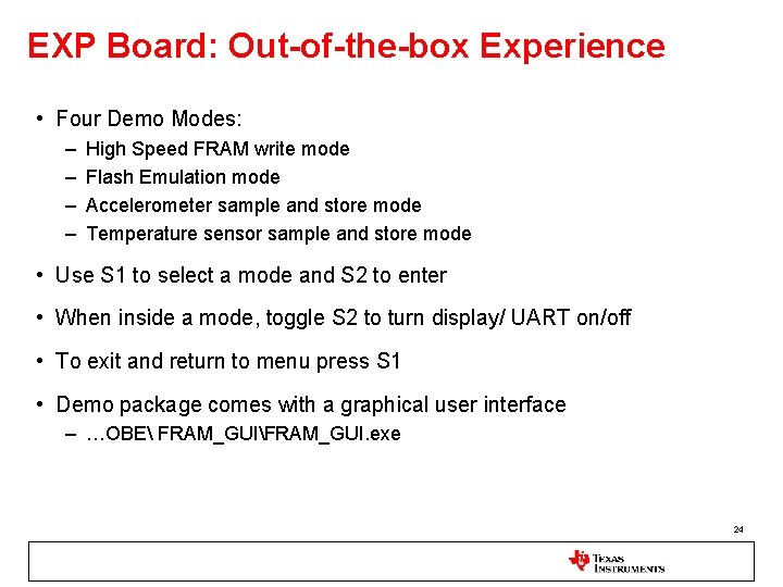
EXP Board: Out-of-the-box Experience • Four Demo Modes: – – High Speed FRAM write mode Flash Emulation mode Accelerometer sample and store mode Temperature sensor sample and store mode • Use S 1 to select a mode and S 2 to enter • When inside a mode, toggle S 2 to turn display/ UART on/off • To exit and return to menu press S 1 • Demo package comes with a graphical user interface – …OBE FRAM_GUIFRAM_GUI. exe 24

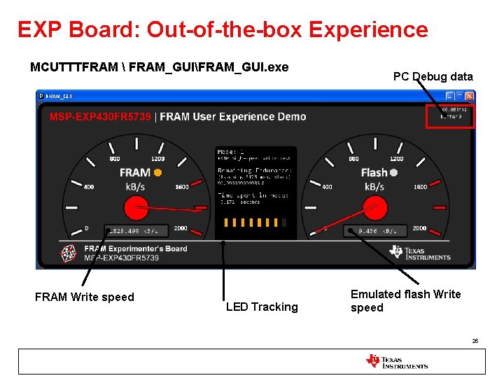
EXP Board: Out-of-the-box Experience MCUTTTFRAM FRAM_GUIFRAM_GUI. exe FRAM Write speed LED Tracking PC Debug data Emulated flash Write speed 25

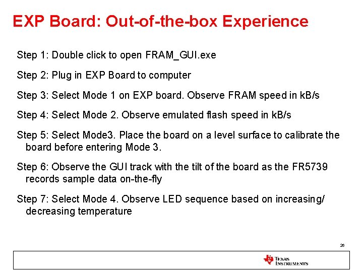
EXP Board: Out-of-the-box Experience Step 1: Double click to open FRAM_GUI. exe Step 2: Plug in EXP Board to computer Step 3: Select Mode 1 on EXP board. Observe FRAM speed in k. B/s Step 4: Select Mode 2. Observe emulated flash speed in k. B/s Step 5: Select Mode 3. Place the board on a level surface to calibrate the board before entering Mode 3. Step 6: Observe the GUI track with the tilt of the board as the FR 5739 records sample data on-the-fly Step 7: Select Mode 4. Observe LED sequence based on increasing/ decreasing temperature 26

Lab 1 B Goals: 1) Setting up a CCS Project 2) Measure active power for different system frequencies 3) Understand the impact of cache on active power 27

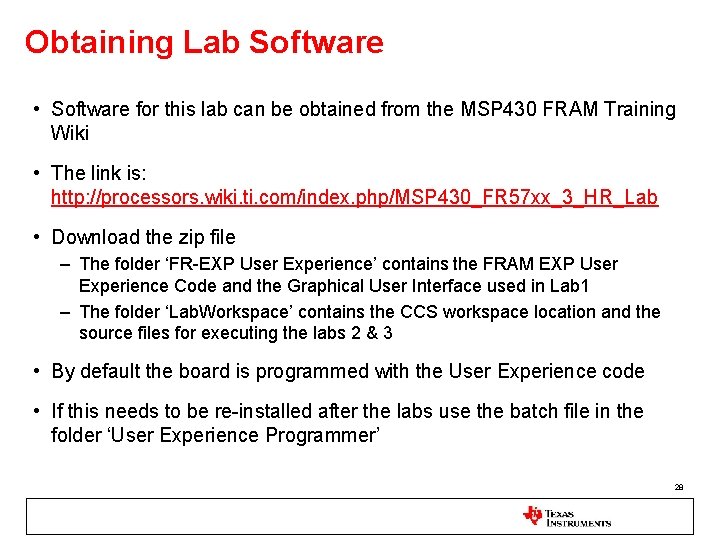
Obtaining Lab Software • Software for this lab can be obtained from the MSP 430 FRAM Training Wiki • The link is: http: //processors. wiki. ti. com/index. php/MSP 430_FR 57 xx_3_HR_Lab • Download the zip file – The folder ‘FR-EXP User Experience’ contains the FRAM EXP User Experience Code and the Graphical User Interface used in Lab 1 – The folder ‘Lab. Workspace’ contains the CCS workspace location and the source files for executing the labs 2 & 3 • By default the board is programmed with the User Experience code • If this needs to be re-installed after the labs use the batch file in the folder ‘User Experience Programmer’ 28

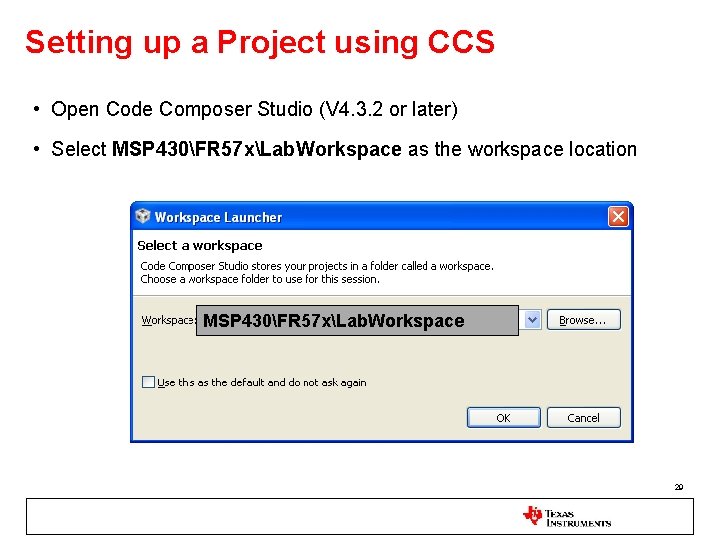
Setting up a Project using CCS • Open Code Composer Studio (V 4. 3. 2 or later) • Select MSP 430FR 57 xLab. Workspace as the workspace location MSP 430FR 57 xLab. Workspace 29

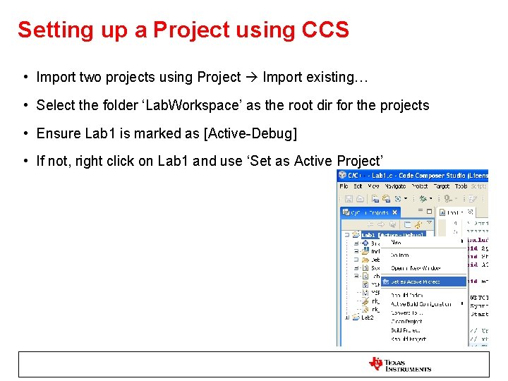
Setting up a Project using CCS • Import two projects using Project Import existing… • Select the folder ‘Lab. Workspace’ as the root dir for the projects • Ensure Lab 1 is marked as [Active-Debug] • If not, right click on Lab 1 and use ‘Set as Active Project’ 30

Using while(1)/ JMP$ to Measure Power Lab Notes: • Lab 1. c is setup to initialize the board, execute the LED startup sequence • Ensure that while(1); loop in main() is included • Build and download active project [Target Debug Active Project] • Execute the code [Target Run] • Terminate Debug Session [Target Terminate All] 31

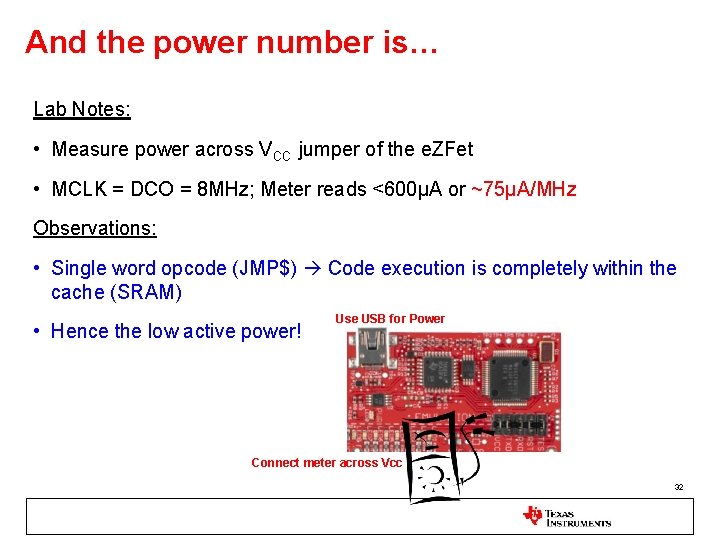
And the power number is… Lab Notes: • Measure power across VCC jumper of the e. ZFet • MCLK = DCO = 8 MHz; Meter reads <600µA or ~75µA/MHz Observations: • Single word opcode (JMP$) Code execution is completely within the cache (SRAM) • Hence the low active power! Use USB for Power Connect meter across Vcc 32

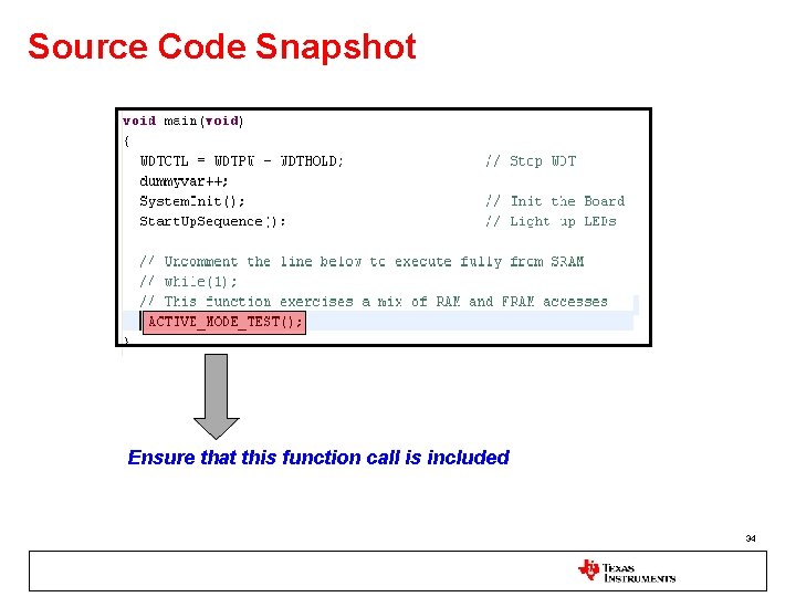
A More Realistic Scenario • Function Active_mode_test() = combination of RAM, FRAM access + different addressing modes • Closer to typical application use-case • Use this function to measure ‘real world’ active power • Comment out the while(1); loop • Include ACTIVE_MODE_TEST() function call • Rebuild Project • Download & execute the code, terminate debug session Note: Remember to reconnect the jumper to program the target or leave the meter ON 33

Source Code Snapshot Ensure that this function call is included 34

And now we measure… Lab Notes • MCLK = DCO = 8 MHz • Meter reads <750µA or <<100µA/MHz Observations: • As # of cache misses increase, active power increases • Cache hit/miss ratio is completely application dependent • Tighter, shorter loops = fewer cache misses 35

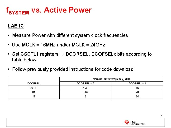
f. SYSTEM vs. Active Power LAB 1 C • Measure Power with different system clock frequencies • Use MCLK = 16 MHz and/or MCLK = 24 MHz • Set CSCTL 1 registers DCORSEL, DCOFSELx bits according to table below • Follow previously provided instructions for code download 36

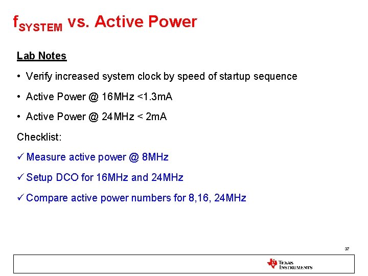
f. SYSTEM vs. Active Power Lab Notes • Verify increased system clock by speed of startup sequence • Active Power @ 16 MHz <1. 3 m. A • Active Power @ 24 MHz < 2 m. A Checklist: Measure active power @ 8 MHz Setup DCO for 16 MHz and 24 MHz Compare active power numbers for 8, 16, 24 MHz 37

FR 57 xx Peripheral Additions & Enhancements 38

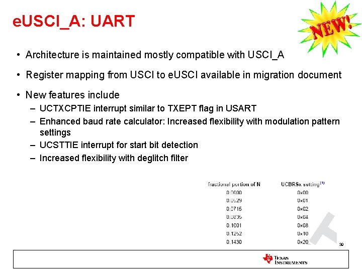
e. USCI_A: UART • Architecture is maintained mostly compatible with USCI_A • Register mapping from USCI to e. USCI available in migration document • New features include – UCTXCPTIE interrupt similar to TXEPT flag in USART – Enhanced baud rate calculator: Increased flexibility with modulation pattern settings – UCSTTIE interrupt for start bit detection – Increased flexibility with deglitch filter 39

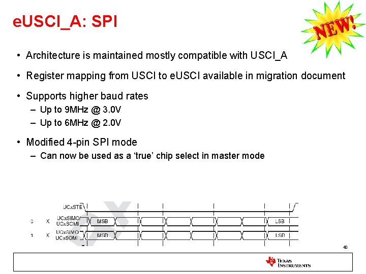
e. USCI_A: SPI • Architecture is maintained mostly compatible with USCI_A • Register mapping from USCI to e. USCI available in migration document • Supports higher baud rates – Up to 9 MHz @ 3. 0 V – Up to 6 MHz @ 2. 0 V • Modified 4 -pin SPI mode – Can now be used as a ‘true’ chip select in master mode 40

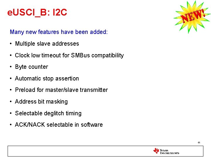
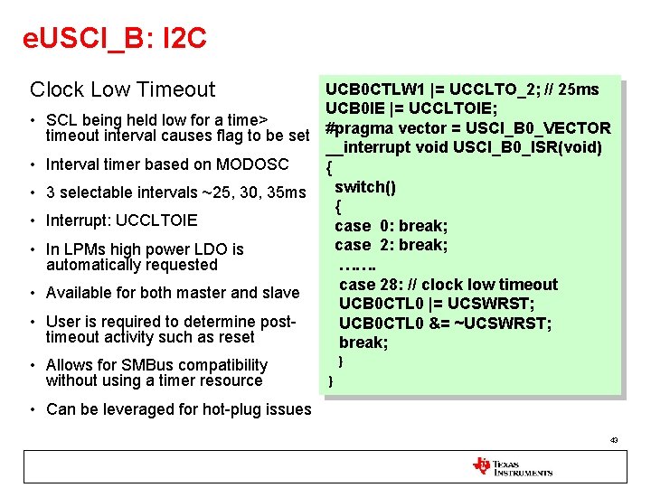
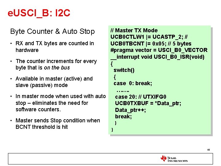
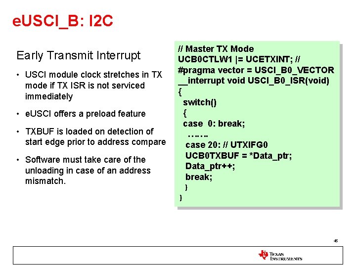
e. USCI_B: I 2 C Many new features have been added: • Multiple slave addresses • Clock low timeout for SMBus compatibility • Byte counter • Automatic stop assertion • Preload for master/slave transmitter • Address bit masking • Selectable deglitch timing • ACK/NACK selectable in software 41

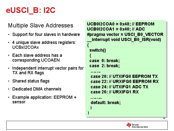
e. USCI_B: I 2 C UCB 0 I 2 COA 0 = 0 x 48; // EEPROM UCB 0 I 2 COA 1 = 0 x 40; // ADC Support for four slaves in hardware #pragma vector = USCI_B 0_VECTOR __interrupt void USCI_B 0_ISR(void) 4 unique slave address registers: { UCBx. I 2 COAx switch() Each slave address has a { corresponding UCOAEN case 0: break; case 2: break; Independent interrupt vector pairs for ……. TX and RX flags case 20: // UTXIFG 0 EEPROM TX Shared status flags case 22: // URXIFG 0 EEPROM RX case 24: // UTXIFG 1 ADC TX Dedicated DMA channels case 26: // URXIFG 1 RX Example application: EEPROM + ……. . sensor default: break; } } Multiple Slave Addresses • • 42

e. USCI_B: I 2 C Clock Low Timeout • • UCB 0 CTLW 1 |= UCCLTO_2; // 25 ms UCB 0 IE |= UCCLTOIE; SCL being held low for a time> timeout interval causes flag to be set #pragma vector = USCI_B 0_VECTOR __interrupt void USCI_B 0_ISR(void) Interval timer based on MODOSC { switch() 3 selectable intervals ~25, 30, 35 ms { Interrupt: UCCLTOIE case 0: break; case 2: break; In LPMs high power LDO is automatically requested ……. case 28: // clock low timeout Available for both master and slave UCB 0 CTL 0 |= UCSWRST; User is required to determine post. UCB 0 CTL 0 &= ~UCSWRST; timeout activity such as reset break; } Allows for SMBus compatibility } without using a timer resource • Can be leveraged for hot-plug issues 43

e. USCI_B: I 2 C // Master TX Mode UCB 0 CTLW 1 |= UCASTP_2; // RX and TX bytes are counted in UCB 0 TBCNT |= 0 x 05; // 5 bytes hardware #pragma vector = USCI_B 0_VECTOR __interrupt void USCI_B 0_ISR(void) The counter increments for every { byte that is on the bus switch() { Available in master (active) and case 0: break; slave (passive) mode ……. In master mode when used with auto case 20: // UTXIFG 0 stop – eliminates the need for UCB 0 TXBUF = *Data_ptr; software counters. Data_ptr++; break; Master sends Stop condition when } BCNT threshold is hit } Byte Counter & Auto Stop • • • 44

e. USCI_B: I 2 C Early Transmit Interrupt • USCI module clock stretches in TX mode if TX ISR is not serviced immediately • e. USCI offers a preload feature • TXBUF is loaded on detection of start edge prior to address compare • Software must take care of the unloading in case of an address mismatch. // Master TX Mode UCB 0 CTLW 1 |= UCETXINT; // #pragma vector = USCI_B 0_VECTOR __interrupt void USCI_B 0_ISR(void) { switch() { case 0: break; ……. case 20: // UTXIFG 0 UCB 0 TXBUF = *Data_ptr; Data_ptr++; break; } } 45

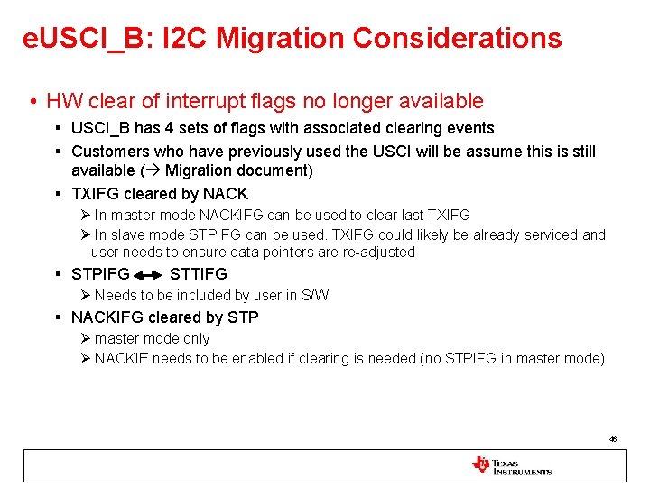
e. USCI_B: I 2 C Migration Considerations • HW clear of interrupt flags no longer available § USCI_B has 4 sets of flags with associated clearing events § Customers who have previously used the USCI will be assume this is still available ( Migration document) § TXIFG cleared by NACK Ø In master mode NACKIFG can be used to clear last TXIFG Ø In slave mode STPIFG can be used. TXIFG could likely be already serviced and user needs to ensure data pointers are re-adjusted § STPIFG STTIFG Ø Needs to be included by user in S/W § NACKIFG cleared by STP Ø master mode only Ø NACKIE needs to be enabled if clearing is needed (no STPIFG in master mode) 46

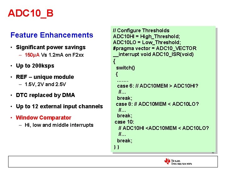
ADC 10_B Feature Enhancements • Significant power savings – 150µA Vs 1. 2 m. A on F 2 xx • Up to 200 ksps • REF – unique module – 1. 5 V, 2 V and 2. 5 V • DTC replaced by DMA • Up to 12 external input channels • Window Comparator – Hi, low and middle interrupts // Configure Thresholds ADC 10 HI = High_Threshold; ADC 10 LO = Low_Threshold; #pragma vector = ADC 10_VECTOR __interrupt void ADC 10_ISR(void) { switch() { ……. case 6: // ADC 10 MEM > ADC 10 HI? //… break; case 8: // ADC 10 MEM < ADC 10 LO? //… break; case 10: // ADC 10 HI <ADC 10 MEM < ADC 10 LO? //… break; }} 47

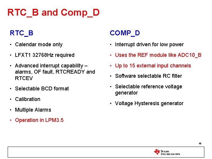
RTC_B and Comp_D RTC_B COMP_D • Calendar mode only • Interrupt driven for low power • LFXT 1 32768 Hz required • Uses the REF module like ADC 10_B • Advanced interrupt capability – alarms, OF fault, RTCREADY and RTCEV • Up to 15 external input channels • Selectable BCD format • Selectable reference voltage generator • Calibration • Software selectable RC filter • Voltage Hysteresis generator • Multiple Alarms • Operation in LPM 3. 5 48

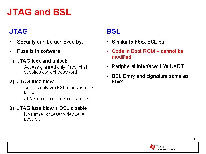
JTAG and BSL JTAG BSL • Security can be achieved by: • Similar to F 5 xx BSL but • Fuse is in software • Code in Boot ROM – cannot be modified 1) JTAG lock and unlock - Access granted only if tool chain supplies correct password 2) JTAG fuse blow - • Peripheral Interface: HW UART • BSL Entry and signature same as F 5 xx Access only via BSL if password is know JTAG can be re-enabled via BSL 3) JTAG fuse blow + BSL disable - No further access to device is possible 49

Using FRAM on the FR 57 xx 50

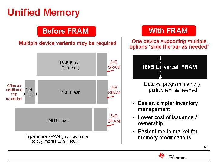
Unified Memory With FRAM Before FRAM Multiple device variants may be required Often an additional 1 k. B chip EEPROM is needed 16 k. B Flash (Program) 2 k. B SRAM 14 k. B Flash 2 k. B SRAM 24 k. B Flash To get more SRAM you may have to buy more FLASH ROM 5 k. B SRAM One device supporting multiple options “slide the bar as needed” 16 k. B Universal FRAM Data vs. program memory partitioned as needed • Easier, simpler inventory management • Lower cost of issuance / ownership • Faster time to market for memory modifications 51

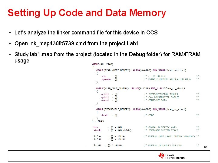
Setting Up Code and Data Memory • Let’s analyze the linker command file for this device in CCS • Open lnk_msp 430 fr 5739. cmd from the project Lab 1 • Study lab 1. map from the project (located in the Debug folder) for RAM/FRAM usage 52

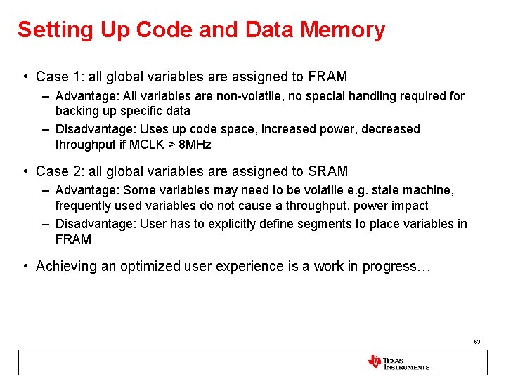
Setting Up Code and Data Memory • Case 1: all global variables are assigned to FRAM – Advantage: All variables are non-volatile, no special handling required for backing up specific data – Disadvantage: Uses up code space, increased power, decreased throughput if MCLK > 8 MHz • Case 2: all global variables are assigned to SRAM – Advantage: Some variables may need to be volatile e. g. state machine, frequently used variables do not cause a throughput, power impact – Disadvantage: User has to explicitly define segments to place variables in FRAM • Achieving an optimized user experience is a work in progress… 53

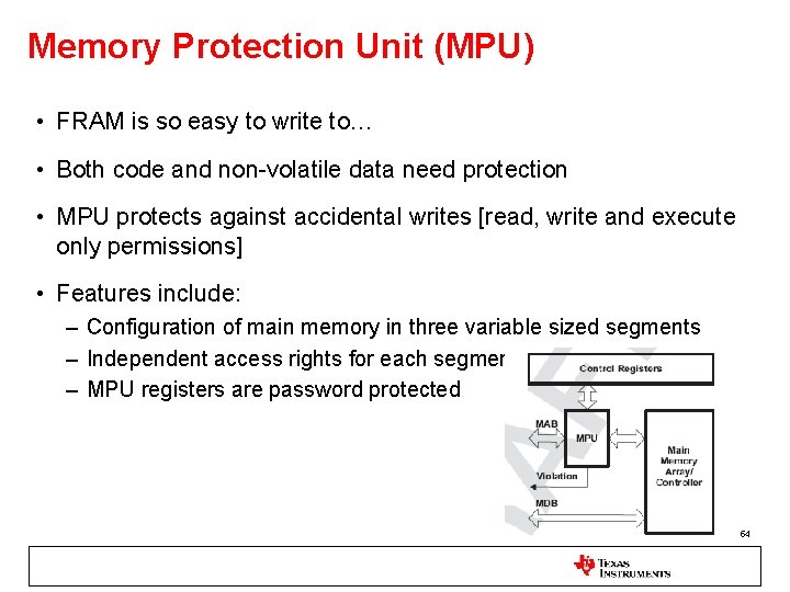
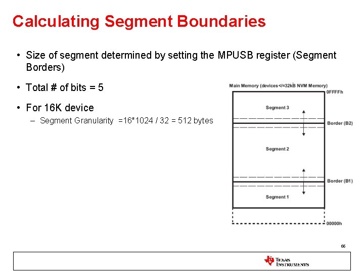
Memory Protection Unit (MPU) • FRAM is so easy to write to… • Both code and non-volatile data need protection • MPU protects against accidental writes [read, write and execute only permissions] • Features include: – Configuration of main memory in three variable sized segments – Independent access rights for each segment – MPU registers are password protected 54

Calculating Segment Boundaries • Size of segment determined by setting the MPUSB register (Segment Borders) • Total # of bits = 5 • For 16 K device – Segment Granularity =16*1024 / 32 = 512 bytes 55

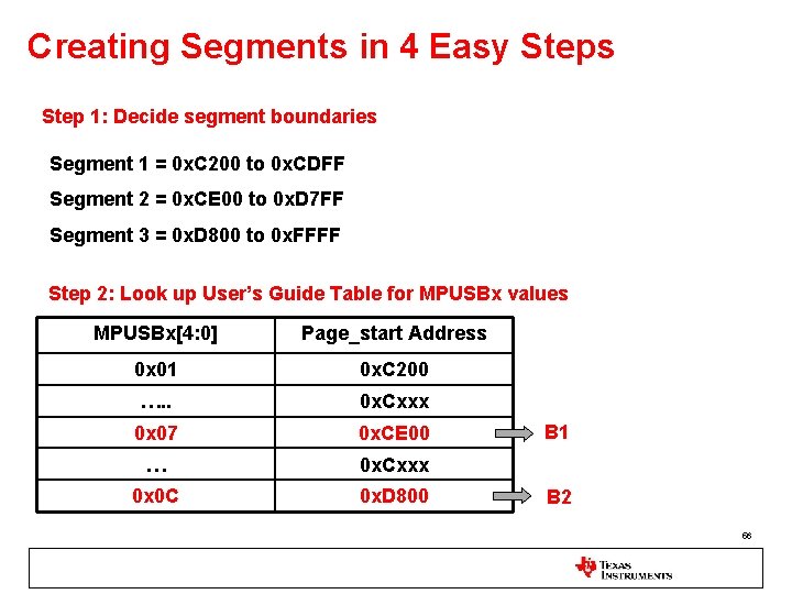
Creating Segments in 4 Easy Steps Step 1: Decide segment boundaries Segment 1 = 0 x. C 200 to 0 x. CDFF Segment 2 = 0 x. CE 00 to 0 x. D 7 FF Segment 3 = 0 x. D 800 to 0 x. FFFF Step 2: Look up User’s Guide Table for MPUSBx values MPUSBx[4: 0] Page_start Address 0 x 01 0 x. C 200 …. . 0 x. Cxxx 0 x 07 0 x. CE 00 … 0 x. Cxxx 0 x 0 C 0 x. D 800 B 1 B 2 56

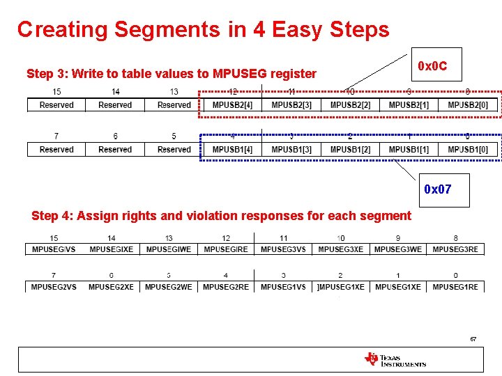
Creating Segments in 4 Easy Steps Step 3: Write to table values to MPUSEG register 0 x 0 C 0 x 07 Step 4: Assign rights and violation responses for each segment 57

Lab 2 Goals: 1) Study MPU registers 2) Assign Segment Boundaries using the User’s Guide Table 3)Assign segment rights and violation response as indicated 58

Obtaining Lab Software • Software for this lab can be obtained from the MSP 430 FRAM Training Wiki • The link is: http: //processors. wiki. ti. com/index. php/MSP 430_FR 57 xx_3_HR_Lab • Download the zip file – The folder ‘FR-EXP User Experience’ contains the FRAM EXP User Experience Code and the Graphical User Interface used in Lab 1 – The folder ‘Lab. Workspace’ contains the CCS workspace location and the source files for executing the labs 2 & 3 • By default the board is programmed with the User Experience code • If this needs to be re-installed after the labs use the batch file in the folder ‘User Experience Programmer’ 59

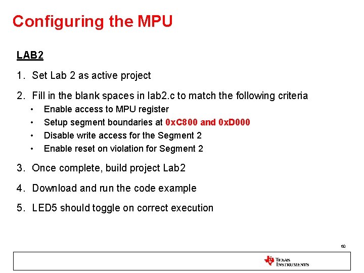
Configuring the MPU LAB 2 1. Set Lab 2 as active project 2. Fill in the blank spaces in lab 2. c to match the following criteria • • Enable access to MPU register Setup segment boundaries at 0 x. C 800 and 0 x. D 000 Disable write access for the Segment 2 Enable reset on violation for Segment 2 3. Once complete, build project Lab 2 4. Download and run the code example 5. LED 5 should toggle on correct execution 60

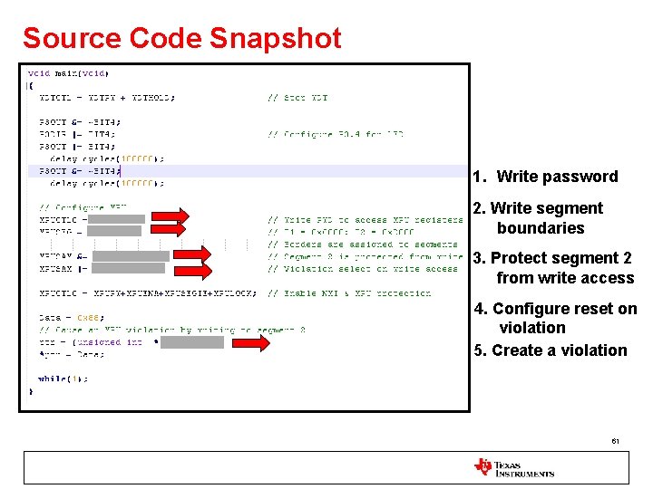
Source Code Snapshot 1. Write password 2. Write segment boundaries 3. Protect segment 2 from write access 4. Configure reset on violation 5. Create a violation 61

Configuring the MPU LAB 2 Observations: • MPU is essential to protect code vs. data memory • MPU can be programmed to reset the device in case of an access violation Checklist: Learn about the MPU registers Configure Segment Boundaries Create individual access rights for each segment Assign violation response per segment 62

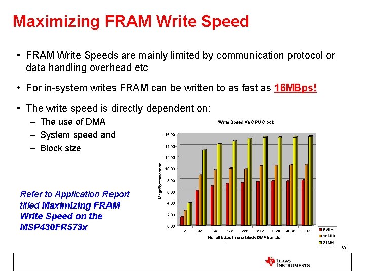
Maximizing FRAM Write Speed • FRAM Write Speeds are mainly limited by communication protocol or data handling overhead etc • For in-system writes FRAM can be written to as fast as 16 MBps! • The write speed is directly dependent on: – The use of DMA – System speed and – Block size Refer to Application Report titled Maximizing FRAM Write Speed on the MSP 430 FR 573 x 63

Differentiating with the FR 57 xx 64

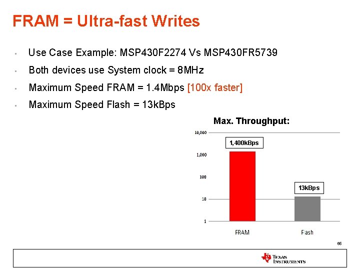
FRAM = Ultra-fast Writes • Use Case Example: MSP 430 F 2274 Vs MSP 430 FR 5739 • Both devices use System clock = 8 MHz • Maximum Speed FRAM = 1. 4 Mbps [100 x faster] • Maximum Speed Flash = 13 k. Bps Max. Throughput: 1, 400 k. Bps 13 k. Bps 65

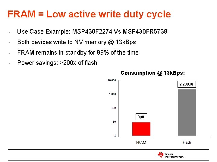
FRAM = Low active write duty cycle • Use Case Example: MSP 430 F 2274 Vs MSP 430 FR 5739 • Both devices write to NV memory @ 13 k. Bps • FRAM remains in standby for 99% of the time • Power savings: >200 x of flash Consumption @ 13 k. Bps: 2, 200μA 9μA 66

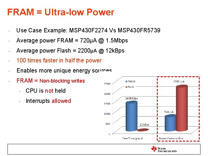
FRAM = Ultra-low Power • Use Case Example: MSP 430 F 2274 Vs MSP 430 FR 5739 • Average power FRAM = 720µA @ 1. 5 Mbps • Average power Flash = 2200µA @ 12 k. Bps • 100 times faster in half the power • Enables more unique energy sources • FRAM = Non-blocking writes • CPU is not held • Interrupts allowed 67

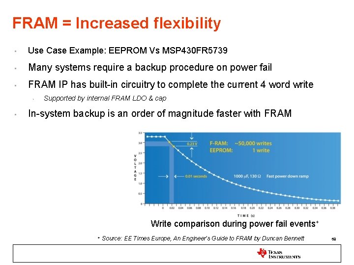
FRAM = Increased flexibility • Use Case Example: EEPROM Vs MSP 430 FR 5739 • Many systems require a backup procedure on power fail • FRAM IP has built-in circuitry to complete the current 4 word write • • Supported by internal FRAM LDO & cap In-system backup is an order of magnitude faster with FRAM Write comparison during power fail events+ + Source: EE Times Europe, An Engineer’s Guide to FRAM by Duncan Bennett 68

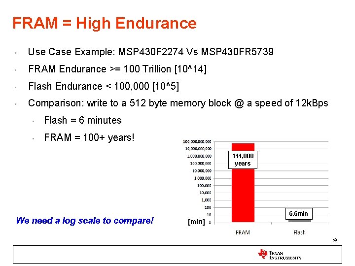
FRAM = High Endurance • Use Case Example: MSP 430 F 2274 Vs MSP 430 FR 5739 • FRAM Endurance >= 100 Trillion [10^14] • Flash Endurance < 100, 000 [10^5] • Comparison: write to a 512 byte memory block @ a speed of 12 k. Bps • Flash = 6 minutes • FRAM = 100+ years! 114, 000 years We need a log scale to compare! 6. 6 min [min] 69

FRAM and Reliability 70

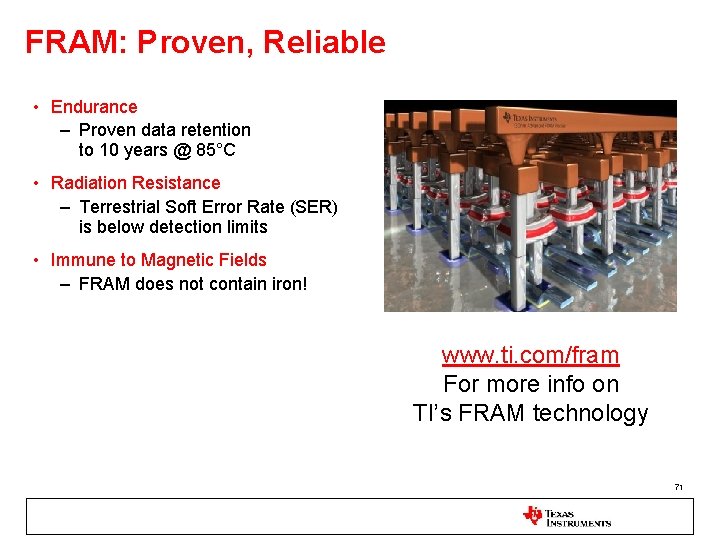
FRAM: Proven, Reliable • Endurance – Proven data retention to 10 years @ 85°C • Radiation Resistance – Terrestrial Soft Error Rate (SER) is below detection limits • Immune to Magnetic Fields – FRAM does not contain iron! www. ti. com/fram For more info on TI’s FRAM technology 71

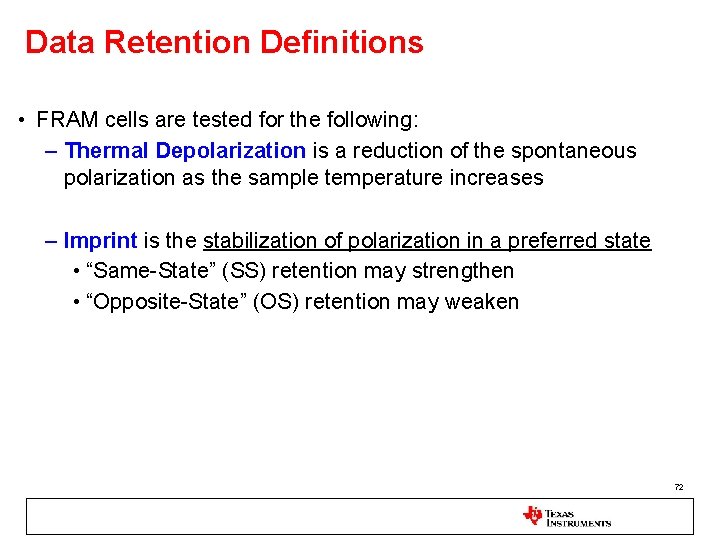
Data Retention Definitions • FRAM cells are tested for the following: – Thermal Depolarization is a reduction of the spontaneous polarization as the sample temperature increases – Imprint is the stabilization of polarization in a preferred state • “Same-State” (SS) retention may strengthen • “Opposite-State” (OS) retention may weaken 72

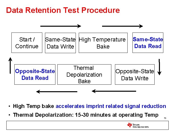
Data Retention Test Procedure Start / Continue Same-State High Temperature Bake Data Write Opposite-State Data Read Thermal Depolarization Bake Same-State Data Read Opposite-State Data Write • High Temp bake accelerates imprint related signal reduction • Thermal Depolarization: 15 -30 minutes at operating Temp 73

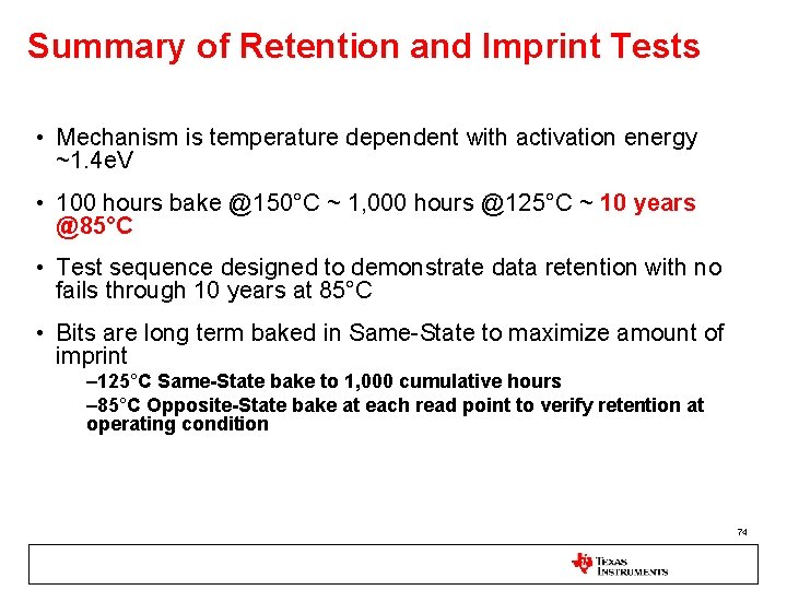
Summary of Retention and Imprint Tests • Mechanism is temperature dependent with activation energy ~1. 4 e. V • 100 hours bake @150°C ~ 1, 000 hours @125°C ~ 10 years @85°C • Test sequence designed to demonstrate data retention with no fails through 10 years at 85°C • Bits are long term baked in Same-State to maximize amount of imprint – 125°C Same-State bake to 1, 000 cumulative hours – 85°C Opposite-State bake at each read point to verify retention at operating condition 74

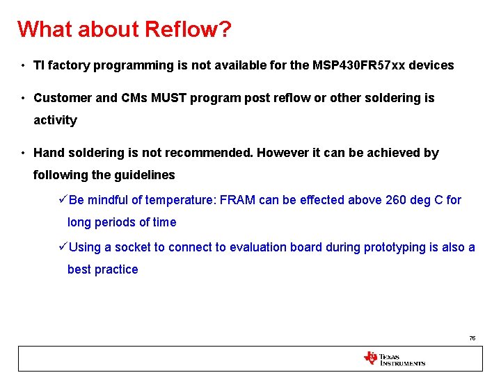
What about Reflow? • TI factory programming is not available for the MSP 430 FR 57 xx devices • Customer and CMs MUST program post reflow or other soldering is activity • Hand soldering is not recommended. However it can be achieved by following the guidelines Be mindful of temperature: FRAM can be effected above 260 deg C for long periods of time Using a socket to connect to evaluation board during prototyping is also a best practice 75

Tools & Resources 76

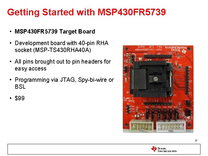
Getting Started with MSP 430 FR 5739 • MSP 430 FR 5739 Target Board • Development board with 40 -pin RHA socket (MSP-TS 430 RHA 40 A) • All pins brought out to pin headers for easy access • Programming via JTAG, Spy-bi-wire or BSL • $99 77

Getting Started with MSP 430 FR 5739 • MSP-EXP 430 FR 5739 FRAM Experimenter’s Board • $29 • On Board Emulation • Features – – – 3 axis accelerometer NTC Thermister 8 Display LED’s Footprint for additional through-hole LDR sensor 2 User input Switches • User Experience – Preloaded with out-of-box demo code – 4 Modes to test FRAM features: • Mode 1 - Max FRAM write speed • Mode 2 - Flash write speed emulation • Mode 3 – FRAM writes using sampled accelerometer data • Mode 4 – FRAM writes using sampled Thermistor data 78

Getting Started with MSP 430 FR 5739 • www. ti. com/fram • Product Page from www. msp 430. com • Upcoming Collateral: – – – – Maximizing FRAM Write Speed FR 57 xx Migration Guide FR-EXP Tool User’s Guide FRAM Reliability Application Report Code Examples Embedded Developers Guide to FRAM for Dummies by V. C. Kumar 80

To Summarize FRAM is real! The world’s first ultra-low power catalog FRAM microcontroller is here. • Top 3 FRAM sellers are: – Ultra-fast writes – Ultra-low power – Super high endurance • FR 5739: Great general purpose MCU enhanced by FRAM • FR 5739: Targets niche applications where only FRAM makes sense • Check out our Demos! 81