1 MODULE4 FlipFlops Registers and Counters 2 WARNING



- Slides: 111

1 MODULE-4 Flip-Flops, Registers and Counters

2 WARNING • KEEP YOUR MOBILE PHONE SWITCH OFF IN CLASS.

3 Books Referred • Text Book: • Donald P Leach, Albert Paul Malvino & Goutam Saha: Digital Principles and Applications, 7 th Edition, Tata Mc. Graw Hill, 2015 • Reference Books: • Anil K. Maini: Digital Electronics Principles, Devices and Applications, 2007, John Wiley & Sons, Ltd. • Thomas L. Floyd: Digital Fundamentals, 9 th Edition. , Pearson International Edition. • M. Morris Mano, Michael D. Ciletti : Digital Design With an Introduction to the Verilog HDL, 5 th Edition, Pearson Education, Inc

4 Objective • Flip-Flops • • • Discuss some of the timing problems related to flip-flops Draw a diagram of a JK master-slave flip-flop and describe its operation State the cause of contact bounce and describe a solution for this problem Describe characteristic equations of Flip-Flops and analysis techniques of sequential circuit. Describe excitation table of Flip-Flops. • Register • Understand serial in-serial out shift registers and be familiar with the basic features of the 74 LS 91 • • register Understand serial in-parallel out shift registers and be familiar with the basic features of the 74164 register Understand parallel in-serial out shift registers and be familiar with the basic features of the 74166 register Understand parallel in-parallel out shift registers and be familiar with the basic features of the 74174 and 7495 A registers Understand working of Universal shift register with the basic features of the 74194 register. State various uses of shift registers • • Describe the basic construction and operation of an asynchronous counter Determine the logic circuit needed to decode a given state from the output of a given counter Describe the synchronous counter and its advantages See how the modulus of a counter can be reduced by skipping one or more of its natural counts • • Counter

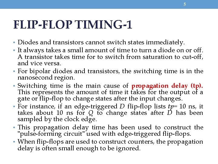
5 FLIP-FLOP TIMING-1 • Diodes and transistors cannot switch states immediately. • It always takes a small amount of time to turn a diode on or off. • • • A transistor takes time for to switch from saturation to cut-off, and vice versa. For bipolar diodes and transistors, the switching time is in the nanosecond region. Switching time is the main cause of propagation delay (tp). This represents the amount of time it takes for the output of a gate or flip-flop to change states after the input changes. For instance, if an edge-triggered D flip-flop lists tp= 10 ns, it takes about 10 ns for Q to change states after D has been sampled by the clock edge. This propagation delay time has been used to construct the "pulse-forming circuit" used with edge-triggered flip-flops. When flip-flops are used to construct counters, the propagation delay is often small enough to be ignored.

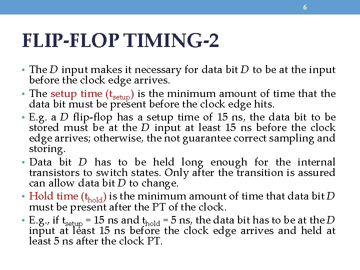
6 FLIP-FLOP TIMING-2 • The D input makes it necessary for data bit D to be at the input • • • before the clock edge arrives. The setup time (tsetup) is the minimum amount of time that the data bit must be present before the clock edge hits. E. g. a D flip-flop has a setup time of 15 ns, the data bit to be stored must be at the D input at least 15 ns before the clock edge arrives; otherwise, the not guarantee correct sampling and storing. Data bit D has to be held long enough for the internal transistors to switch states. Only after the transition is assured can allow data bit D to change. Hold time (thold) is the minimum amount of time that data bit D must be present after the PT of the clock. E. g. , if tsetup = 15 ns and thold = 5 ns, the data bit has to be at the D input at least 15 ns before the clock edge arrives and held at least 5 ns after the clock PT.

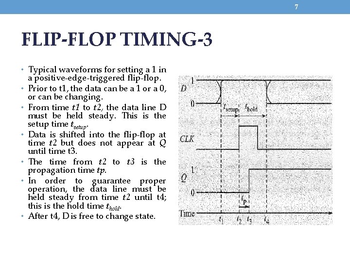
7 FLIP-FLOP TIMING-3 • Typical waveforms for setting a 1 in • • • a positive-edge-triggered flip-flop. Prior to t 1, the data can be a 1 or a 0, or can be changing. From time t 1 to t 2, the data line D must be held steady. This is the setup time tsetup. Data is shifted into the flip-flop at time t 2 but does not appear at Q until time t 3. The time from t 2 to t 3 is the propagation time tp. In order to guarantee properation, the data line must be held steady from time t 2 until t 4; this is the hold time thold. After t 4, D is free to change state.

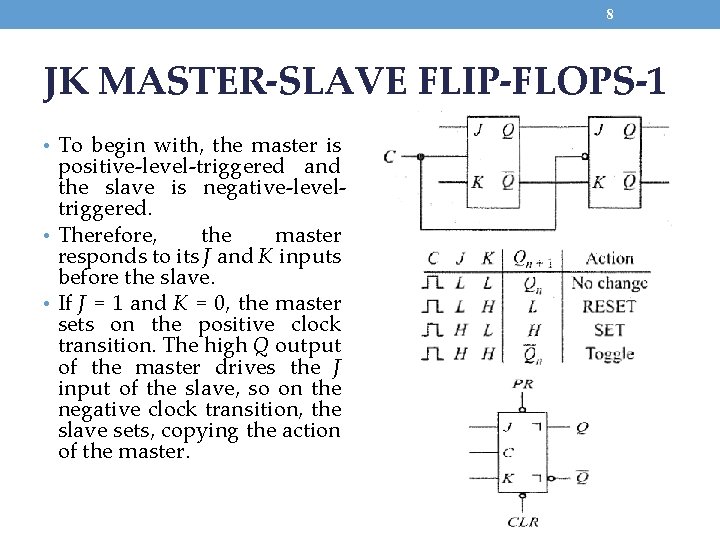
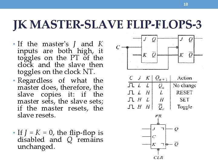
8 JK MASTER-SLAVE FLIP-FLOPS-1 • To begin with, the master is positive-level-triggered and the slave is negative-leveltriggered. • Therefore, the master responds to its J and K inputs before the slave. • If J = 1 and K = 0, the master sets on the positive clock transition. The high Q output of the master drives the J input of the slave, so on the negative clock transition, the slave sets, copying the action of the master.

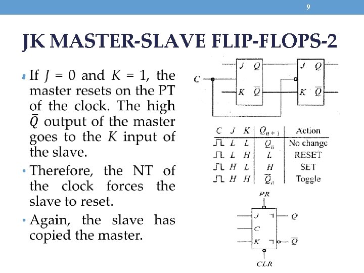
9 JK MASTER-SLAVE FLIP-FLOPS-2 •

10 JK MASTER-SLAVE FLIP-FLOPS-3 • If the master's J and K inputs are both high, it toggles on the PT of the clock and the slave then toggles on the clock NT. • Regardless of what the master does, therefore, the slave copies it: if the master sets, the slave sets; if the master resets, the slave resets. • If J = K = 0, the flip-flop is disabled and Q remains unchanged.

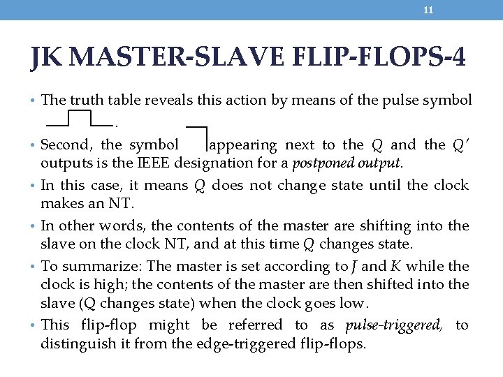
11 JK MASTER-SLAVE FLIP-FLOPS-4 • The truth table reveals this action by means of the pulse symbol • • • . Second, the symbol appearing next to the Q and the Q’ outputs is the IEEE designation for a postponed output. In this case, it means Q does not change state until the clock makes an NT. In other words, the contents of the master are shifting into the slave on the clock NT, and at this time Q changes state. To summarize: The master is set according to J and K while the clock is high; the contents of the master are then shifted into the slave (Q changes state) when the clock goes low. This flip-flop might be referred to as pulse-triggered, to distinguish it from the edge-triggered flip-flops.

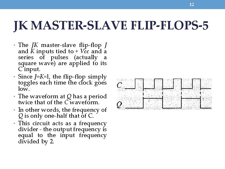
12 JK MASTER-SLAVE FLIP-FLOPS-5 • The JK master-slave flip-flop J • • and K inputs tied to + Vcc and a series of pulses (actually a square wave) are applied to its C input. Since J=K=l, the flip-flop simply toggles each time the clock goes low. The waveform at Q has a period twice that of the C waveform. In other words, the frequency of Q is only one-half that of C. This circuit acts as a frequency divider - the output frequency is equal to the input frequency divided by 2.

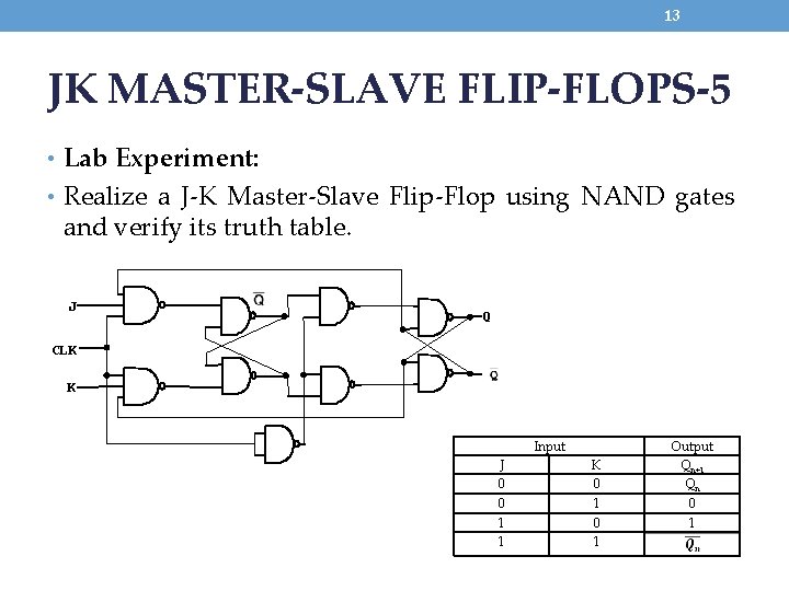
13 JK MASTER-SLAVE FLIP-FLOPS-5 • Lab Experiment: • Realize a J-K Master-Slave Flip-Flop using NAND gates and verify its truth table. J Q CLK K Input J 0 0 K 0 1 1 1 0 1 Output Qn+1 Qn 0 1

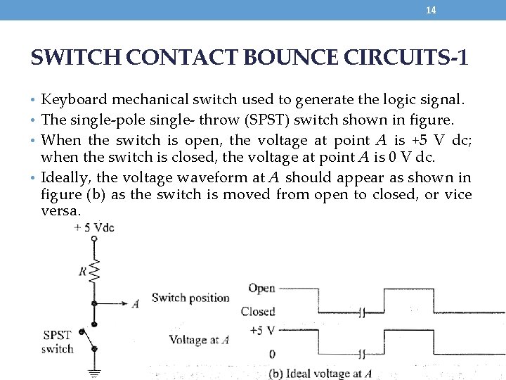
14 SWITCH CONTACT BOUNCE CIRCUITS-1 • Keyboard mechanical switch used to generate the logic signal. • The single-pole single- throw (SPST) switch shown in figure. • When the switch is open, the voltage at point A is +5 V dc; when the switch is closed, the voltage at point A is 0 V dc. • Ideally, the voltage waveform at A should appear as shown in figure (b) as the switch is moved from open to closed, or vice versa.

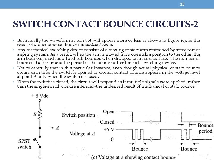
15 SWITCH CONTACT BOUNCE CIRCUITS-2 • But actually the waveform at point A will appear more or less as shown in figure (c), as the result of a phenomenon known as contact bounce. • Any mechanical switching device consists of a moving contact arm restrained by some sort of a spring system. As a result, when the arm is moved from one stable position to the other, the arm bounces, much as a hard ball bounces when dropped on a hard surface. The number of bounces that occur and the period of the bounce differ for each switching device. • Notice carefully that in this particular instance, even though actual physical contact bounce occurs each time the switch is opened or closed, contact bounce appears in the voltage level at point A only when the switch is closed. • When the switch is closed, the circuit will respond as if multiple signals were applied, rather than the single-switch closure intended-the undesired result of mechanical contact bounce.

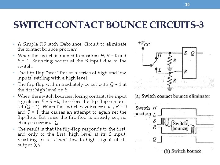
16 SWITCH CONTACT BOUNCE CIRCUITS-3 • A Simple RS latch Debounce Circuit to eliminate • • • the contact bounce problem. When the switch is moved to position H, R = 0 and S = 1. Bouncing occurs at the S input due to the switch. The flip-flop "sees" this as a series of high and low inputs, settling with a high level. The flip-flop will immediately be set with Q = 1 at the first high level on S. When the switch bounces, losing contact, the input signals are R = S = 0, therefore the flip-flop remains set (Q = 1). When the switch regains contact, R = 0 and S = 1; this causes an attempt to again set the flip-flop. But since the flip-flop is already set, no changes occur at Q. The result is that the flip-flop responds to the first, and only to the first, high level at its S input, resulting in a "clean" low-to-high signal at its output (Q).

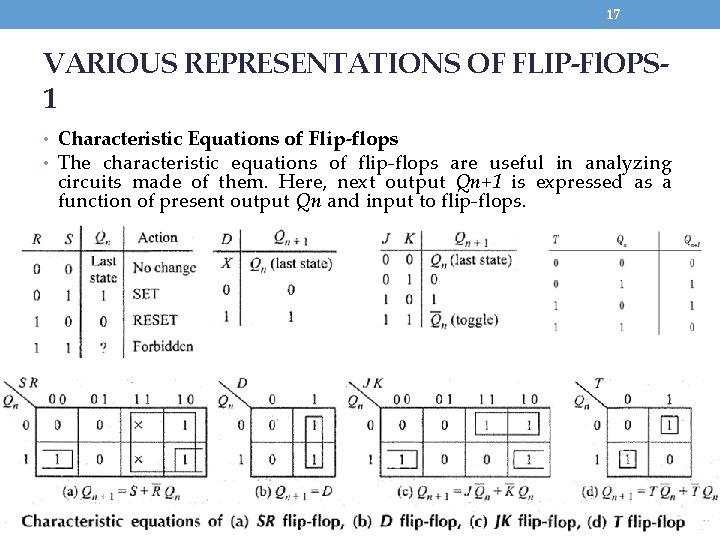
17 VARIOUS REPRESENTATIONS OF FLIP-Fl. OPS 1 • Characteristic Equations of Flip-flops • The characteristic equations of flip-flops are useful in analyzing circuits made of them. Here, next output Qn+1 is expressed as a function of present output Qn and input to flip-flops.

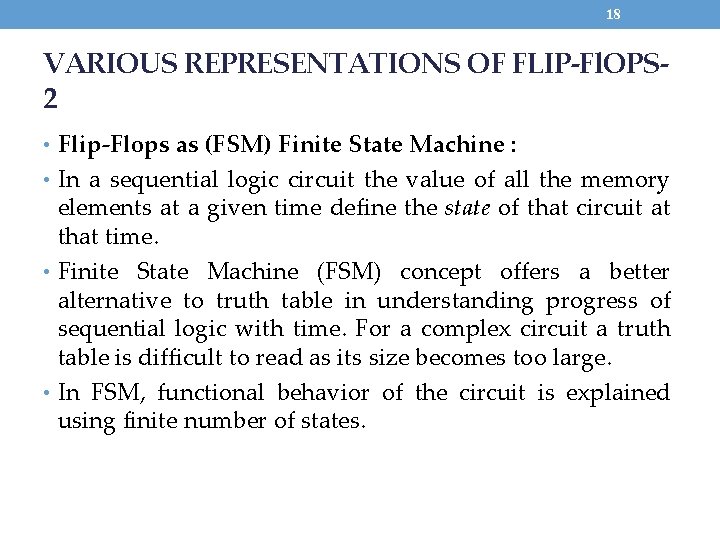
18 VARIOUS REPRESENTATIONS OF FLIP-Fl. OPS 2 • Flip-Flops as (FSM) Finite State Machine : • In a sequential logic circuit the value of all the memory elements at a given time define the state of that circuit at that time. • Finite State Machine (FSM) concept offers a better alternative to truth table in understanding progress of sequential logic with time. For a complex circuit a truth table is difficult to read as its size becomes too large. • In FSM, functional behavior of the circuit is explained using finite number of states.

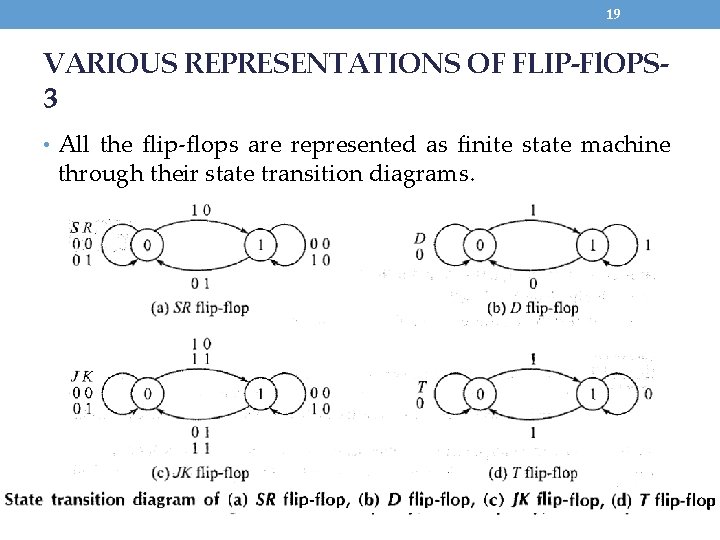
19 VARIOUS REPRESENTATIONS OF FLIP-Fl. OPS 3 • All the flip-flops are represented as finite state machine through their state transition diagrams.

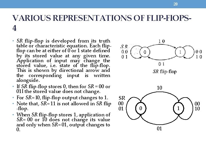
20 VARIOUS REPRESENTATIONS OF FLIP-Fl. OPS 4 • SR flip-flop is developed from its truth • • table or characteristic equation. Each flipflop can be at either of 0 or 1 state defined by its stored value at any given time. Application of input may change the stored value, i. e. state of the flip-flop. This is shown by directional arrow and the corresponding input is written alongside. If SR flip-flop stores 0, then for SR = 00 or 01 I the stored value does not change. For SR= l 0, flip-flop output changes to 1. Note that, SR= 11 is not allowed in SR flip -flop. When SR flip-flop stores 1, application of SR= 00 or 10 does not change its value and only when SR= 01, output changes to 0. 10 SR 00 01 0 1 01 00 10

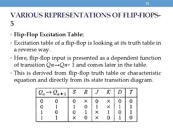
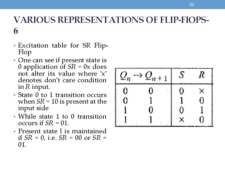
21 VARIOUS REPRESENTATIONS OF FLIP-Fl. OPS 5 • Flip-Flop Excitation Table: • Excitation table of a flip-flop is looking at its truth table in a reverse way. • Here, flip-flop input is presented as a dependent function of transition Qn→Qn+ 1 and comes later in the table. • This is derived from flip-flop truth table or characteristic equation and directly from its state transition diagram.

22 VARIOUS REPRESENTATIONS OF FLIP-Fl. OPS 6 • Excitation table for SR Flip • • Flop One can see if present state is 0 application of SR = 0 x does not alter its value where 'x' denotes don't care condition in R input. State 0 to 1 transition occurs when SR = 10 is present at the input side While state 1 to 0 transition occurs if SR = 01. Present state l is maintained if SR = 0, i. e. SR = 00 or SR = 01.

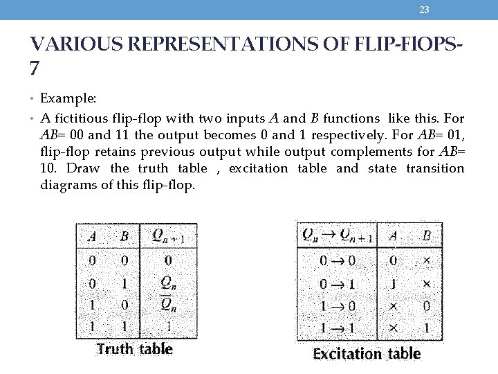
23 VARIOUS REPRESENTATIONS OF FLIP-Fl. OPS 7 • Example: • A fictitious flip-flop with two inputs A and B functions like this. For AB= 00 and 11 the output becomes 0 and 1 respectively. For AB= 01, flip-flop retains previous output while output complements for AB= 10. Draw the truth table , excitation table and state transition diagrams of this flip-flop.

24 HDL Implementation of FLIP-FLOP-1 • Use behavioural model is preferred for sequential circuit and always keyword is used in all these circuits. • For any flip-flop if EN = 1, output changes according to equation and if EN = 0, output does not change, i. e. remains latched to previous value.

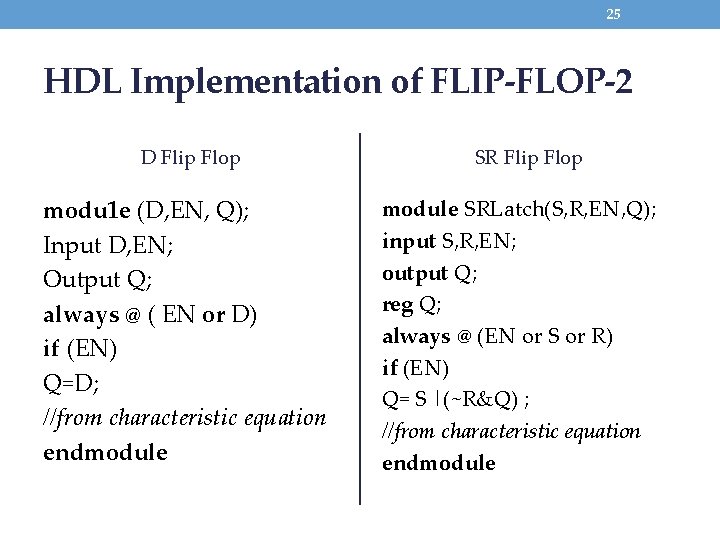
25 HDL Implementation of FLIP-FLOP-2 D Flip Flop modu 1 e (D, EN, Q); Input D, EN; Output Q; always @ ( EN or D) if (EN) Q=D; //from characteristic equation endmodule SR Flip Flop module SRLatch(S, R, EN, Q); input S, R, EN; output Q; reg Q; always @ (EN or S or R) if (EN) Q= S |(~R&Q) ; //from characteristic equation endmodule

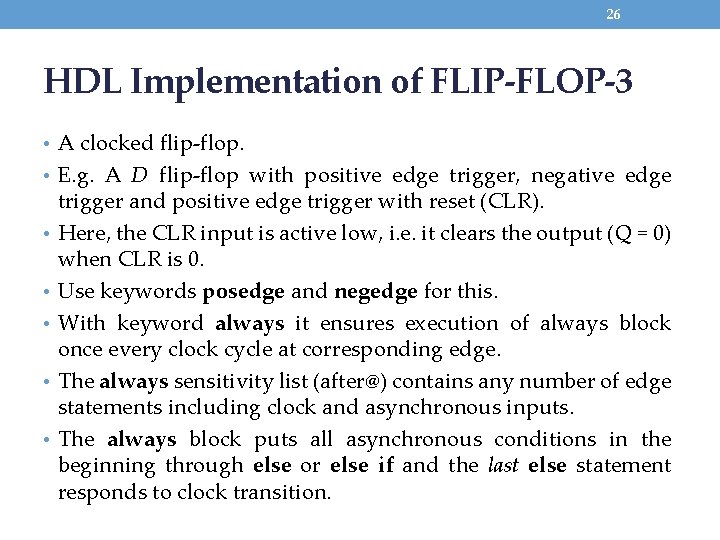
26 HDL Implementation of FLIP-FLOP-3 • A clocked flip-flop. • E. g. A D flip-flop with positive edge trigger, negative edge • • • trigger and positive edge trigger with reset (CLR). Here, the CLR input is active low, i. e. it clears the output (Q = 0) when CLR is 0. Use keywords posedge and negedge for this. With keyword always it ensures execution of always block once every clock cycle at corresponding edge. The always sensitivity list (after@) contains any number of edge statements including clock and asynchronous inputs. The always block puts all asynchronous conditions in the beginning through else or else if and the last else statement responds to clock transition.

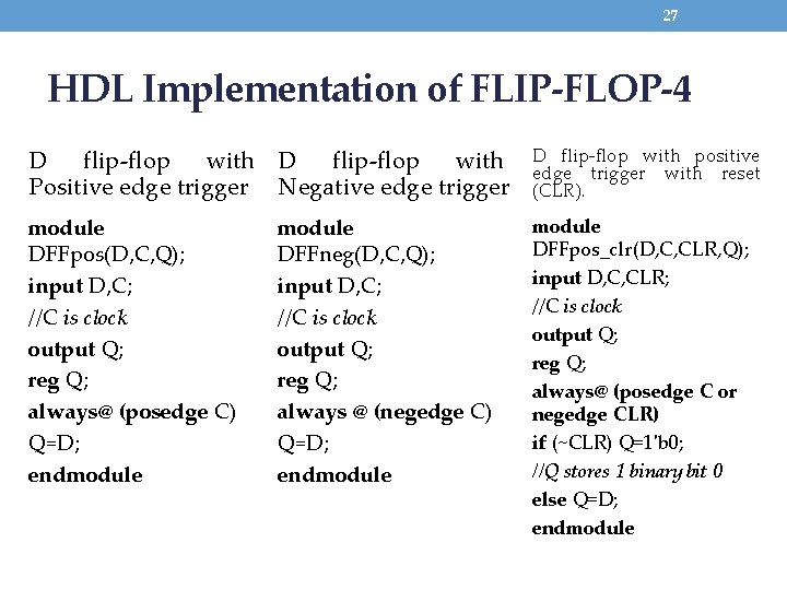
27 HDL Implementation of FLIP-FLOP-4 D flip-flop with Positive edge trigger Negative edge trigger D flip-flop with positive edge trigger with reset (CLR). module DFFpos(D, C, Q); input D, C; //C is clock output Q; reg Q; always@ (posedge C) Q=D; endmodule DFFpos_clr(D, C, CLR, Q); input D, C, CLR; //C is clock output Q; reg Q; always@ (posedge C or negedge CLR) if (~CLR) Q=1'b 0; //Q stores 1 binary bit 0 else Q=D; endmodule DFFneg(D, C, Q); input D, C; //C is clock output Q; reg Q; always @ (negedge C) Q=D; endmodule

28 • Go through the Solved and Unsolved problems from Text Book

29 REGISTERS

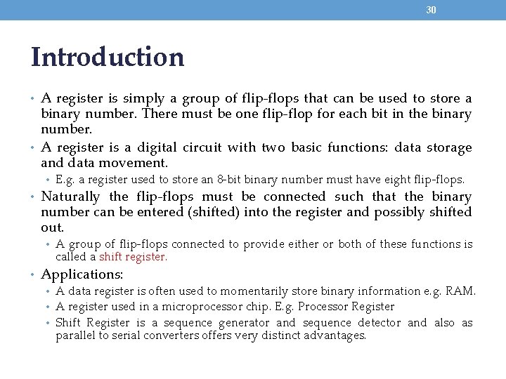
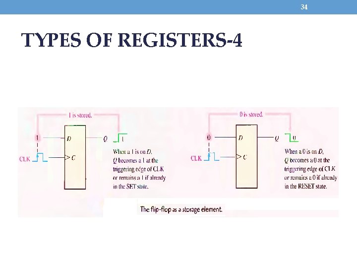
30 Introduction • A register is simply a group of flip-flops that can be used to store a binary number. There must be one flip-flop for each bit in the binary number. • A register is a digital circuit with two basic functions: data storage and data movement. • E. g. a register used to store an 8 -bit binary number must have eight flip-flops. • Naturally the flip-flops must be connected such that the binary number can be entered (shifted) into the register and possibly shifted out. • A group of flip-flops connected to provide either or both of these functions is called a shift register. • Applications: • A data register is often used to momentarily store binary information e. g. RAM. • A register used in a microprocessor chip. E. g. Processor Register • Shift Register is a sequence generator and sequence detector and also as parallel to serial converters offers very distinct advantages.

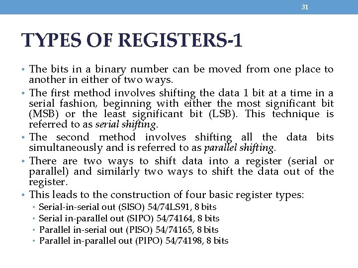
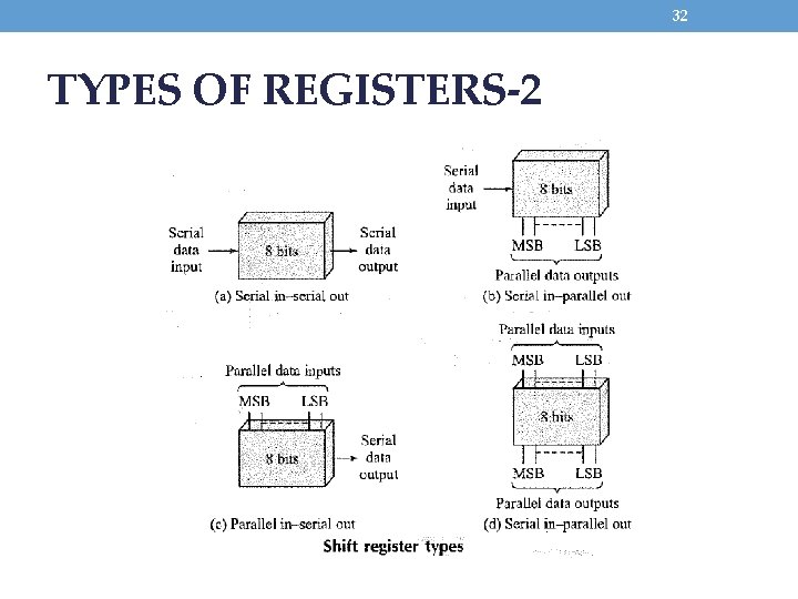
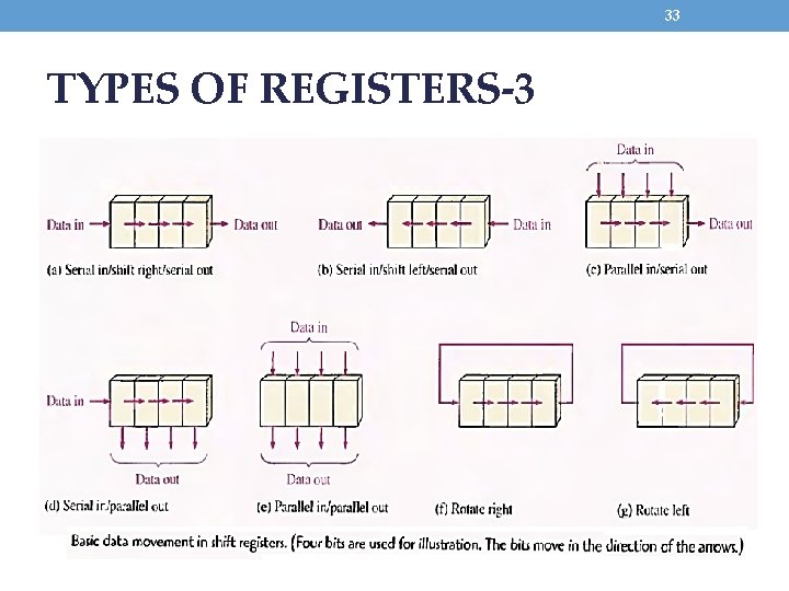
31 TYPES OF REGISTERS-1 • The bits in a binary number can be moved from one place to • • another in either of two ways. The first method involves shifting the data 1 bit at a time in a serial fashion, beginning with either the most significant bit (MSB) or the least significant bit (LSB). This technique is referred to as serial shifting. The second method involves shifting all the data bits simultaneously and is referred to as parallel shifting. There are two ways to shift data into a register (serial or parallel) and similarly two ways to shift the data out of the register. This leads to the construction of four basic register types: • • Serial-in-serial out (SISO) 54/74 LS 91, 8 bits Serial in-parallel out (SIPO) 54/74164, 8 bits Parallel in-serial out (PISO) 54/74165, 8 bits Parallel in-parallel out (PIPO) 54/74198, 8 bits

32 TYPES OF REGISTERS-2

33 TYPES OF REGISTERS-3

34 TYPES OF REGISTERS-4

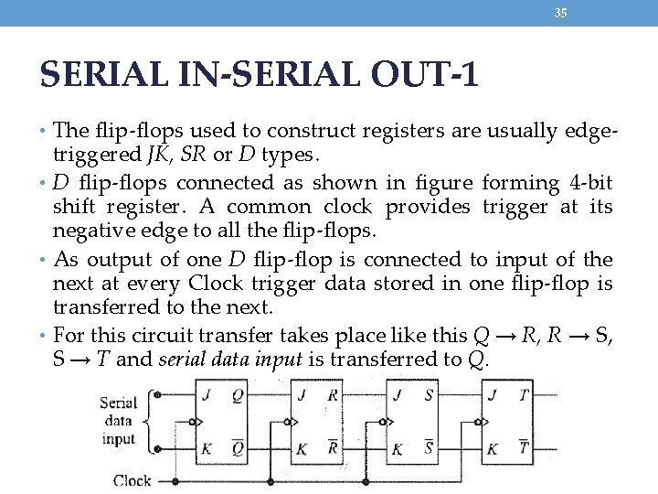
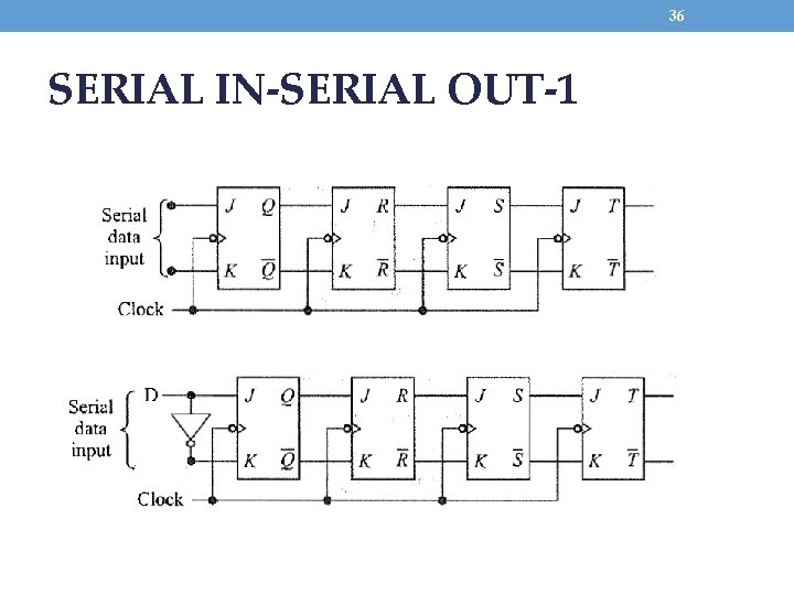
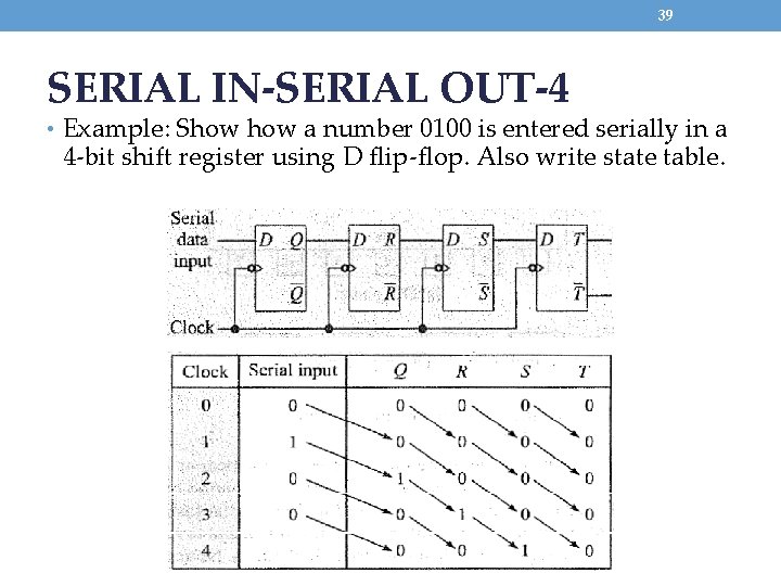
35 SERIAL IN-SERIAL OUT-1 • The flip-flops used to construct registers are usually edge- triggered JK, SR or D types. • D flip-flops connected as shown in figure forming 4 -bit shift register. A common clock provides trigger at its negative edge to all the flip-flops. • As output of one D flip-flop is connected to input of the next at every Clock trigger data stored in one flip-flop is transferred to the next. • For this circuit transfer takes place like this Q → R, R → S, S → T and serial data input is transferred to Q.

36 SERIAL IN-SERIAL OUT-1

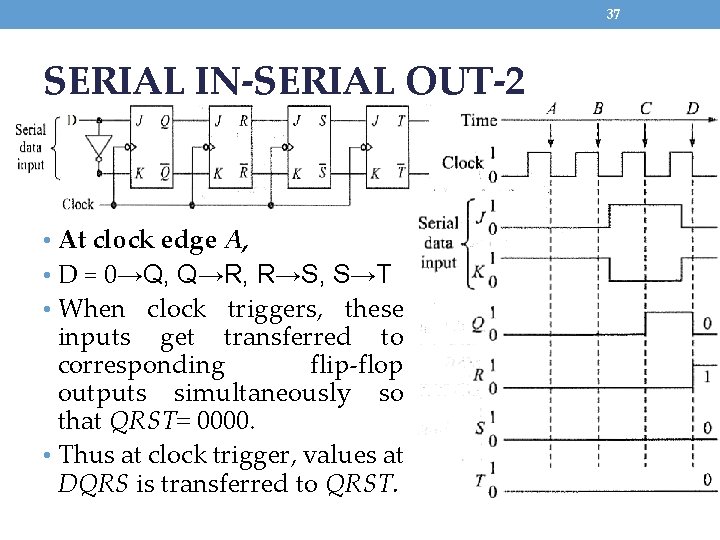
37 SERIAL IN-SERIAL OUT-2 • At clock edge A, • D = 0→Q, Q→R, R→S, S→T • When clock triggers, these inputs get transferred to corresponding flip-flop outputs simultaneously so that QRST= 0000. • Thus at clock trigger, values at DQRS is transferred to QRST.

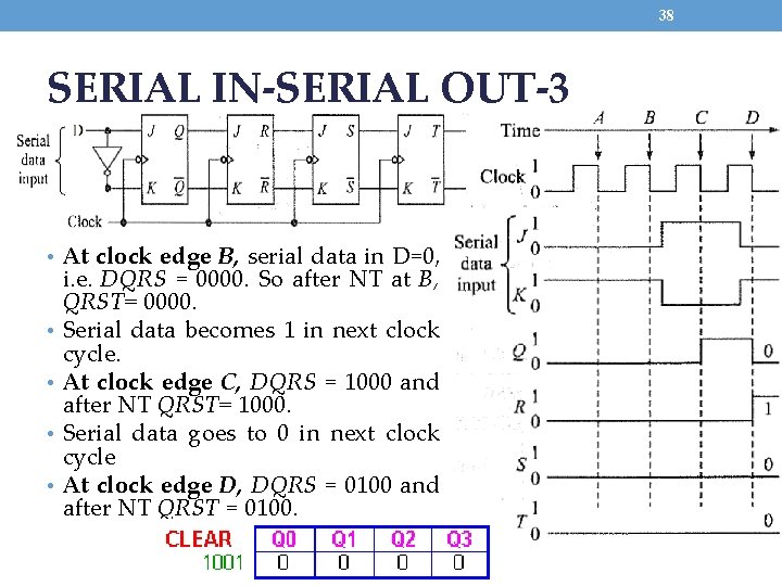
38 SERIAL IN-SERIAL OUT-3 • At clock edge B, serial data in D=0, • • i. e. DQRS = 0000. So after NT at B, QRST= 0000. Serial data becomes 1 in next clock cycle. At clock edge C, DQRS = 1000 and after NT QRST= 1000. Serial data goes to 0 in next clock cycle At clock edge D, DQRS = 0100 and after NT QRST = 0100.

39 SERIAL IN-SERIAL OUT-4 • Example: Show a number 0100 is entered serially in a 4 -bit shift register using D flip-flop. Also write state table.

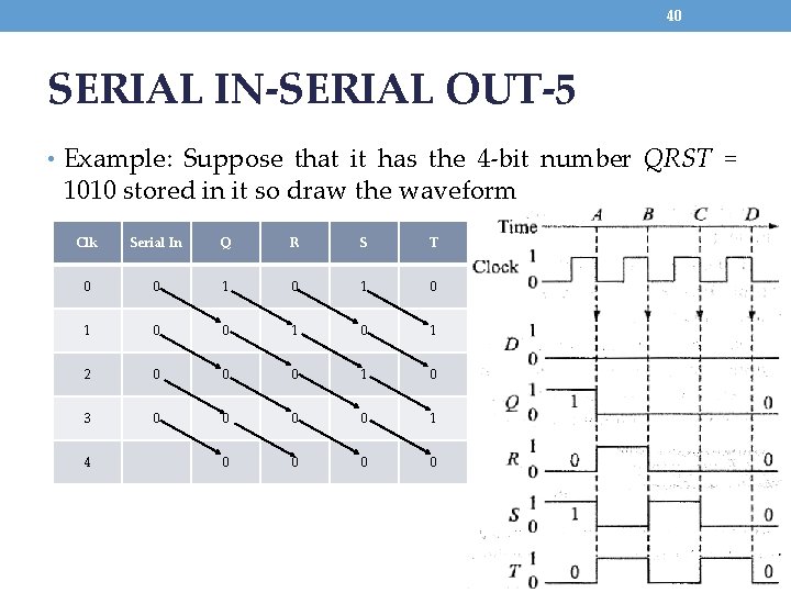
40 SERIAL IN-SERIAL OUT-5 • Example: Suppose that it has the 4 -bit number QRST = 1010 stored in it so draw the waveform Clk Serial In Q R S T 0 0 1 0 1 0 1 2 0 0 0 1 0 3 0 0 1 0 0 4

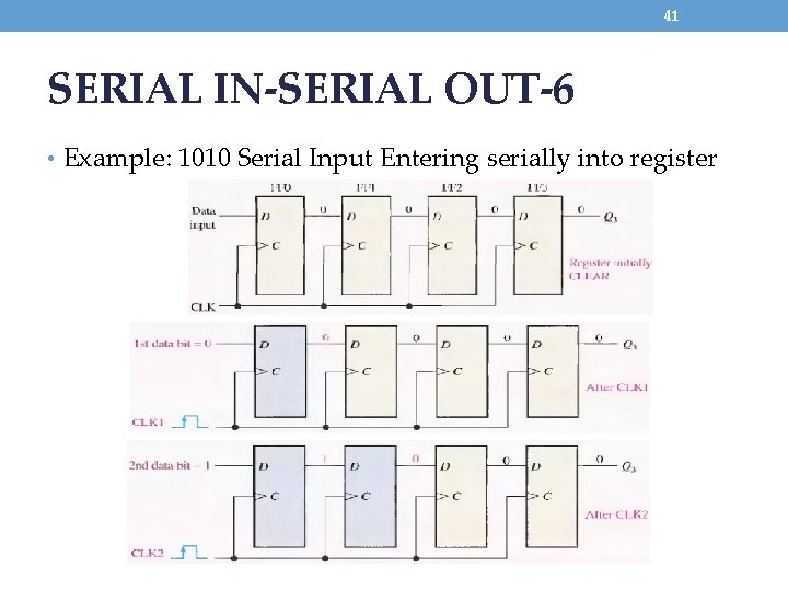
41 SERIAL IN-SERIAL OUT-6 • Example: 1010 Serial Input Entering serially into register

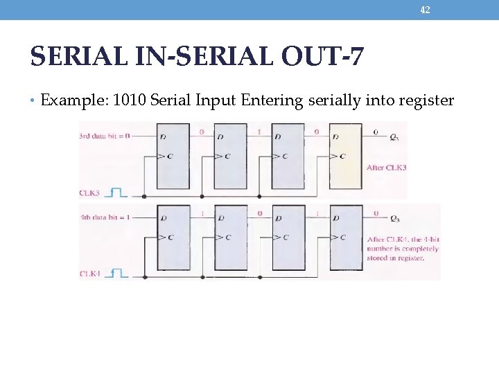
42 SERIAL IN-SERIAL OUT-7 • Example: 1010 Serial Input Entering serially into register

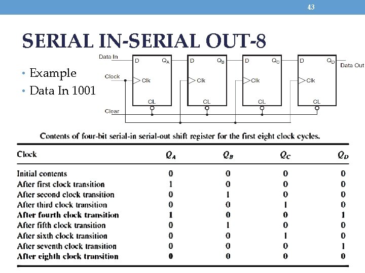
43 SERIAL IN-SERIAL OUT-8 • Example • Data In 1001

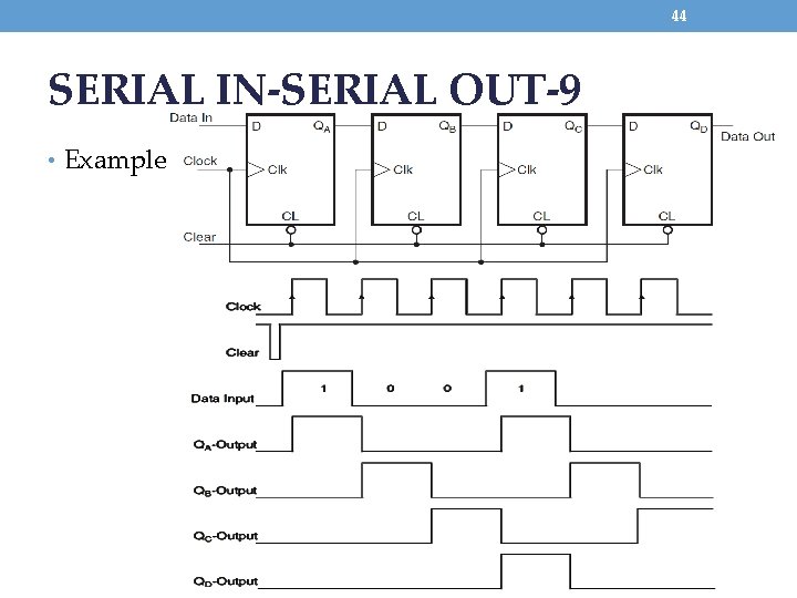
44 SERIAL IN-SERIAL OUT-9 • Example

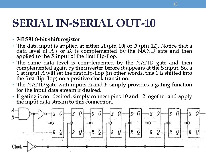
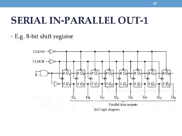
45 SERIAL IN-SERIAL OUT-10 • 74 LS 91 8 -bit shift register • The data input is applied at either A (pin 10) or B (pin 12). Notice that a data level at A ( or B) is complemented by the NAND gate and then applied to the R input of the first flip-flop. • The same data level is complemented by the NAND gate and then complemented again by the inverter before it appears at the S input. So, a 1 at input A will set the first flip-flop (in other words, this 1 is shifted into the first flip-flop) on a positive clock transition. • The NAND gate with inputs A and B simply provides a gating function for the input data stream if desired. • If gating is not desired, simply connect pins 10 and 12 together and apply the input data stream to this connection.

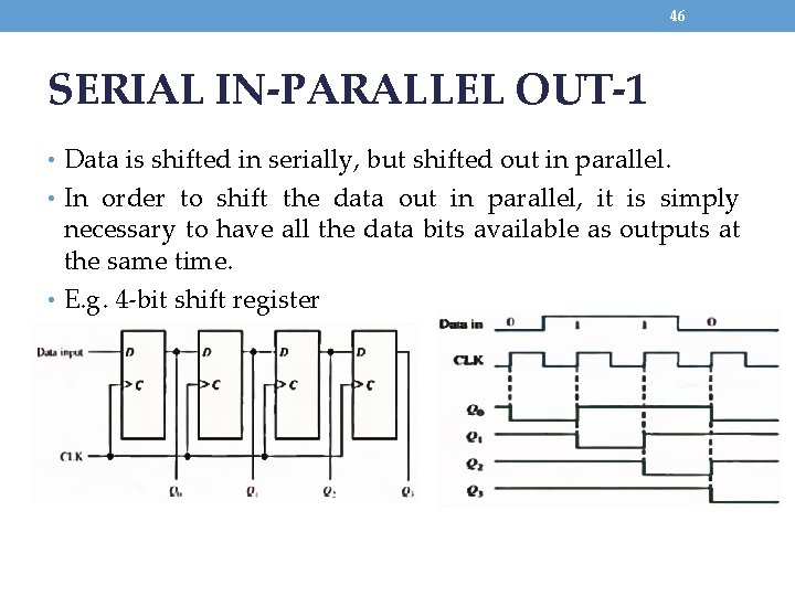
46 SERIAL IN-PARALLEL OUT-1 • Data is shifted in serially, but shifted out in parallel. • In order to shift the data out in parallel, it is simply necessary to have all the data bits available as outputs at the same time. • E. g. 4 -bit shift register

47 SERIAL IN-PARALLEL OUT-1 • E. g. 8 -bit shift register

48 SERIAL IN-PARALLEL OUT-2 • How long will it take to shift an 8 -bit number into a 8 -bit shift register if the clock is set at 10 MHz? • A minimum of eight clock periods will be required since the data is entered serially. One clock period is 100 ns, so it will require 800 ns minimum.

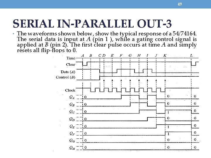
49 SERIAL IN-PARALLEL OUT-3 • The waveforms shown below, show the typical response of a 54/74164. The serial data is input at A (pin 1 ), while a gating control signal is applied at B (pin 2). The first clear pulse occurs at time A and simply resets all flip-flops to 0.

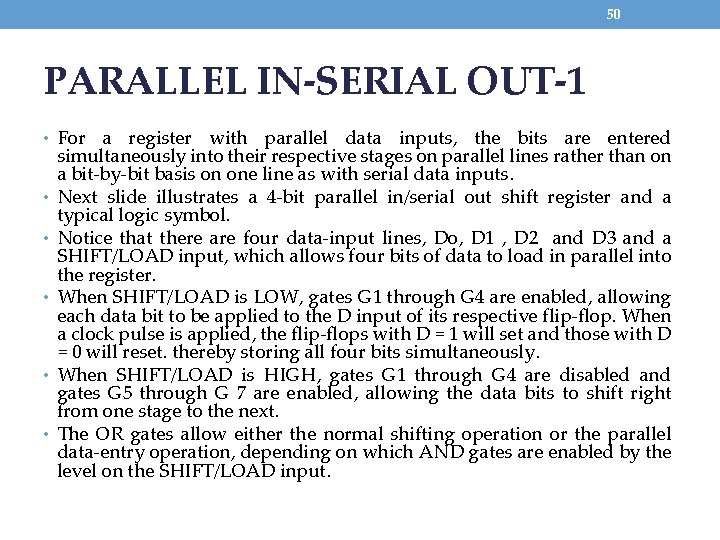
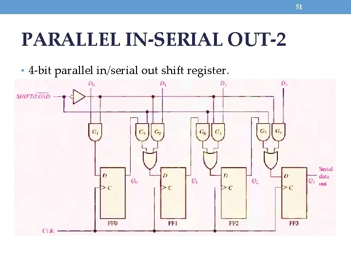
50 PARALLEL IN-SERIAL OUT-1 • For • • • a register with parallel data inputs, the bits are entered simultaneously into their respective stages on parallel lines rather than on a bit-by-bit basis on one line as with serial data inputs. Next slide illustrates a 4 -bit parallel in/serial out shift register and a typical logic symbol. Notice that there are four data-input lines, Do, D 1 , D 2 and D 3 and a SHIFT/LOAD input, which allows four bits of data to load in parallel into the register. When SHIFT/LOAD is LOW, gates G 1 through G 4 are enabled, allowing each data bit to be applied to the D input of its respective flip-flop. When a clock pulse is applied, the flip-flops with D = 1 will set and those with D = 0 will reset. thereby storing all four bits simultaneously. When SHIFT/LOAD is HIGH, gates G 1 through G 4 are disabled and gates G 5 through G 7 are enabled, allowing the data bits to shift right from one stage to the next. The OR gates allow either the normal shifting operation or the parallel data-entry operation, depending on which AND gates are enabled by the level on the SHIFT/LOAD input.

51 PARALLEL IN-SERIAL OUT-2 • 4 -bit parallel in/serial out shift register.

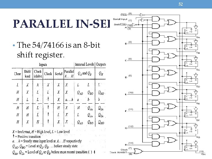
52 PARALLEL IN-SERIAL OUT-3 • The 54/74166 is an 8 -bit shift register.

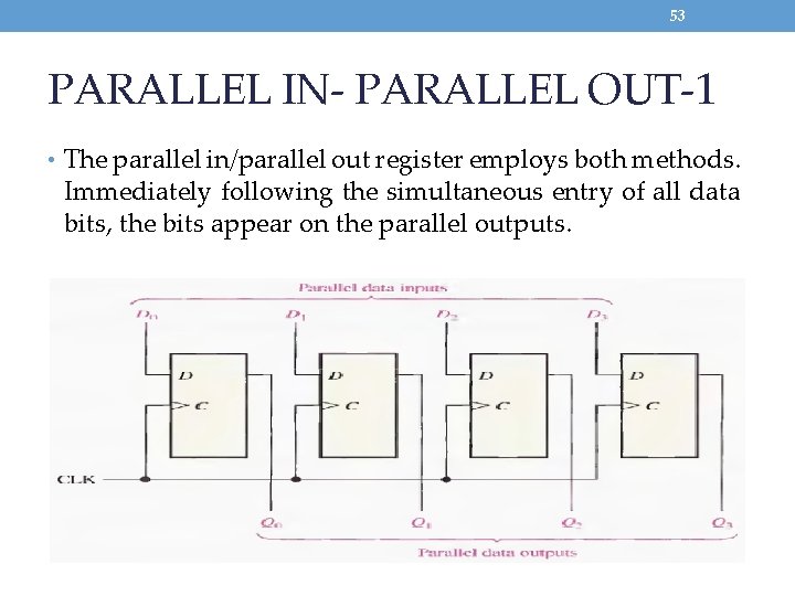
53 PARALLEL IN- PARALLEL OUT-1 • The parallel in/parallel out register employs both methods. Immediately following the simultaneous entry of all data bits, the bits appear on the parallel outputs.

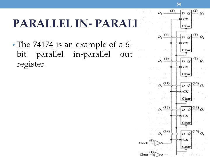
54 PARALLEL IN- PARALLEL OUT-2 • The 74174 is an example of a 6 - bit parallel register. in-parallel out

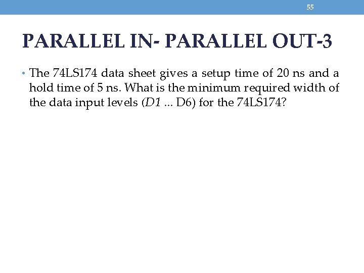
55 PARALLEL IN- PARALLEL OUT-3 • The 74 LS 174 data sheet gives a setup time of 20 ns and a hold time of 5 ns. What is the minimum required width of the data input levels (D 1. . . D 6) for the 74 LS 174?

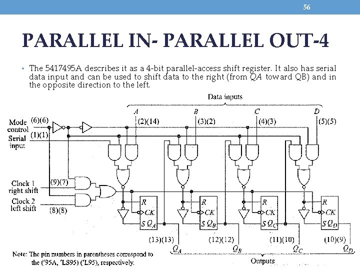
56 PARALLEL IN- PARALLEL OUT-4 • The 5417495 A describes it as a 4 -bit parallel-access shift register. It also has serial data input and can be used to shift data to the right (from QA toward QB) and in the opposite direction to the left.

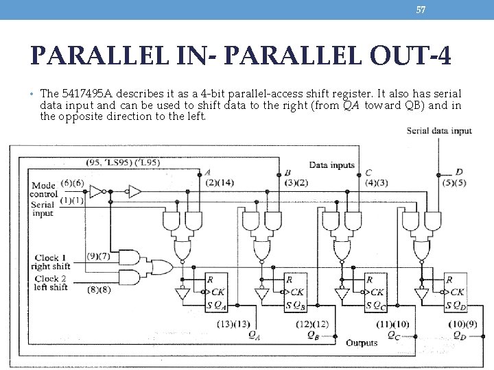
57 PARALLEL IN- PARALLEL OUT-4 • The 5417495 A describes it as a 4 -bit parallel-access shift register. It also has serial data input and can be used to shift data to the right (from QA toward QB) and in the opposite direction to the left.

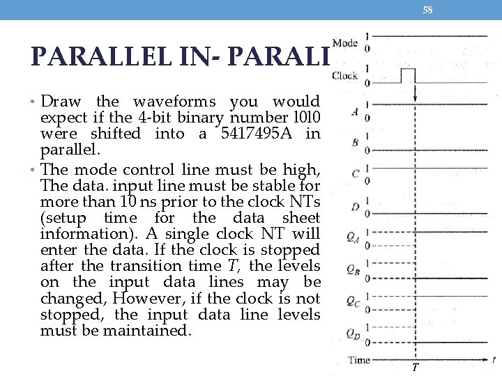
58 PARALLEL IN- PARALLEL OUT-5 • Draw the waveforms you would expect if the 4 -bit binary number l 0 l 0 were shifted into a 5417495 A in parallel. • The mode control line must be high, The data. input line must be stable for more than 10 ns prior to the clock NTs (setup time for the data sheet information). A single clock NT will enter the data. If the clock is stopped after the transition time T, the levels on the input data lines may be changed, However, if the clock is not stopped, the input data line levels must be maintained.

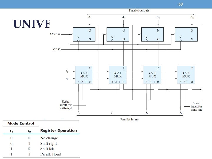
59 UNIVERSAL SHIFT REGISTER-1 • Basic types of shift register , the following operations are possible-serial in-serial out, serial in-parallel out, parallel in-serial out, and parallel in-parallel out. Serial in or serial out again can be made possible by shifting data in any of the two directions, left shift (QA←QB←QC←QD←Data in) and right shift (Data in→QA→QB→QC→QD). A universal shift register can perform all the four operations and is also bidirectional in nature.

60 UNIVERSAL SHIFT REGISTER-2

61 APPLICATIONS Of SHIFT REGISTERS-1 • Shift register can be used to count number of pulses entering into a system as ring counter or switched-tail counter. As ring counter it can generate various control signals in a sequential manner. • Shift register can also generate a prescribed sequence repetitively or detect a particular sequence from data input. It can also help in reduction of hardware by converting parallel data feed to serial one. • Serial adder is one such application discussed in this section.

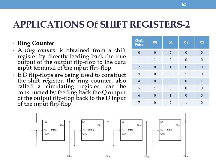
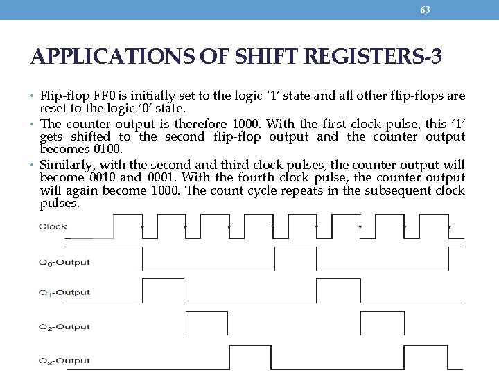
62 APPLICATIONS Of SHIFT REGISTERS-2 • Ring Counter • A ring counter is obtained from a shift register by directly feeding back the true output of the output flip-flop to the data input terminal of the input flip-flop. • If D flip-flops are being used to construct the shift register, the ring counter, also called a circulating register, can be constructed by feeding back the Q output of the output flip-flop back to the D input of the input flip-flop. Clock Pulse Q 0 Q 1 Q 2 Q 3 0 0 0 1 1 0 0 0 2 0 1 0 0 3 0 0 1 0 4 0 0 0 1 5 1 0 0 0 6 0 1 0 0 7 0 0 1 0

63 APPLICATIONS OF SHIFT REGISTERS-3 • Flip-flop FF 0 is initially set to the logic ‘ 1’ state and all other flip-flops are reset to the logic ‘ 0’ state. • The counter output is therefore 1000. With the first clock pulse, this ‘ 1’ gets shifted to the second flip-flop output and the counter output becomes 0100. • Similarly, with the second and third clock pulses, the counter output will become 0010 and 0001. With the fourth clock pulse, the counter output will again become 1000. The count cycle repeats in the subsequent clock pulses.

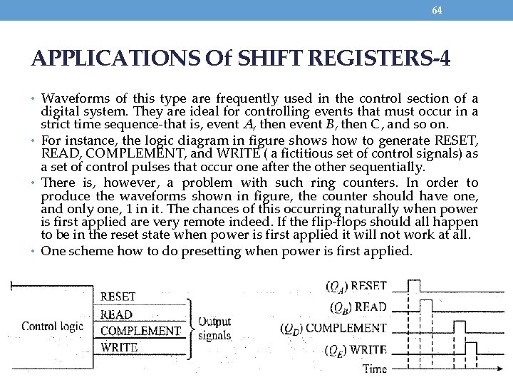
64 APPLICATIONS Of SHIFT REGISTERS-4 • Waveforms of this type are frequently used in the control section of a digital system. They are ideal for controlling events that must occur in a strict time sequence-that is, event A, then event B, then C, and so on. • For instance, the logic diagram in figure shows how to generate RESET, READ, COMPLEMENT, and WRITE ( a fictitious set of control signals) as a set of control pulses that occur one after the other sequentially. • There is, however, a problem with such ring counters. In order to produce the waveforms shown in figure, the counter should have one, and only one, 1 in it. The chances of this occurring naturally when power is first applied are very remote indeed. If the flip-flops should all happen to be in the reset state when power is first applied it will not work at all. • One scheme how to do presetting when power is first applied.

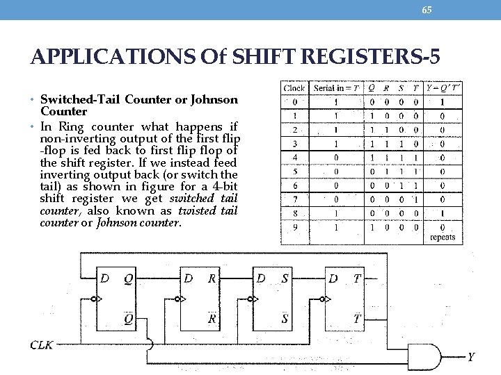
65 APPLICATIONS Of SHIFT REGISTERS-5 • Switched-Tail Counter or Johnson Counter • In Ring counter what happens if non-inverting output of the first flip -flop is fed back to first flip flop of the shift register. If we instead feed inverting output back (or switch the tail) as shown in figure for a 4 -bit shift register we get switched tail counter, also known as twisted tail counter or Johnson counter.

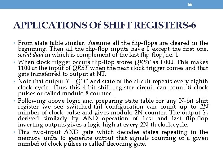
66 APPLICATIONS Of SHIFT REGISTERS-6 • From state table similar. Assume all the flip-flops are cleared in the • • beginning. Then all the flip-flop inputs have 0 except the first one, serial data in which is complement of the last flip-flop, i. e. 1. When clock trigger occurs flip-flop stores QRST as I 000. This makes 1100 at the input of QRST when the next clock trigger comes and that gets transferred to output at NT. Note that output Y = Q'T' and state of the circuit repeats every eighth clock cycle. Thus this 4 -bit shift register circuit can count 8 clock pulses or called modulo-8 counter. Following above logic and preparing state table for any N-bit shift register we see switched-tail configuration can count up to 2 N number of clock pulse and gives modulo-2 N counter. The output Y, derived similarly by AND operation of first and last flip-flop inverting outputs gives a logic high at every 2 N-th clock cycle. This two-input AND gate which decodes states repeating in the memory units to generate output that signals counting of a given number of clock pulses is called decoding gate.

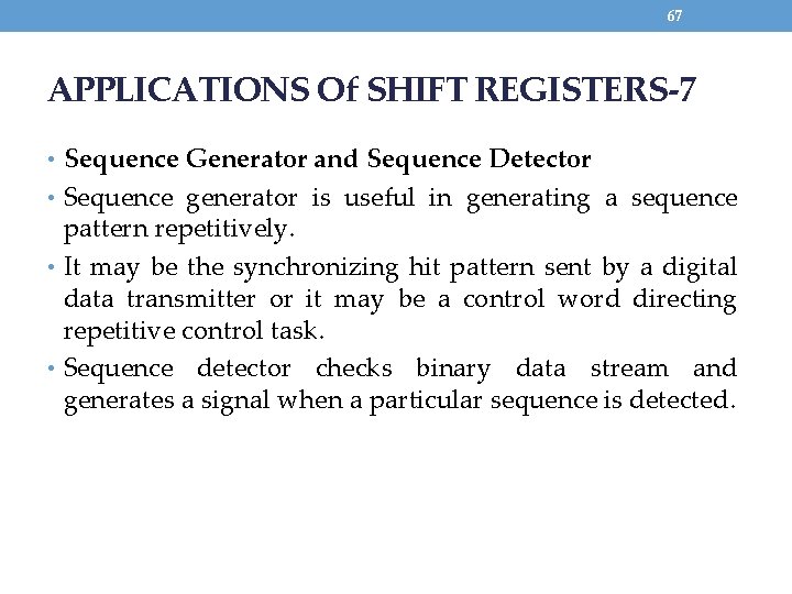
67 APPLICATIONS Of SHIFT REGISTERS-7 • Sequence Generator and Sequence Detector • Sequence generator is useful in generating a sequence pattern repetitively. • It may be the synchronizing hit pattern sent by a digital data transmitter or it may be a control word directing repetitive control task. • Sequence detector checks binary data stream and generates a signal when a particular sequence is detected.

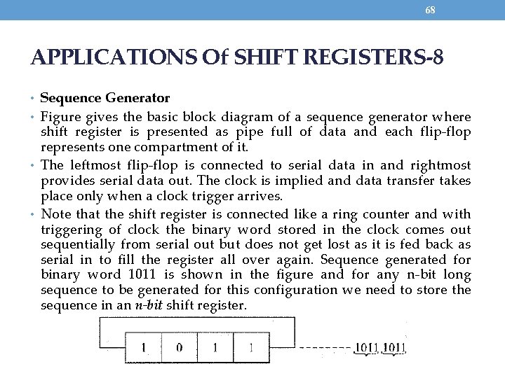
68 APPLICATIONS Of SHIFT REGISTERS-8 • Sequence Generator • Figure gives the basic block diagram of a sequence generator where shift register is presented as pipe full of data and each flip-flop represents one compartment of it. • The leftmost flip-flop is connected to serial data in and rightmost provides serial data out. The clock is implied and data transfer takes place only when a clock trigger arrives. • Note that the shift register is connected like a ring counter and with triggering of clock the binary word stored in the clock comes out sequentially from serial out but does not get lost as it is fed back as serial in to fill the register all over again. Sequence generated for binary word 1011 is shown in the figure and for any n-bit long sequence to be generated for this configuration we need to store the sequence in an n-bit shift register.

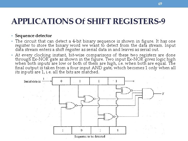
69 APPLICATIONS Of SHIFT REGISTERS-9 • Sequence detector • The circuit that can detect a 4 -bit binary sequence is shown in figure. It has one register to store the binary word we want to detect from the data stream. Input data stream enters a shift register as serial data in and leaves as serial out. • At every clocking instant, bit-wise comparisons of these two registers are done through Ex-NOR gate as shown in the figure. Two input Ex-NOR gives logic high when both inputs are low or both of them are high, i. e. when both are equal. The final output is taken from a four input AND gate, which becomes 1 only when all its inputs are 1, i. e. all the bits are matched.

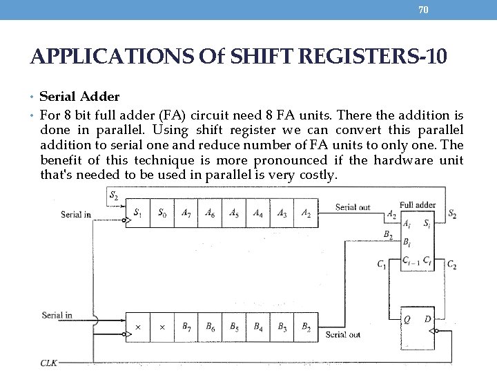
70 APPLICATIONS Of SHIFT REGISTERS-10 • Serial Adder • For 8 bit full adder (FA) circuit need 8 FA units. There the addition is done in parallel. Using shift register we can convert this parallel addition to serial one and reduce number of FA units to only one. The benefit of this technique is more pronounced if the hardware unit that's needed to be used in parallel is very costly.

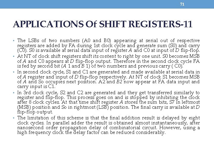
71 APPLICATIONS Of SHIFT REGISTERS-11 • The LSBs of two numbers (A 0 and B 0) appearing at serial out of respective • • registers are added by FA during 1 st clock cycle and generate sum (S 0) and carry (C 0). S 0 is available at serial data input of register A and C 0 at input of D flip-flop. At NT of clock shift registers shift its content to right by one unit. S 0 becomes MSB of A and C 0 appears at D flip-flop output. Therefore in the second clock cycle FA is fed by second bit (A 1 and B 1) of two numbers and previous carry ( C 0). In second clock cycle, S 1 and C 1 are generated and made available at serial data in of A register and input of D flip-flop respectively. At NT of clock S 1 becomes MSB of A and So occupies next position. A 2 and B 2 now appear at FA data input and carry input is C 1. In 3 rd clock cycle, S 2 and C 2 are generated and they get transferred similarly to register and flip-flop. This process goes on and is stopped by inhibiting the clock after 8 clock cycles. At that time shift register A stores the sum bits, S 7 in leftmost (MSB) position and So in rightmost (LSB) position. The final carry is available at D flip-flop output. The limitation of this scheme is that the final addition result is delayed by eight clock cycles. In parallel adder the result is obtained almost instantaneously, after nanosecond order propagation delay of combinatorial circuit. However, using a high frequency clock the delay factor can be reduced considerably.

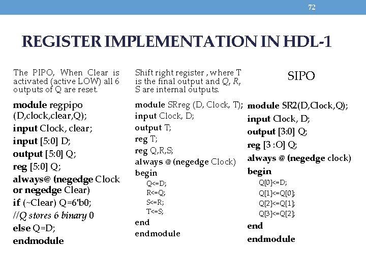
72 REGISTER IMPLEMENTATION IN HDL-1 The PIPO, When Clear is activated (active LOW) all 6 outputs of Q are reset. Shift right register , where T is the final output and Q, R, S are internal outputs. SIPO module regpipo (D, clock, clear, Q); input Clock, clear; input [5: 0] D; output [5: 0] Q; reg [5: 0] Q; always@ (negedge Clock or negedge Clear) if (~Clear) Q=6'b 0; //Q stores 6 binary 0 else Q=D; endmodule SRreg (D, Clock, T); input Clock, D; output T; reg Q, R, S; always @ (negedge Clock) begin module SR 2(D, Clock, Q); input Clock, D; output [3: 0] Q; reg [3 : O] Q; always @ (negedge clock) begin end endmodule Q<=D; R<=Q; S<=R; T<=S; Q[0]<=D; Q[1]<=Q[0]; Q[2]<=Q[1]; Q[3]<=Q[2];

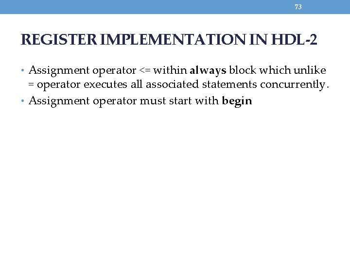
73 REGISTER IMPLEMENTATION IN HDL-2 • Assignment operator <= within always block which unlike = operator executes all associated statements concurrently. • Assignment operator must start with begin

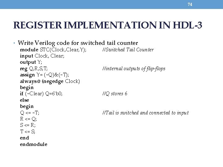
74 REGISTER IMPLEMENTATION IN HDL-3 • Write Verilog code for switched tail counter module STC(Clock, Clear, Y); //Switched Tail Counter input Clock, Clear; output Y; reg Q, R, S, T; //internal outputs of flip-flops assign Y= (~Q)&(~T); always@ (negedge Clock) begin if (~Clear) Q=6'b 0; //Q stores 6 else begin Q <= ~T; //Tail is switched and connected to input R <= Q; S <= R; T <= S; endmodule

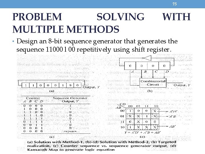
75 PROBLEM SOLVING MULTIPLE METHODS WITH • Design an 8 -bit sequence generator that generates the sequence 11000 l 00 repetitively using shift register.

76 COUNTERS

77 Introduction • A counter driven by a clock can be used to count the number of • • • clock cycles. Since the clock pulses occur at known intervals, the counter can be used as an instrument for measuring time and therefore period or frequency. There are basically two different types of counters-synchronous and asynchronous. Serial, or asynchronous counter is defined as each flip-flop is triggered by the previous flip-flop, and thus the counter has a cumulative settling time. An increase in speed of operation can be achieved by use of a parallel or synchronous counter. Here, every flip-flop is triggered by the clock (in synchronism), and thus settling time is simply equal to the delay time of a single flip-flop. Serial and parallel counters are used in combination to compromise between speed of operation and hardware count.

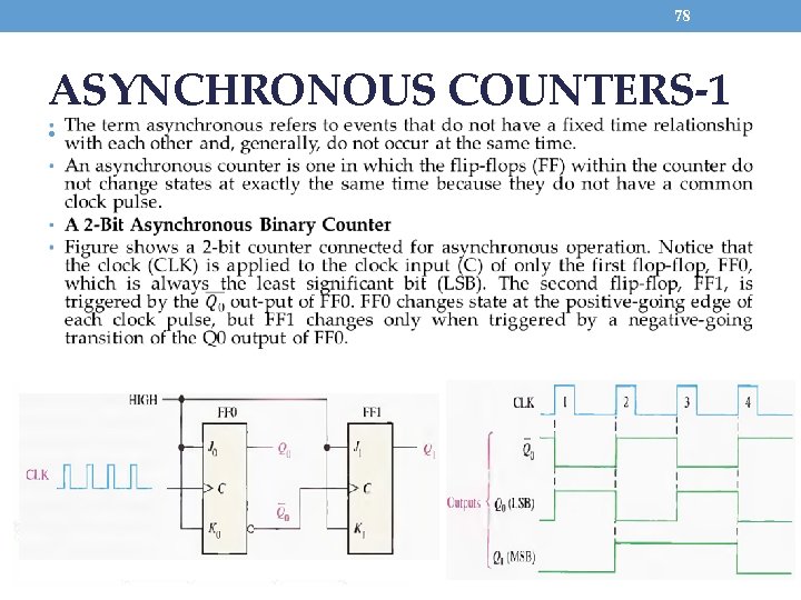
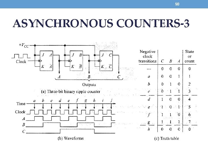
78 ASYNCHRONOUS COUNTERS-1 •

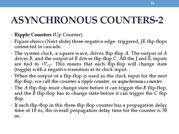
79 ASYNCHRONOUS COUNTERS-2 • Ripple Counters (Up Counter) • Figure shows (Next slide) three negative edge- triggered, JK flip-flops • • connected in cascade. The system clock, a square wave, drives flip-flop A. The output of A drives B, and the output of B drives flip-flop C. All the J and K inputs are tied to +VCC· This means that each flip-flop will change state (toggle) with a negative transition at its clock input. When the output of a flip-flop is used as the clock input for the next flip-flop, we call the counter a ripple counter, or asynchronous counter. The A flip-flop must change state before it can trigger the B flip-flop, and the B flip-flop has to change state before it can trigger the C flipflop. If each flip-flop in this three-flip-flop counter has a propagation delay time of 10 ns, the overall propagation delay time for the counter is 30 ns.

80 ASYNCHRONOUS COUNTERS-3

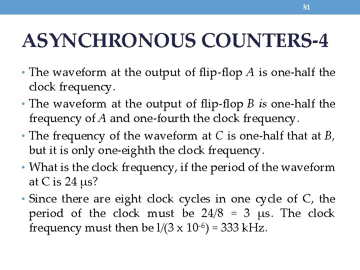
81 ASYNCHRONOUS COUNTERS-4 • The waveform at the output of flip-flop A is one-half the clock frequency. • The waveform at the output of flip-flop B is one-half the frequency of A and one-fourth the clock frequency. • The frequency of the waveform at C is one-half that at B, but it is only one-eighth the clock frequency. • What is the clock frequency, if the period of the waveform at C is 24 μs? • Since there are eight clock cycles in one cycle of C, the period of the clock must be 24/8 = 3 μs. The clock frequency must then be l/(3 x 10 -6) = 333 k. Hz.

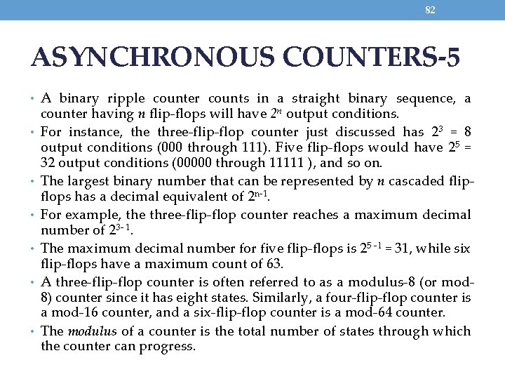
82 ASYNCHRONOUS COUNTERS-5 • A binary ripple counter counts in a straight binary sequence, a • • • counter having n flip-flops will have 2 n output conditions. For instance, the three-flip-flop counter just discussed has 23 = 8 output conditions (000 through 111). Five flip-flops would have 25 = 32 output conditions (00000 through 11111 ), and so on. The largest binary number that can be represented by n cascaded flipflops has a decimal equivalent of 2 n-1. For example, the three-flip-flop counter reaches a maximum decimal number of 23 - 1. The maximum decimal number for five flip-flops is 25 - l = 31, while six flip-flops have a maximum count of 63. A three-flip-flop counter is often referred to as a modulus-8 (or mod 8) counter since it has eight states. Similarly, a four-flip-flop counter is a mod-16 counter, and a six-flip-flop counter is a mod-64 counter. The modulus of a counter is the total number of states through which the counter can progress.

83 ASYNCHRONOUS COUNTERS-6 • How many flip-flops are required to construct a mod- 128 counter? A mod-32? What is the largest decimal number that can be stored in a mod-64 counter? • A mod-128 counter must have seven flip-flols, since 27 = 128. • Five flip-flops are needed to construct a mod-32 counter. • The largest decima 1 number that can be stored in a six-flop flip counter (mod-64) is 111111 = 63. • Note carefully the difference between the modulus ( total number of states) and the maximum decimal number.

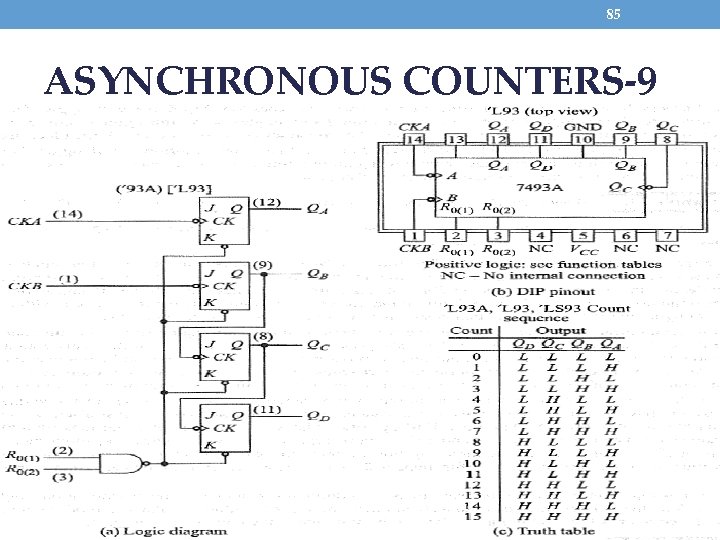
84 ASYNCHRONOUS COUNTERS-8 • The 54/7493 A • A 4 -bit binary counter that can be used in either a mod-8 or a mod-16 configuration. If the clock is applied at input CKB, the outputs will appear at QB, QC, and QD, and this is a mod-8 binary ripple counter. • If the clock is applied at input CKA and flip-flop QA is connected to input CKB, have a mod-16, 4 -bit binary ripple counter. The outputs are QA, QB, QC, and QD.

85 ASYNCHRONOUS COUNTERS-9

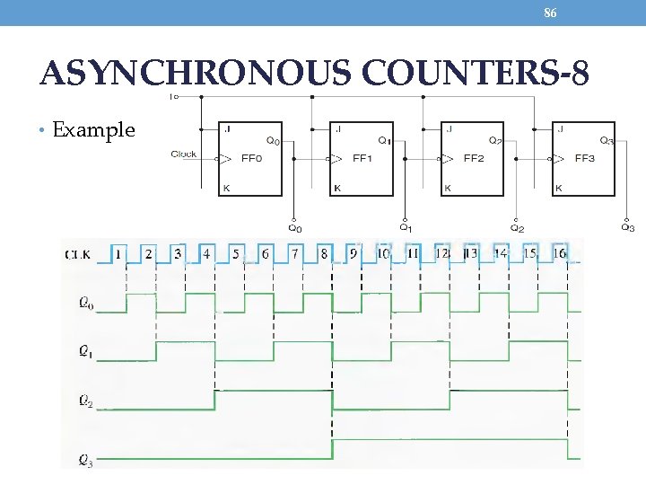
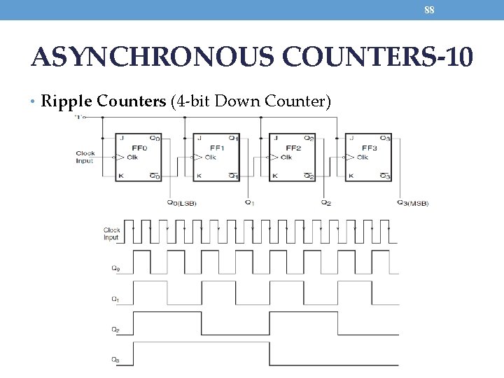
86 ASYNCHRONOUS COUNTERS-8 • Example

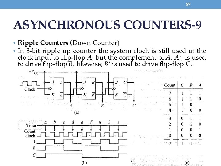
87 ASYNCHRONOUS COUNTERS-9 • Ripple Counters (Down Counter) • In 3 -bit ripple up counter the system clock is still used at the clock input to flip-flop A, but the complement of A, A’, is used to drive flip-flop B, likewise; B’ is used to drive flip-flop C.

88 ASYNCHRONOUS COUNTERS-10 • Ripple Counters (4 -bit Down Counter)

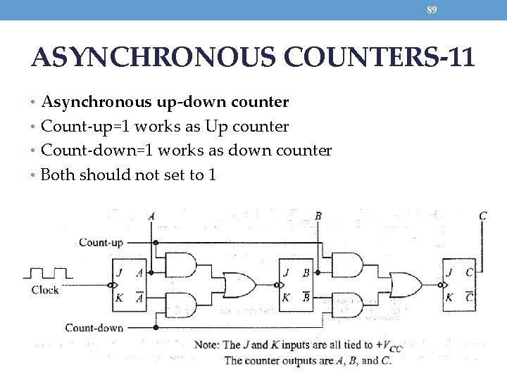
89 ASYNCHRONOUS COUNTERS-11 • Asynchronous up-down counter • Count-up=1 works as Up counter • Count-down=1 works as down counter • Both should not set to 1

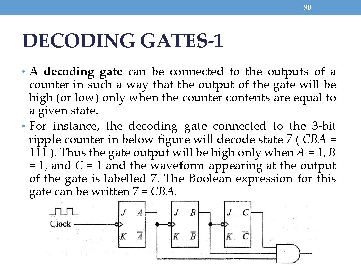
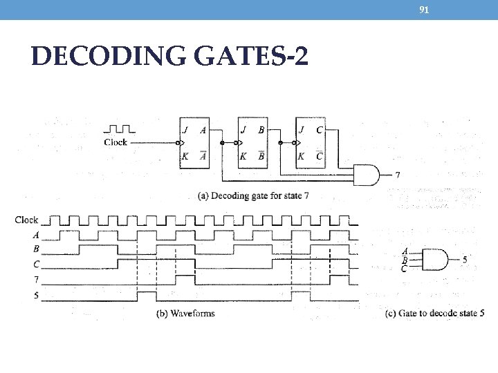
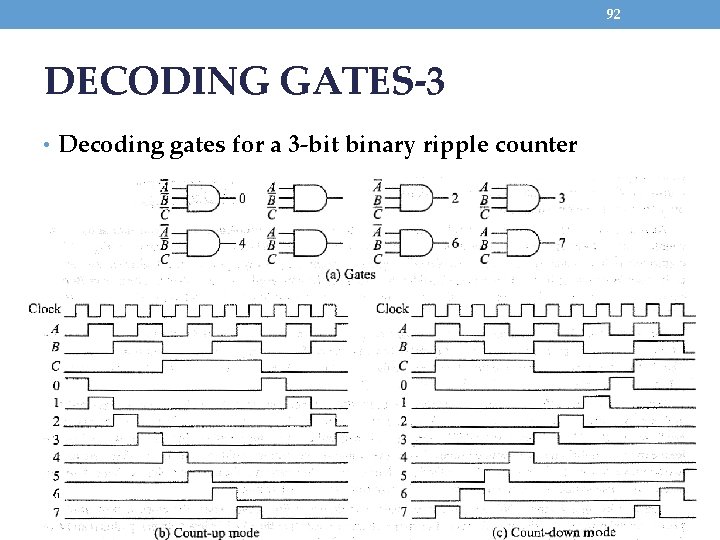
90 DECODING GATES-1 • A decoding gate can be connected to the outputs of a counter in such a way that the output of the gate will be high (or low) only when the counter contents are equal to a given state. • For instance, the decoding gate connected to the 3 -bit ripple counter in below figure will decode state 7 ( CBA = 111 ). Thus the gate output will be high only when A = 1, B = 1, and C = 1 and the waveform appearing at the output of the gate is labelled 7. The Boolean expression for this gate can be written 7 = CBA.

91 DECODING GATES-2

92 DECODING GATES-3 • Decoding gates for a 3 -bit binary ripple counter

93 SYNCHRONOUS COUNTERS-1 • The ripple counter is the simplest to build, but there is a limit to • • • its highest operating frequency. As each flip-flop has a delay time. In a ripple counter these delay times are additive, and the total "settling" time for the counter is approximately the delay times the total number of flip-flops. There is the possibility of glitches occurring at the output of decoding gates used with a ripple counter. To overcome by the use of a synchronous parallel counter. The main difference here is that every flip-flop is triggered in synchronism with the clock. The term synchronous refers to events that have a fixed time relationship with each other. A synchronous counter is one in which all the flip-flops in the counter are clocked at the same time by a common clock pulse.

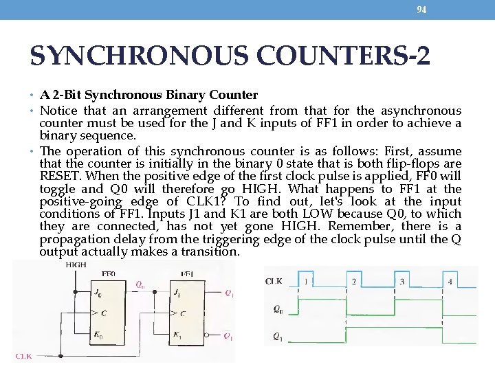
94 SYNCHRONOUS COUNTERS-2 • A 2 -Bit Synchronous Binary Counter • Notice that an arrangement different from that for the asynchronous counter must be used for the J and K inputs of FF 1 in order to achieve a binary sequence. • The operation of this synchronous counter is as follows: First, assume that the counter is initially in the binary 0 state that is both flip-flops are RESET. When the positive edge of the first clock pulse is applied, FF 0 will toggle and Q 0 will therefore go HIGH. What happens to FF 1 at the positive-going edge of CLK 1? To find out, let's look at the input conditions of FF 1. Inputs J 1 and K 1 are both LOW because Q 0, to which they are connected, has not yet gone HIGH. Remember, there is a propagation delay from the triggering edge of the clock pulse until the Q output actually makes a transition.

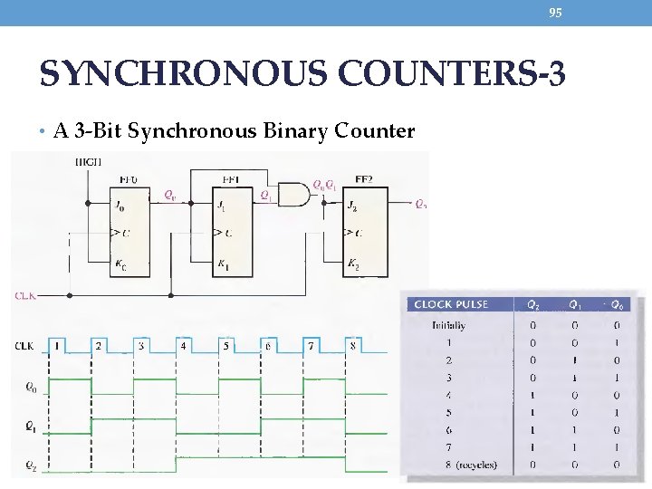
95 SYNCHRONOUS COUNTERS-3 • A 3 -Bit Synchronous Binary Counter

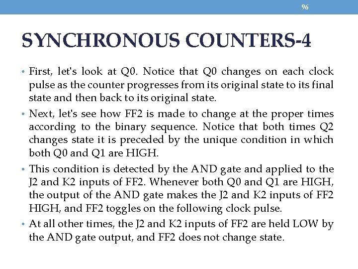
96 SYNCHRONOUS COUNTERS-4 • First, let's look at Q 0. Notice that Q 0 changes on each clock pulse as the counter progresses from its original state to its final state and then back to its original state. • Next, let's see how FF 2 is made to change at the proper times according to the binary sequence. Notice that both times Q 2 changes state it is preceded by the unique condition in which both Q 0 and Q 1 are HIGH. • This condition is detected by the AND gate and applied to the J 2 and K 2 inputs of FF 2. Whenever both Q 0 and Q 1 are HIGH, the output of the AND gate makes the J 2 and K 2 inputs of FF 2 HIGH, and FF 2 toggles on the following clock pulse. • At all other times, the J 2 and K 2 inputs of FF 2 are held LOW by the AND gate output, and FF 2 does not change state.

97 SYNCHRONOUS COUNTERS-4 • Each flip-flop should have its J and K inputs connected such that they are HIGH only when the outputs of all lower order flip-flops are in the HIGH state.

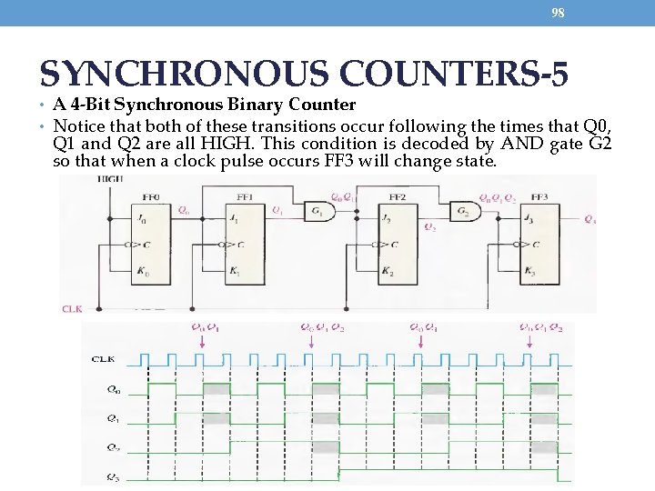
98 SYNCHRONOUS COUNTERS-5 • A 4 -Bit Synchronous Binary Counter • Notice that both of these transitions occur following the times that Q 0, Q 1 and Q 2 are all HIGH. This condition is decoded by AND gate G 2 so that when a clock pulse occurs FF 3 will change state.

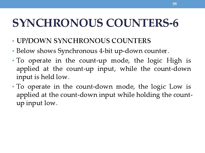
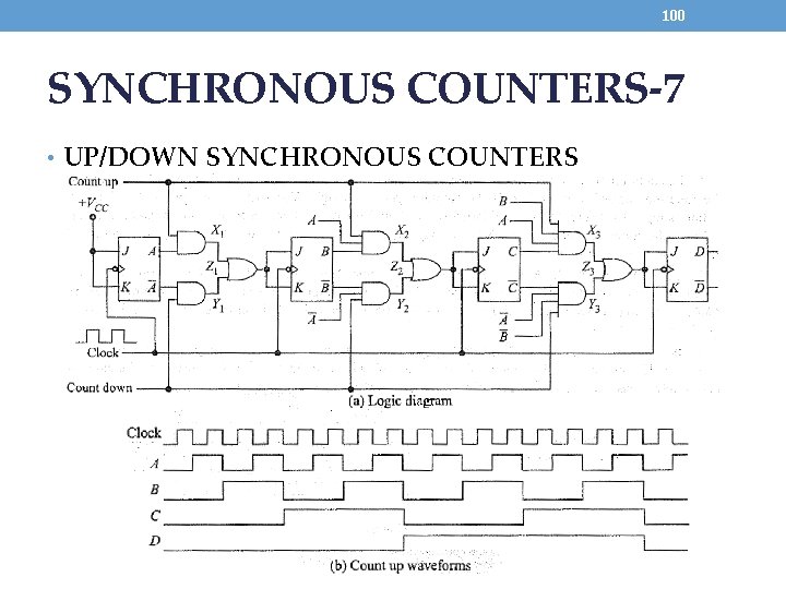
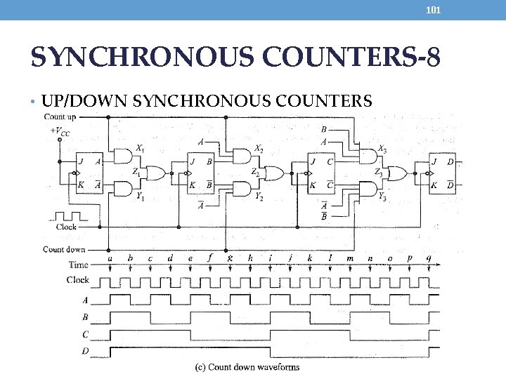
99 SYNCHRONOUS COUNTERS-6 • UP/DOWN SYNCHRONOUS COUNTERS • Below shows Synchronous 4 -bit up-down counter. • To operate in the count-up mode, the logic High is applied at the count-up input, while the count-down input is held low. • To operate in the count-down mode, the logic Low is applied at the count-down input while holding the countup input low.

100 SYNCHRONOUS COUNTERS-7 • UP/DOWN SYNCHRONOUS COUNTERS

101 SYNCHRONOUS COUNTERS-8 • UP/DOWN SYNCHRONOUS COUNTERS

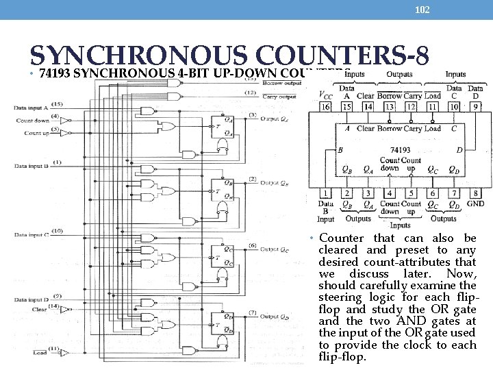
102 SYNCHRONOUS COUNTERS-8 74193 SYNCHRONOUS 4 -BIT UP-DOWN COUNTERS • • Counter that can also be cleared and preset to any desired count-attributes that we discuss later. Now, should carefully examine the steering logic for each flipflop and study the OR gate and the two AND gates at the input of the OR gate used to provide the clock to each flip-flop.

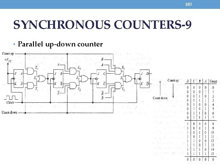
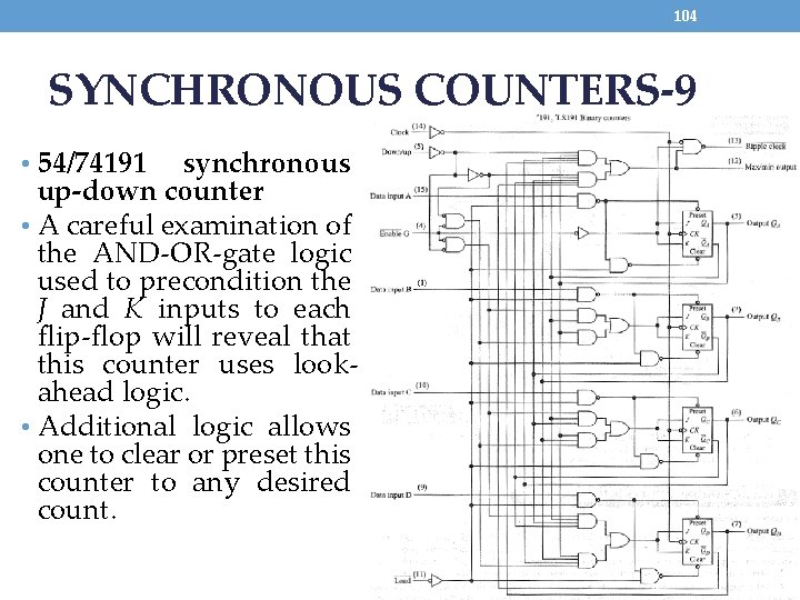
103 SYNCHRONOUS COUNTERS-9 • Parallel up-down counter

104 SYNCHRONOUS COUNTERS-9 • 54/74191 synchronous up-down counter • A careful examination of the AND-OR-gate logic used to precondition the J and K inputs to each flip-flop will reveal that this counter uses lookahead logic. • Additional logic allows one to clear or preset this counter to any desired count.

105 CHANGING THE COUNTER MODULUS-1 • Counter Modulus • A modulus given by 2 n, where n indicates the number of flip-flops. Such counters • • • are said to have a "natural count" of 2 n. A mod-2 counter consists of a single flip-flop; a mod-4 counter requires two flipflops, and it counts through four discrete states. Three flip-flops form a mod-8 counter, while four flip-flops form a mod-16 counter. Thus we can construct counters that have a natural count of 2, 4, 8, 16, 32, and so on by using the proper number of flip-flops. It is often desirable to construct counters having a modulus other than 2, 4, 8, and so on. For example, a counter having a modulus of 3, or 5, would be useful. A small modulus counter can always be constructed from a larger modulus counter by skipping states. Such counters are said to have a modified count. It is first necessary to determine the number of flip-flops required. The correct number of flip-flops is determined choosing the lowest natural count that is greater than the desired modified count. For example, a mod-7 counter requires three flip-flops, since 8 is the lowest natural count greater than the desired modified count of 7. • MOD number = 2 N • where N is the number of flip-flops connected

106 CHANGING THE COUNTER MODULUS-2 • Question • Indicate how many flip-flops are required to construct each of the following counters: (a) mod-3, (b) mod-6, and (c) mod-9. • The lowest natural count greater than 3 is 4. Two flip-flops provide a natural count of 4. Therefore, it requires at least two flip-flops to construct a mod-3 counter. • Construction of a mod-6 counter requires at least three flip-flops, since 8 is the lowest natural count greater than 6. • A mod-9 counter requires at least four flip-flops, since 16 is the lowest natural count greater than 9.

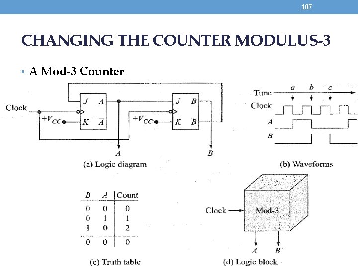
107 CHANGING THE COUNTER MODULUS-3 • A Mod-3 Counter

108 CHANGING THE COUNTER MODULUS-4 • A Mod-3 Counter • Above circuit considered as a divide-by-3 block, since the output waveform at B ( or at A) has a period equal to three times that of the clock-in other words, this counter • divides the clock frequency by 3.

109 CHANGING THE COUNTER MODULUS-5 • If we consider a basic flip-flop to be a mod-2 counter, we see that a mod-4 counter (two flip-flops in series) is simply two mod-2 counters in series. • Similarly, a mod-8 counter is simply a 2 x 2 connection, and so on. • Thus a great number of higher-modulus counters can be formed by using the product of any number of lower modulus counters.

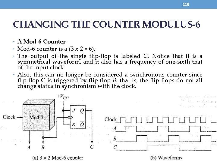
110 CHANGING THE COUNTER MODULUS-6 • A Mod-6 Counter • Mod-6 counter is a (3 x 2 = 6). • The output of the single flip-flop is labeled C. Notice that it is a symmetrical waveform, and it also has a frequency of one-sixth that of the input clock. • Also, this can no longer be considered a synchronous counter since flip flop C is triggered by flip-flop B; that is, the flip-flops do not all change status in synchronism with the clock.

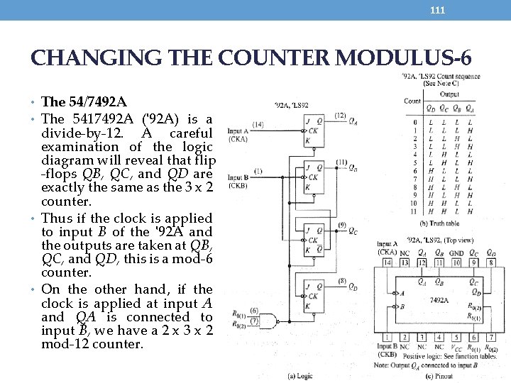
111 CHANGING THE COUNTER MODULUS-6 • The 54/7492 A • The 5417492 A ('92 A) is a divide-by-12. A careful examination of the logic diagram will reveal that flip -flops QB, QC, and QD are exactly the same as the 3 x 2 counter. • Thus if the clock is applied to input B of the '92 A and the outputs are taken at QB, QC, and QD, this is a mod-6 counter. • On the other hand, if the clock is applied at input A and QA is connected to input B, we have a 2 x 3 x 2 mod-12 counter.