COE 202 Digital Logic Design Courtesy of Dr
- Slides: 28

COE 202: Digital Logic Design Courtesy of Dr. Radwan E Abdel-Aal Logic and Computer Design Fundamentals Chapter 3 and – Combinational Registers Counters Logic Design Part 1 – Implementation Technology and Logic Design Charles Kime & Thomas Kaminski © 2004 Pearson Education, Inc. Terms of Use (Hyperlinks are active in View Show mode)

Registers and Counters Useful MSI blocks made of Flip-Flops § § Registers with Parallel Load Shift Registers Counters: Synchronous and Asynchronous Modulo Counters Chapter 3 - Part 1 2

Registers § Register – a collection of binary storage elements § In theory, a register is sequential logic, i. e. can be defined by a state table § But more often, we think of a register as an array of n flip flops (possibly with some extra gates) that store a vector of n binary bits § Used to perform simple data storage, movement, manipulation and processing operations (e. g. load, increment, shift, add, etc. ) § The computer processes data by performing operations on registers, e. g. ADD A, B where A and B are say 32 -bit registers Chapter 3 - Part 1 3

Register/Counter Design Methods § Classical Direct Approach: From State Diagram Design individual cells using the state diagram/state table model and combine them into a register § Problem: for n large number of states state diagram/state table model is often not feasible!- Pentium has 64 -bit data registers (states = ? ) § Alternative (Ad hoc? ) Approach: (similar to iterative design method in combinational logic) Add predefined combinational circuits to a register to perform desired functions § Example: To count up, connect the register flip-flop outputs to an incrementer Chapter 3 - Part 1 4

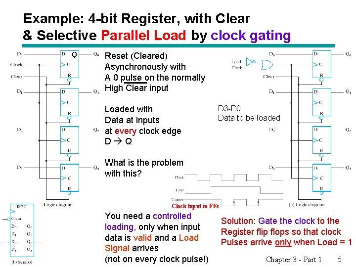
Example: 4 -bit Register, with Clear & Selective Parallel Load by clock gating Q Reset (Cleared) Asynchronously with A 0 pulse on the normally High Clear input Loaded with Data at inputs at every clock edge D Q D 3 -D 0 Data to be loaded What is the problem with this? Clock input to FFs You need a controlled loading, only when input data is valid and a Load Signal arrives (not on every clock pulse!) Solution: Gate the clock to the Register flip flops so that clock Pulses arrive only when Load = 1 Chapter 3 - Part 1 5

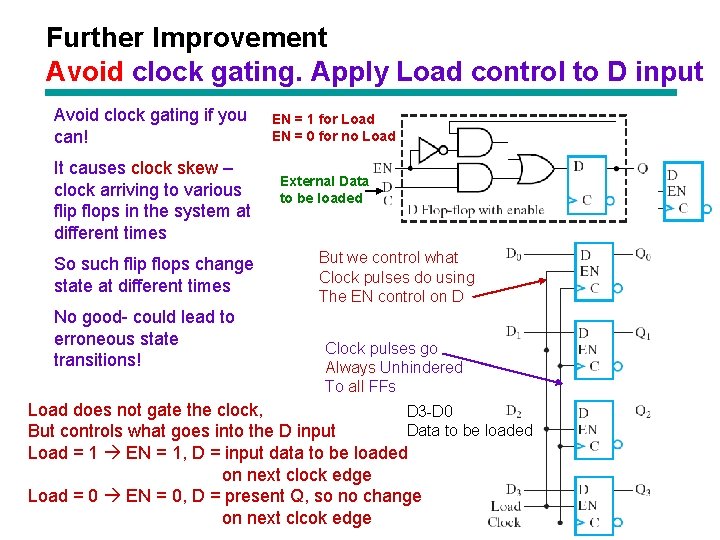
Further Improvement Avoid clock gating. Apply Load control to D input Avoid clock gating if you can! It causes clock skew – clock arriving to various flip flops in the system at different times So such flip flops change state at different times No good- could lead to erroneous state transitions! EN = 1 for Load EN = 0 for no Load External Data to be loaded But we control what Clock pulses do using The EN control on D Clock pulses go Always Unhindered To all FFs Load does not gate the clock, D 3 -D 0 Data to be loaded But controls what goes into the D input Load = 1 EN = 1, D = input data to be loaded on next clock edge Load = 0 EN = 0, D = present Q, so no change on next clcok edge Chapter 3 - Part 1 6

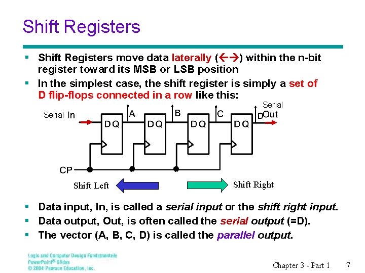
Shift Registers § Shift Registers move data laterally ( ) within the n-bit register toward its MSB or LSB position § In the simplest case, the shift register is simply a set of D flip-flops connected in a row like this: Serial D Serial Shift Left Shift Right § Data input, In, is called a serial input or the shift right input. § Data output, Out, is often called the serial output (=D). § The vector (A, B, C, D) is called the parallel output. Chapter 3 - Part 1 7

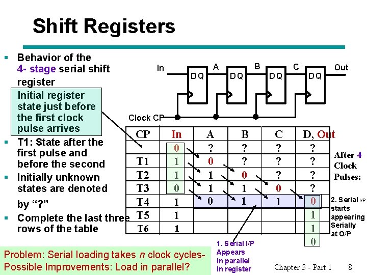
Shift Registers § Behavior of the 4 - stage serial shift register Initial register state just before the first clock pulse arrives § T 1: State after the first pulse and before the second § Initially unknown states are denoted DQ DQ C DQ DQ Out Clock CP CP T 1 T 2 T 3 T 4 by “? ” § Complete the last three T 5 rows of the table B A In T 6 In 0 1 1 A ? 0 1 1 0 B ? ? 0 1 1 1 Problem: Serial loading takes n clock cycles. Possible Improvements: Load in parallel? 1. Serial I/P Appears in parallel In register C ? ? ? 0 1 D, Out ? After 4 ? Clock ? Pulses: ? 0 2. Serial I/P starts 1 appearing 1 Serially at O/P 0 Chapter 3 - Part 1 8

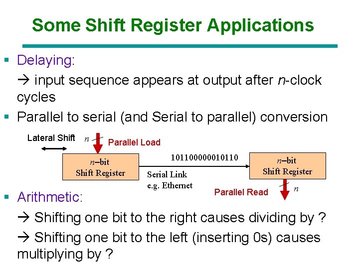
Some Shift Register Applications § Delaying: input sequence appears at output after n-clock cycles § Parallel to serial (and Serial to parallel) conversion Lateral Shift n Parallel Load n–bit Shift Register 101100000010110 Serial Link e. g. Ethernet n–bit Shift Register Parallel Read n § Arithmetic: Shifting one bit to the right causes dividing by ? Shifting one bit to the left (inserting 0 s) causes multiplying by ? Chapter 3 - Part 1 9

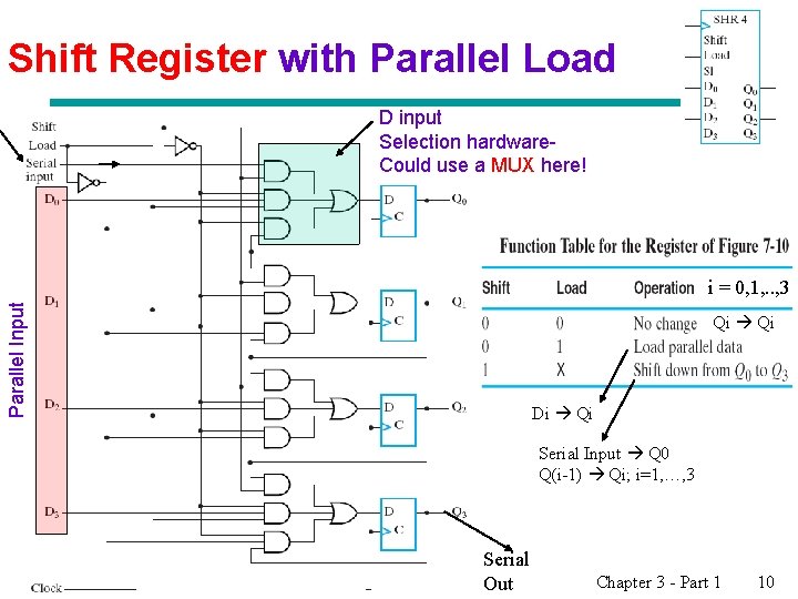
Shift Register with Parallel Load § ddd D input Selection hardware. Could use a MUX here! Parallel Input i = 0, 1, . . , 3 Qi Di Qi Serial Input Q 0 Q(i-1) Qi; i=1, …, 3 Serial Out Chapter 3 - Part 1 10

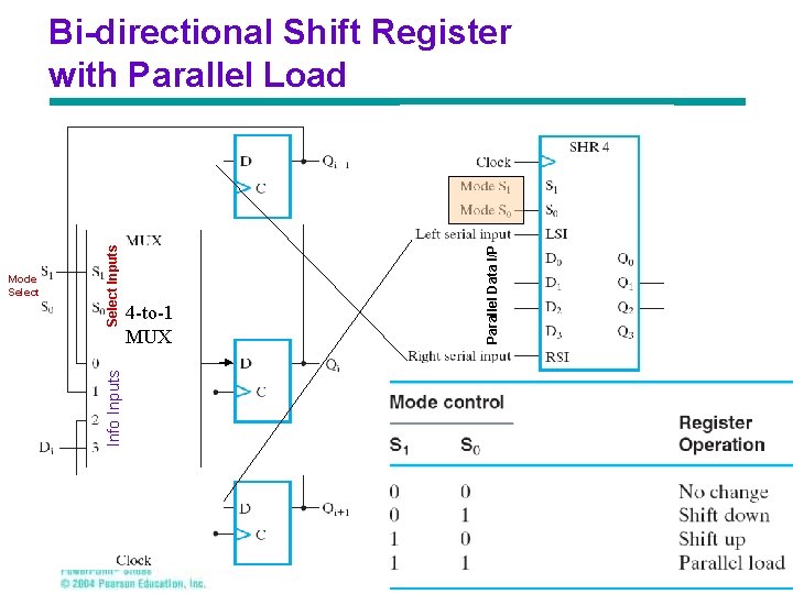
Parallel Data I/P 4 -to-1 MUX Info Inputs Mode Select Inputs Bi-directional Shift Register with Parallel Load Chapter 3 - Part 1 11

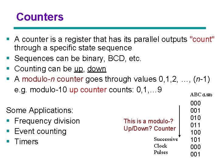
Counters § A counter is a register that has its parallel outputs "count" through a specific state sequence § Sequences can be binary, BCD, etc. § Counting can be up, down § A modulo-n counter goes through values 0, 1, 2, …, (n-1) e. g. modulo-10 up counter counts: 0, 1, … 9 ABC (LSB) Some Applications: § Frequency division § Event counting § Timers This is a modulo-? Up/Down? Counter Successive Clock Pulses 000 001 010 011 100 101 000 001 Chapter 3 - Part 1 12

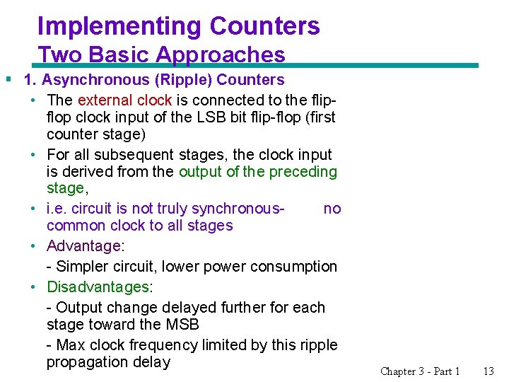
Implementing Counters Two Basic Approaches § 1. Asynchronous (Ripple) Counters • The external clock is connected to the flipflop clock input of the LSB bit flip-flop (first counter stage) • For all subsequent stages, the clock input is derived from the output of the preceding stage, • i. e. circuit is not truly synchronousno common clock to all stages • Advantage: - Simpler circuit, lower power consumption • Disadvantages: - Output change delayed further for each stage toward the MSB - Max clock frequency limited by this ripple propagation delay Chapter 3 - Part 1 13

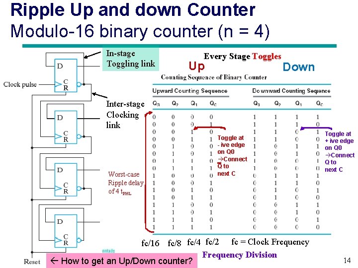
Ripple Up and down Counter Modulo-16 binary counter (n = 4) In-stage Toggling link Every Stage Toggles Up Down Inter-stage Clocking link Worst-case Ripple delay of 4 t. PHL Toggle at - ive edge on Q 0 Connect Q to next C fc/16 fc/8 fc/4 fc/2 fc = Clock Frequency Division How to get an Up/Down counter? Toggle at + ive edge on Q 0 Connect Q to next C 14

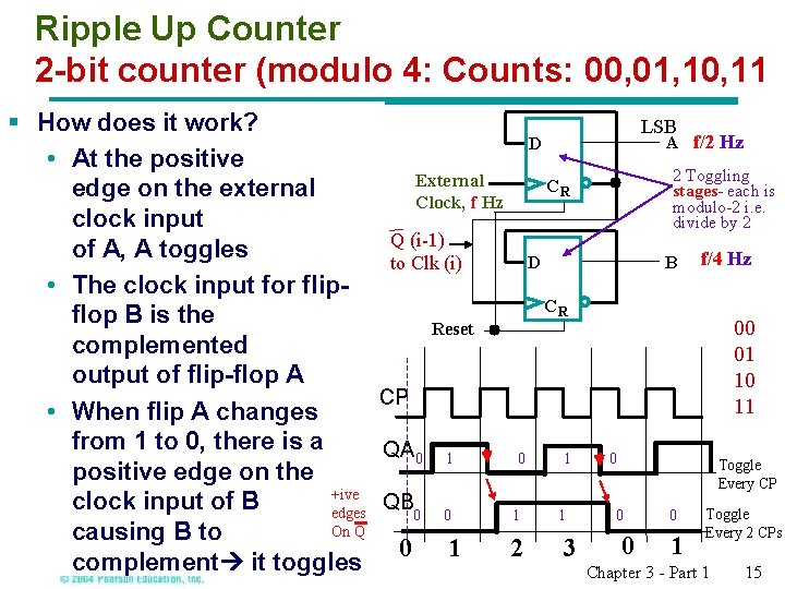
Ripple Up Counter 2 -bit counter (modulo 4: Counts: 00, 01, 10, 11 § How does it work? D • At the positive External CR edge on the external Clock, f Hz clock input Q (i-1) of A, A toggles D to Clk (i) • The clock input for flip. CR flop B is the Reset complemented output of flip-flop A CP • When flip A changes from 1 to 0, there is a QA 0 1 positive edge on the +ive QB clock input of B edges 0 0 1 1 On Q causing B to 0 1 2 3 complement it toggles LSB A f/2 Hz 2 Toggling stages- each is modulo-2 i. e. divide by 2 B f/4 Hz 00 01 10 11 0 Toggle Every CP 0 0 0 1 Toggle Every 2 CPs Chapter 3 - Part 1 15

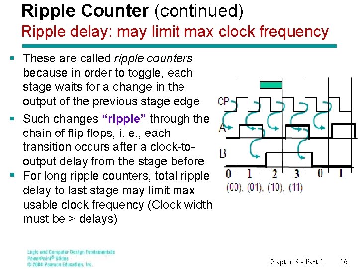
Ripple Counter (continued) Ripple delay: may limit max clock frequency § These are called ripple counters because in order to toggle, each stage waits for a change in the output of the previous stage edge § Such changes “ripple” through the chain of flip-flops, i. e. , each transition occurs after a clock-tooutput delay from the stage before § For long ripple counters, total ripple delay to last stage may limit max usable clock frequency (Clock width must be > delays) Chapter 3 - Part 1 16

Implementing Counters 2 § Synchronous Counters • System clock is connected directly to the clock inputs of ALL flip-flops (truly synchronous) • Combinational logic is used to implement the desired state sequencing as inputs to the D inputs of the flip-flops Chapter 3 - Part 1 17

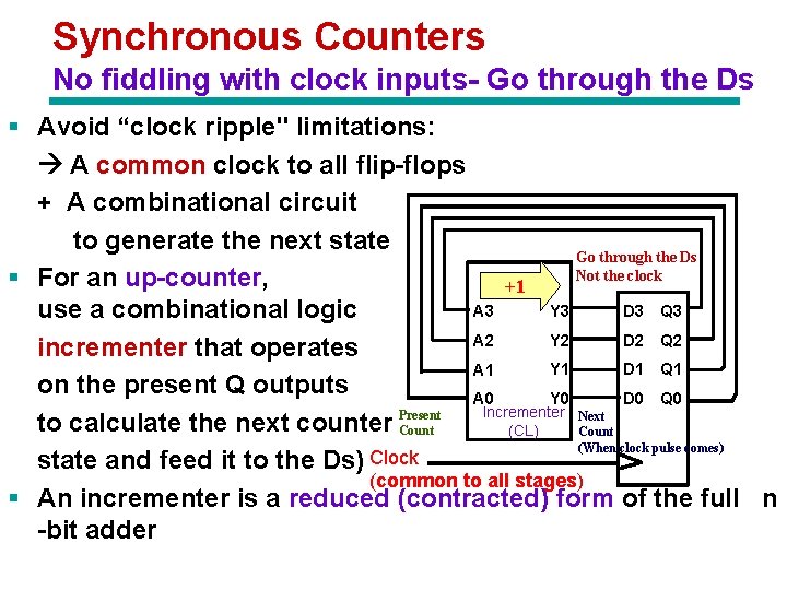
Synchronous Counters No fiddling with clock inputs- Go through the Ds § Avoid “clock ripple" limitations: A common clock to all flip-flops + A combinational circuit to generate the next state Go through the Ds Not the clock § For an up-counter, +1 Y 3 D 3 Q 3 A 3 use a combinational logic Y 2 D 2 Q 2 A 2 incrementer that operates Y 1 D 1 Q 1 A 1 on the present Q outputs Y 0 D 0 Q 0 A 0 Incrementer Next to calculate the next counter Present Count (CL) (When clock pulse comes) Clock state and feed it to the Ds) (common to all stages) § An incrementer is a reduced (contracted) form of the full n -bit adder Chapter 3 - Part 1 18

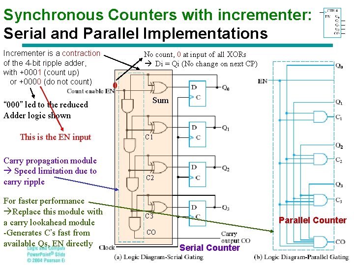
Synchronous Counters with incrementer: Serial and Parallel Implementations Incrementer is a contraction of the 4 -bit ripple adder, with +0001 (count up) or +0000 (do not count) “ 000” led to the reduced Adder logic shown This is the EN input Carry propagation module Speed limitation due to carry ripple For faster performance Replace this module with a carry lookahead module -Generates C’s fast from available Qs, EN directly No count, 0 at input of all XORs Di = Qi (No change on next CP) 0 Sum C 1 C 2 C 3 Parallel Counter CO Serial Counter Chapter 3 - Part 1 19

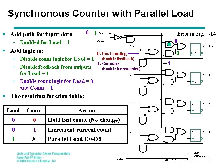
Synchronous Counter with Parallel Load 0 1 Load § Add path for input data • Enabled for Load = 1 Error in Fig. 7 -14 0 Count D 0 § Add logic to: • Disable count logic for Load = 1 • Disable feedback from outputs for Load = 1 • Enable count logic for Load = 0 and Count = 1 0: Not Counting (Enable feedback) 1: Counting (Enable incrementer) D 1 Q 0 D 0 C 1 Q 1 D C § The resulting function table: D 2 Load Count 0 0 Hold last count (No change) 0 1 Increment current count 1 X Parallel Load D 0 -D 3 Q 2 D Action C D 3 Q 3 D C Clock Carry Output CO Chapter 3 - Part 1 20

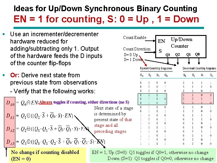
Ideas for Up/Down Synchronous Binary Counting EN = 1 for counting, S: 0 = Up , 1 = Down § Use an incrementer/decrementer hardware reduced for adding/subtracting only 1. Output of the hardware feeds the D inputs of the counter flip-flops Count Enable Count Direction S= 0 Up S= 1 Down Up/Down Counter EN S Q 3 Q 2 Q 1 Q 0 § Or: Derive next state from previous state from observations - Verify that the following works: ; Always toggles if counting, either directions (no S) Next state of a stage is determined by present state of that stage and all preceding stages No change if counting disabled (EN = 0) EN = 1, Up (S=0): Q 1 toggles if Q 0=1, otherwise no change Down (S=1): Q 1 toggles if Q 0=0, otherwise Chapter 3 - Part 1 no change 21

Modulo N (i. e. divide by N) Counters N counting states: 0, 1, 2, …, (N-1) § The following techniques use an n-bit (2 n >= N) binary counter with synchronous clear or parallel load: • Detect terminal count (N – 1) and use to synchronously Clear the counter to 0 (first count) on next clock pulse • Detect terminal count (N – 1) in to synchronously Load in the value 0 (first count) on next clock pulse § Caution: Note that in the cases above, asynchronous Clear or load is problematic, as the terminal count removes itself immediately (not at the next clock cycle) and therefore may not have a chance to exist! § Alternatively, custom design a modulo N counter as a sequential circuit (FSM) Chapter 3 - Part 1 22

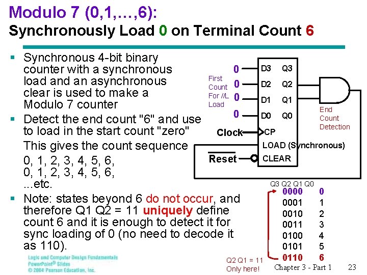
Modulo 7 (0, 1, …, 6): Synchronously Load 0 on Terminal Count 6 § Synchronous 4 -bit binary 0 counter with a synchronous First load an asynchronous Count 0 clear is used to make a For //L 0 Load Modulo 7 counter 0 § Detect the end count "6" and use to load in the start count "zero" Clock This gives the count sequence Reset 0, 1, 2, 3, 4, 5, 6, . . . etc. § Note: states beyond 6 do not occur, and therefore Q 1 Q 2 = 11 uniquely define count 6 and it is enough to detect it for sync loading of 0 (no need to decode it as 110). D 3 Q 3 D 2 Q 2 D 1 Q 1 D 0 Q 0 CP End Count Detection LOAD (Synchronous) CLEAR Q 2 Q 1 = 11 Only here! Q 3 Q 2 Q 1 Q 0 0001 0010 0011 0100 0101 0110 0 1 2 3 4 5 6 Chapter 3 - Part 1 23

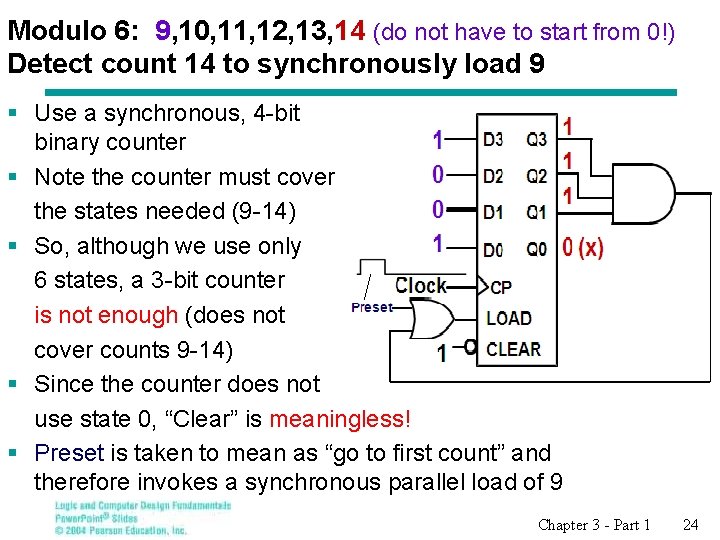
Modulo 6: 9, 10, 11, 12, 13, 14 (do not have to start from 0!) Detect count 14 to synchronously load 9 § Use a synchronous, 4 -bit binary counter § Note the counter must cover the states needed (9 -14) § So, although we use only 6 states, a 3 -bit counter is not enough (does not cover counts 9 -14) § Since the counter does not use state 0, “Clear” is meaningless! § Preset is taken to mean as “go to first count” and therefore invokes a synchronous parallel load of 9 Chapter 3 - Part 1 24

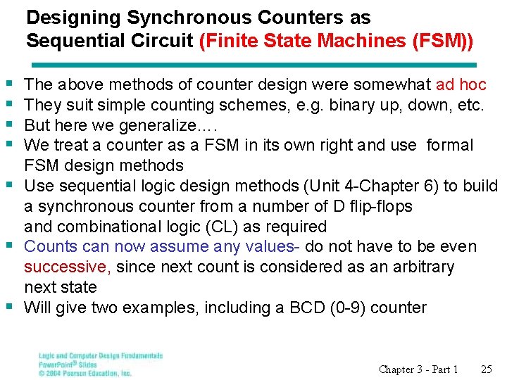
Designing Synchronous Counters as Sequential Circuit (Finite State Machines (FSM)) § § The above methods of counter design were somewhat ad hoc They suit simple counting schemes, e. g. binary up, down, etc. But here we generalize…. We treat a counter as a FSM in its own right and use formal FSM design methods § Use sequential logic design methods (Unit 4 -Chapter 6) to build a synchronous counter from a number of D flip-flops and combinational logic (CL) as required § Counts can now assume any values- do not have to be even successive, since next count is considered as an arbitrary next state § Will give two examples, including a BCD (0 -9) counter Chapter 3 - Part 1 25

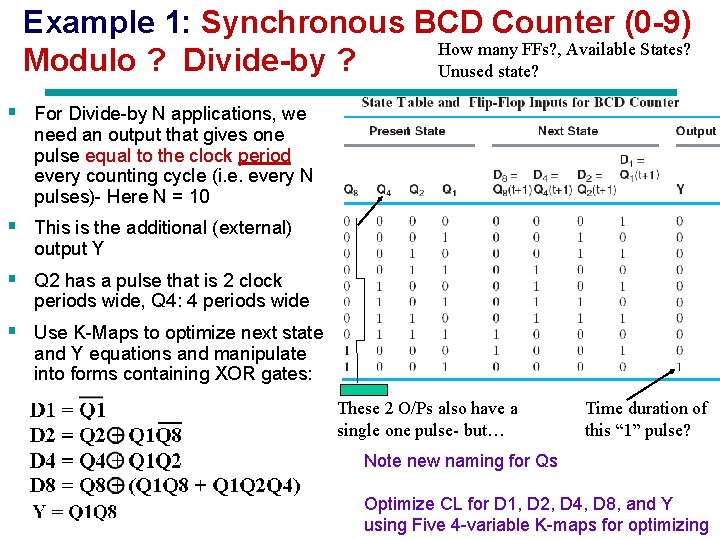
Example 1: Synchronous BCD Counter (0 -9) How many FFs? , Available States? Modulo ? Divide-by ? Unused state? § For Divide-by N applications, we need an output that gives one pulse equal to the clock period every counting cycle (i. e. every N pulses)- Here N = 10 § This is the additional (external) output Y § Q 2 has a pulse that is 2 clock periods wide, Q 4: 4 periods wide § Use K-Maps to optimize next state and Y equations and manipulate into forms containing XOR gates: These 2 O/Ps also have a single one pulse- but… Time duration of this “ 1” pulse? Note new naming for Qs Optimize CL for D 1, D 2, D 4, D 8, and Y Chapter 3 for - Part 1 26 using Five 4 -variable K-maps optimizing

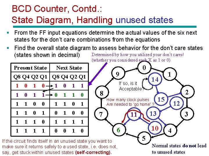
BCD Counter, Contd. : State Diagram, Handling unused states § From the FF input equations determine the actual values of the six next states for the don’t care combinations from the equations § Find the overall state diagram to assess behavior for the don’t care states Determined by how you utilized your don’t cares! (states shown in decimal) (whether you considered each X as 1 or 0) Present State Next State 9 Q 8 Q 4 Q 2 Q 1 1 0 1 0 1 1 0 0 1 1 1 0 1 0 0 1 1 1 0 0 If so, is it Acceptable? 8 14 How many clock pulses Are needed to ‘go home’ ? 7 2 15 12 13 11 10 6 If the circuit finds itself in an unused state you want to make sure it returns safely to a used state, i. e. does not, say, get stuck within unused states (self-correcting). 1 3 4 5 Normal states do not lead - Part 1 27 to. Chapter unused 3 states

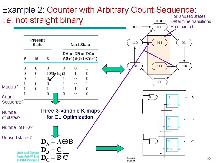
Example 2: Counter with Arbitrary Count Sequence: For Unused states: i. e. not straight binary Determine transitions From circuit Missing? Modulo? Count Sequence? Number of states? Three 3 -variable K-maps for CL Optimization Number of FFs? Unused states? Chapter 3 - Part 1 28