Lecture 31 FlipFlops Clocks Timing Last lecture Finite


- Slides: 35

Lecture #31 Flip-Flops, Clocks, Timing • Last lecture: – Finite State Machines • This lecture: – Digital circuits with feedback – Clocks – Flip-Flops 11/12/2004 EE 42 fall 2004 lecture 31 1

Clocked Logic • In the last few lectures, we have been discussing the implementation of circuits which can break a problem down into a sequence of events, as contrasted with evaluation of a single Boolean expression (Combinatorial Logic) 11/12/2004 EE 42 fall 2004 lecture 31 2

Definition: Combinatorial logic is a set of digital gates which produces an output based solely on its current inputs. A combinatorial logic circuit can be described using a truth table 11/12/2004 EE 42 fall 2004 lecture 31 3

Definition: Truth table • A Truth table is a description of a digital circuit which is a tabulation of all possible inputs, and the outputs which will result from those inputs. • Two combinatorial logic circuits are considered logically equivalent if they have the same truth table 11/12/2004 EE 42 fall 2004 lecture 31 4

Sequential Logic • In order to solve more complex problems using a sequence of steps, we looked at the concept of feedback of the output of intermediate results back into the circuit for additional processing. In solving the problems caused by this, we arrived at the finite state machine with latched and clocked feedback. 11/12/2004 EE 42 fall 2004 lecture 31 5

• In the next two lectures, we will discuss the implementation of sequential logic, latches, clocks, and the various problems which can occur in dynamic digital logic circuits. 11/12/2004 EE 42 fall 2004 lecture 31 6

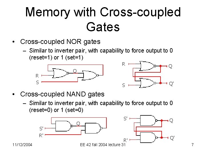
Memory with Cross-coupled Gates • Cross-coupled NOR gates – Similar to inverter pair, with capability to force output to 0 (reset=1) or 1 (set=1) R Q S Q' Q R S • Cross-coupled NAND gates – Similar to inverter pair, with capability to force output to 0 (reset=0) or 1 (set=0) S' R' 11/12/2004 Q S' R' EE 42 fall 2004 lecture 31 Q Q' 7

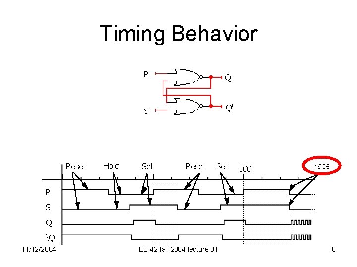
Timing Behavior Reset Hold R Q S Q' Set Reset Set 100 Race R S Q Q 11/12/2004 EE 42 fall 2004 lecture 31 8

Race condition on falling edge of S/R • If both set and reset are high, then the value latched will be whichever falling edge happens last. If this is controlled by delays in the logic, then the outcome of which is first might be random, erratic, or dependent on other parameters. 11/12/2004 EE 42 fall 2004 lecture 31 9

Definition: Race, or Race condition • A Race condition is when a device's output depends on two [or more] nearly simultaneous events to occur, and where which signal arrives first will change the output of the circuit. If the race condition is so close in time, the output may be unpredictable. When the circuit is manufactured, slight differences can cause a change in the operation of the circuit. A race condition can be a logic hazard, or can result in a random value being held in a latch. 11/12/2004 EE 42 fall 2004 lecture 31 10

Definition: Glitch, Hazard • A Glitch is a momentary output of a digital circuit of an incorrect value • A Static Hazard is when a single variable change at the input causes a momentary change in the output. • A Dynamic Hazard occurs when a change in the input causes multiple changes in the output. Latches can remove glitches by allowing the output to progress only after the logic has had adequate time to stabilize on the correct output. It is desirable to design out hazard in the logic, because the extra transitions consume power and produce excess noise. If Static Hazards are removed from the design, Dynamic Hazards will not occur. If not removed by latches or Flip-Flops, timing hazards will develop as random or intermittent circuit failures. 11/12/2004 EE 42 fall 2004 lecture 31 11

Definition: Latch • A latch is a digital circuit which will hold a value when the level of a latching signal is at a certain level. For example, while the reset signal is low, the SR latch will hold the value of Q, (and set it if Set goes high). The alternative is to set the output only at an rising or falling edge, which is referred to as being edge triggered. 11/12/2004 EE 42 fall 2004 lecture 31 12

Level Trigger • A level trigger refers to the capture of a value while a signal (clock, for example, is high (or low). The data must be held valid and stable during the entire time it is being sampled Data Clock 11/12/2004 EE 42 fall 2004 lecture 31 13

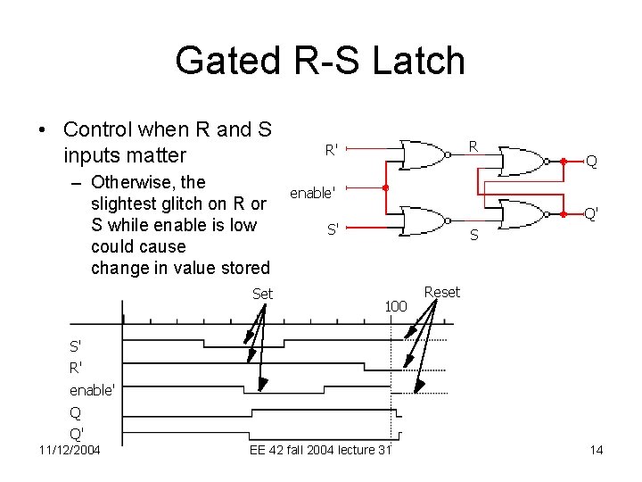
Gated R-S Latch • Control when R and S inputs matter – Otherwise, the slightest glitch on R or S while enable is low could cause change in value stored Set R R' Q enable' Q' S' S 100 Reset S' R' enable' Q Q' 11/12/2004 EE 42 fall 2004 lecture 31 14

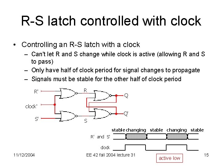
R-S latch controlled with clock • Controlling an R-S latch with a clock – Can't let R and S change while clock is active (allowing R and S to pass) – Only have half of clock period for signal changes to propagate – Signals must be stable for the other half of clock period R' R Q clock' S' Q' S stable changing stable R' and S' clock 11/12/2004 EE 42 fall 2004 lecture 31 active low 15

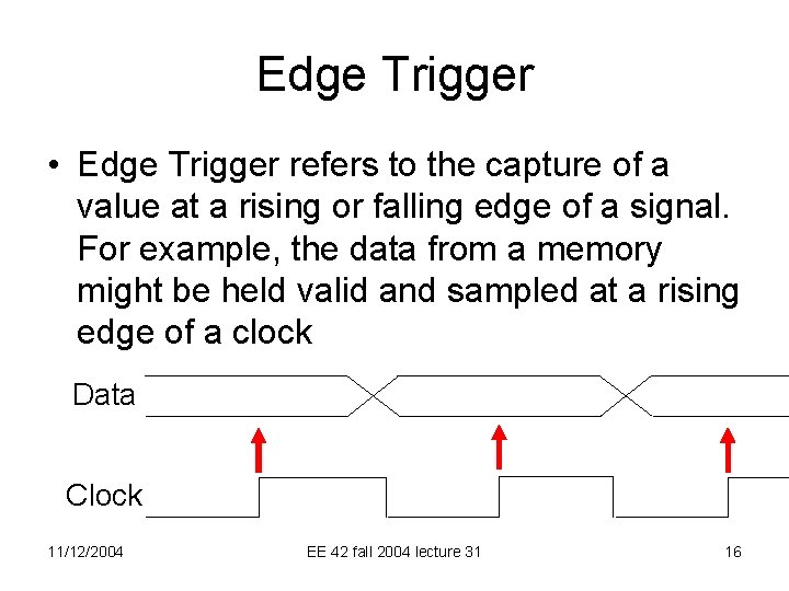
Edge Trigger • Edge Trigger refers to the capture of a value at a rising or falling edge of a signal. For example, the data from a memory might be held valid and sampled at a rising edge of a clock Data Clock 11/12/2004 EE 42 fall 2004 lecture 31 16

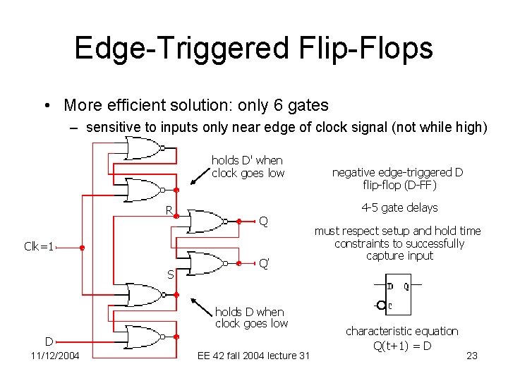
Definition: Flip-Flop • A flip flop is a digital circuit which will capture a value at a rising (or falling) edge, and will hold that value. It will only change the value held at an edge, and will not pass on transitions from the inputs while the clock or latch signal is either high or low. 11/12/2004 EE 42 fall 2004 lecture 31 17

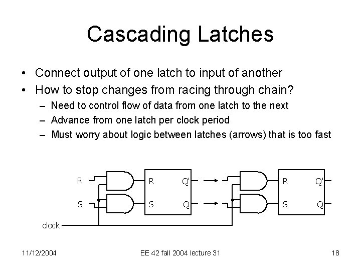
Cascading Latches • Connect output of one latch to input of another • How to stop changes from racing through chain? – Need to control flow of data from one latch to the next – Advance from one latch per clock period – Must worry about logic between latches (arrows) that is too fast R R Q' S S Q clock 11/12/2004 EE 42 fall 2004 lecture 31 18

Master-Slave Structure • Break flow by alternating clocks (like an air-lock) – Use positive clock to latch inputs into one R-S latch – Use negative clock to change outputs with another R-S latch • View pair as one basic unit – master-slave flip-flop – twice as much logic – output changes a few gate delays after the falling edge of clock but does not affect any cascaded flip-flops slave stage master stage R R Q' S S Q P' P R Q' S Q CLK 11/12/2004 EE 42 fall 2004 lecture 31 19

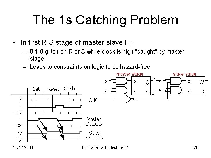
The 1 s Catching Problem • In first R-S stage of master-slave FF – 0 -1 -0 glitch on R or S while clock is high "caught" by master stage – Leads to constraints on logic to be hazard-free slave stage master stage Set S R CLK P P' Q Q' 11/12/2004 1 s Reset catch R R Q' S S Q P' P R Q' S Q CLK Master Outputs Slave Outputs EE 42 fall 2004 lecture 31 20

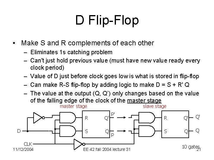
D Flip-Flop • Make S and R complements of each other – Eliminates 1 s catching problem – Can't just hold previous value (must have new value ready every clock period) – Value of D just before clock goes low is what is stored in flip-flop – Can make R-S flip-flop by adding logic to make D = S + R' Q – The value at the output (Q, Q’) only changes based on the value of the falling edge of the clock of the master stage slave stage master stage D R Q' S Q P' P CLK 11/12/2004 EE 42 fall 2004 lecture 31 R Q' Q' S Q Q 10 gates 21

Edge triggering • The proceeding slide showed how a flip flop could be designed by using two latches which are cascaded in a masterslave relationship. • Another way of creating an edge triggered flip flop is to use logic with feedback, as in the following slide. 11/12/2004 EE 42 fall 2004 lecture 31 22

Edge-Triggered Flip-Flops • More efficient solution: only 6 gates – sensitive to inputs only near edge of clock signal (not while high) holds D' when clock goes low R Q Clk=1 S Q’ holds D when clock goes low D 11/12/2004 EE 42 fall 2004 lecture 31 negative edge-triggered D flip-flop (D-FF) 4 -5 gate delays must respect setup and hold time constraints to successfully capture input characteristic equation Q(t+1) = D 23

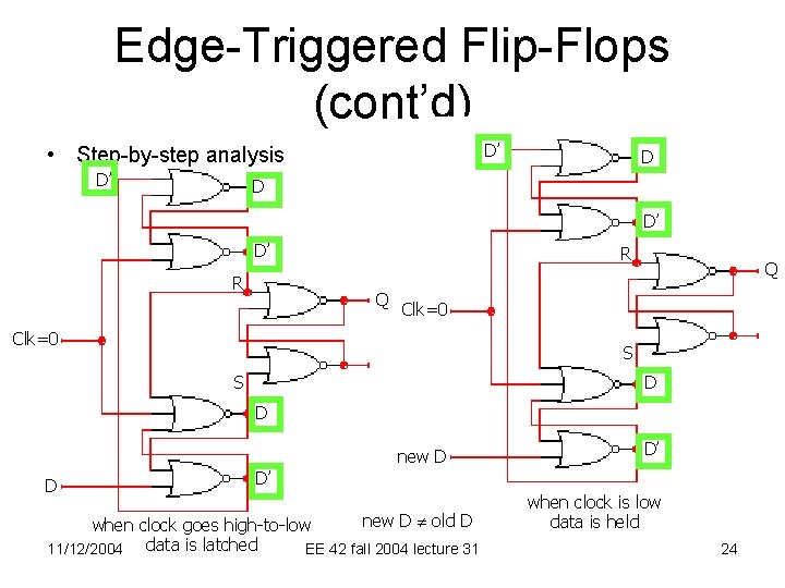
Edge-Triggered Flip-Flops (cont’d) D’ • Step-by-step analysis D’ D D D’ D’ R R Q Q Clk=0 S S D D new D D D’ D’ new D old D when clock goes high-to-low 11/12/2004 data is latched EE 42 fall 2004 lecture 31 when clock is low data is held 24

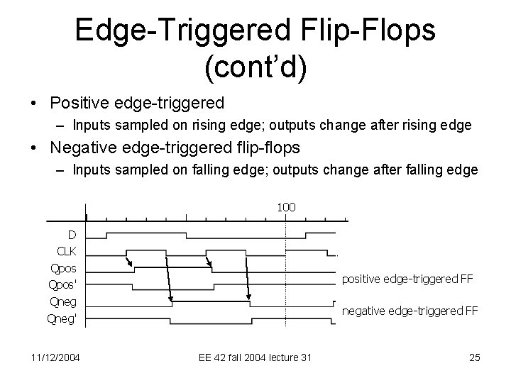
Edge-Triggered Flip-Flops (cont’d) • Positive edge-triggered – Inputs sampled on rising edge; outputs change after rising edge • Negative edge-triggered flip-flops – Inputs sampled on falling edge; outputs change after falling edge 100 D CLK Qpos' Qneg' 11/12/2004 positive edge-triggered FF negative edge-triggered FF EE 42 fall 2004 lecture 31 25

Timing Methodologies • Rules for interconnecting components and clocks – Guarantee properation of system when strictly followed • Approach depends on building blocks used for memory elements – Focus on systems with edge-triggered flip-flops • Found in programmable logic devices – Many custom integrated circuits focus on level-sensitive latches • Basic rules for correct timing: – (1) Correct inputs, with respect to time, are provided to the flip-flops – (2) No flip-flop changes state more than once per clocking event 11/12/2004 EE 42 fall 2004 lecture 31 26

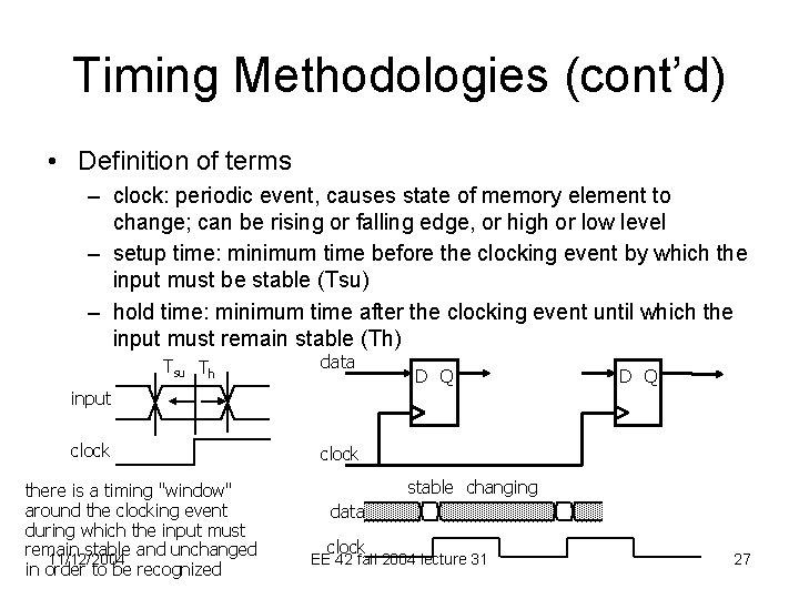
Timing Methodologies (cont’d) • Definition of terms – clock: periodic event, causes state of memory element to change; can be rising or falling edge, or high or low level – setup time: minimum time before the clocking event by which the input must be stable (Tsu) – hold time: minimum time after the clocking event until which the input must remain stable (Th) Tsu Th data D Q input clock there is a timing "window" around the clocking event during which the input must remain stable and unchanged 11/12/2004 in order to be recognized clock stable changing data clock EE 42 fall 2004 lecture 31 27

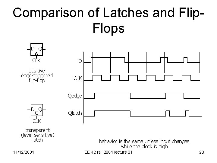
Comparison of Latches and Flip. Flops D Q CLK positive edge-triggered flip-flop D CLK Qedge D Q G Qlatch CLK transparent (level-sensitive) latch 11/12/2004 behavior is the same unless input changes while the clock is high EE 42 fall 2004 lecture 31 28

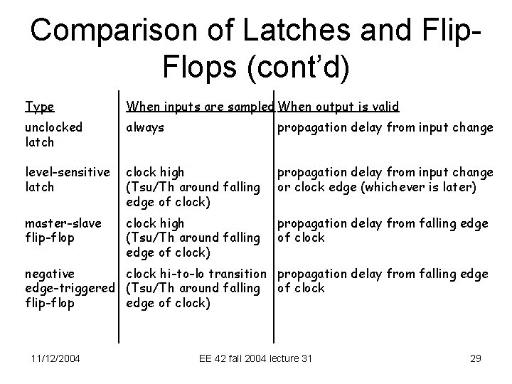
Comparison of Latches and Flip. Flops (cont’d) Type When inputs are sampled When output is valid unclocked latch always propagation delay from input change level-sensitive latch clock high (Tsu/Th around falling edge of clock) propagation delay from input change or clock edge (whichever is later) master-slave flip-flop clock high (Tsu/Th around falling edge of clock) propagation delay from falling edge of clock negative clock hi-to-lo transition propagation delay from falling edge-triggered (Tsu/Th around falling of clock flip-flop edge of clock) 11/12/2004 EE 42 fall 2004 lecture 31 29

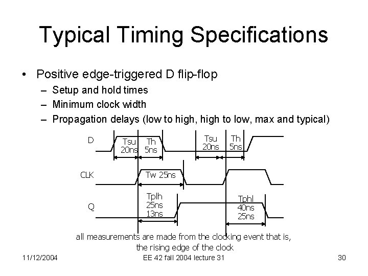
Typical Timing Specifications • Positive edge-triggered D flip-flop – Setup and hold times – Minimum clock width – Propagation delays (low to high, high to low, max and typical) D CLK Q Tsu Th 20 ns 5 ns Tsu 20 ns Th 5 ns Tw 25 ns Tplh 25 ns 13 ns Tphl 40 ns 25 ns all measurements are made from the clocking event that is, the rising edge of the clock 11/12/2004 EE 42 fall 2004 lecture 31 30

Definition: Metastability • Metastability is a condition in which a latch or a Flip-Flop is exactly balanced between the logic high and logic low states. This can be caused by an asynchronous data signal input to a clocked Flip Flop. The resulting output may stay undefined for some time. 11/12/2004 EE 42 fall 2004 lecture 31 31

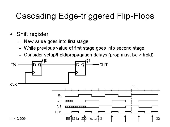
Cascading Edge-triggered Flip-Flops • Shift register – New value goes into first stage – While previous value of first stage goes into second stage – Consider setup/hold/propagation delays (prop must be > hold) IN D Q Q 0 D Q Q 1 OUT CLK 100 IN Q 0 Q 1 CLK 11/12/2004 EE 42 fall 2004 lecture 31 32

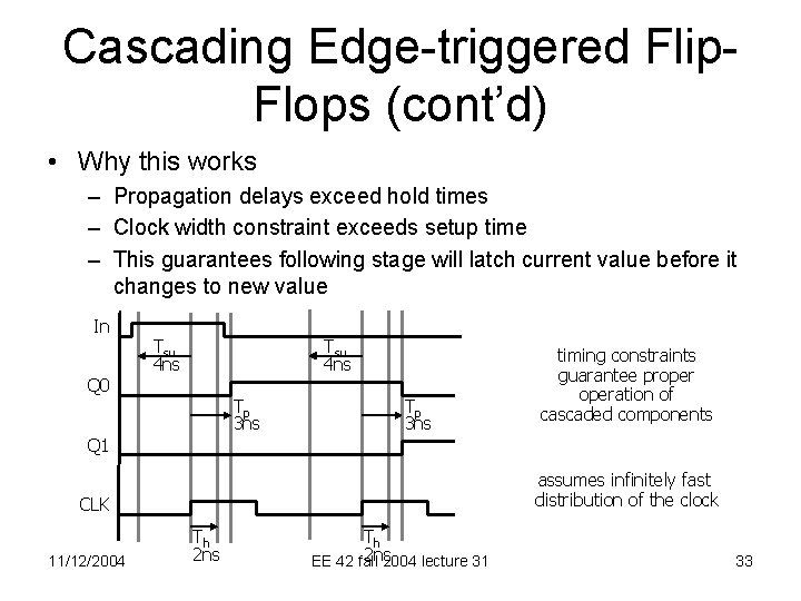
Cascading Edge-triggered Flip. Flops (cont’d) • Why this works – Propagation delays exceed hold times – Clock width constraint exceeds setup time – This guarantees following stage will latch current value before it changes to new value In Tsu 4 ns Q 0 Tp 3 ns timing constraints guarantee properation of cascaded components Q 1 assumes infinitely fast distribution of the clock CLK 11/12/2004 Th 2 ns EE 42 fall 2004 lecture 31 33

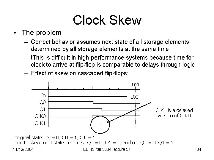
Clock Skew • The problem – Correct behavior assumes next state of all storage elements determined by all storage elements at the same time – t. This is difficult in high-performance systems because time for clock to arrive at flip-flop is comparable to delays through logic – Effect of skew on cascaded flip-flops: In Q 0 Q 1 CLK 0 CLK 1 100 CLK 1 is a delayed version of CLK 0 original state: IN = 0, Q 0 = 1, Q 1 = 1 due to skew, next state becomes: Q 0 = 0, Q 1 = 0, and not Q 0 = 0, Q 1 = 1 11/12/2004 EE 42 fall 2004 lecture 31 34

Summary of Latches and Flip. Flops • Development of D-Flip-Flop – Level-sensitive used in custom integrated circuits • can be made with 4 switches – Edge-triggered used in programmable logic devices – Good choice for data storage register • Historically J-K Flip Flop was popular but now never used – Similar to R-S but with 1 -1 being used to toggle output (complement state) – Can always be implemented using D-FF • Preset and clear inputs are highly desirable on flip-flops – Used at start-up or to reset system to a known state 11/12/2004 EE 42 fall 2004 lecture 31 35