Sequential Sytems Part 2 Registers Counters Shift Registers

- Slides: 37

Sequential Sytems. Part 2. Registers. Counters. Shift Registers. (Lab. 4, 5) IAX 0600 Digital Systems Design Alexander Sudnitson Tallinn University of Technology 1

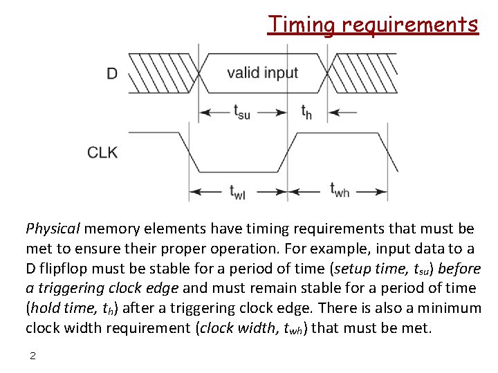
Timing requirements Physical memory elements have timing requirements that must be met to ensure their properation. For example, input data to a D flipflop must be stable for a period of time (setup time, tsu) before a triggering clock edge and must remain stable for a period of time (hold time, th) after a triggering clock edge. There is also a minimum clock width requirement (clock width, twh) that must be met. 2

Metastable event Violating Setup Time or Hold Time Requirements One result of not meeting setup time or hold time requirements is the possibility of a metastable event. The term metastable event denotes the situation where a flipflop’s output either remains between valid states for an unusually long period of time or fails to complete the transition to the desired state after a triggering clock edge. Metastable events can result in incorrect system operation. 3

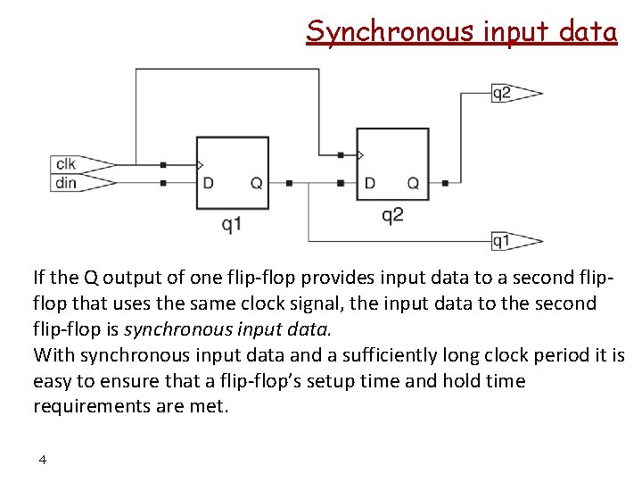
Synchronous input data If the Q output of one flip-flop provides input data to a second flipflop that uses the same clock signal, the input data to the second flip-flop is synchronous input data. With synchronous input data and a sufficiently long clock period it is easy to ensure that a flip-flop’s setup time and hold time requirements are met. 4

Use of flip-flops versus latches Generally, the use of latches as simple storage elements is not recommended. Traditionally, latches had the advantage in custom IC design of requiring fewer transistors, thus requiring half as much IC area. However, latches in FPGAs are typically implemented using memory elements that can be configured as either a latch or flipflop. The amount of chip area taken by a configurable memory element in a FPGA is fixed, regardless of whether it is configured as a latch or flip-flop. More importantly, use of latches increases the timing complexity of a design. This necessitates much more careful design techniques and timing analysis to ensure correct operation. 5

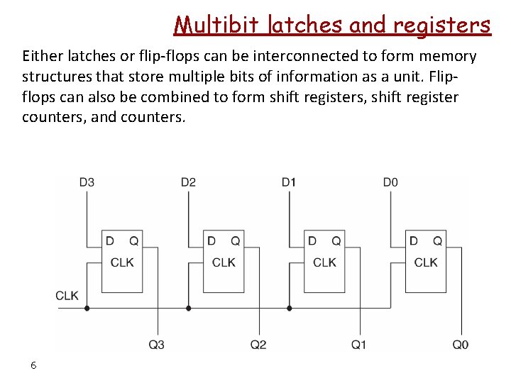
Multibit latches and registers Either latches or flip-flops can be interconnected to form memory structures that store multiple bits of information as a unit. Flipflops can also be combined to form shift registers, shift register counters, and counters. 6

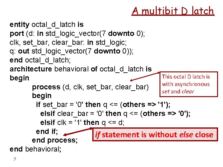
A multibit D latch entity octal_d_latch is port (d: in std_logic_vector(7 downto 0); clk, set_bar, clear_bar: in std_logic; q: out std_logic_vector(7 downto 0)); end octal_d_latch; architecture behavioral of octal_d_latch is This octal D latch is begin with asynchronous process (d, clk, set_bar, clear_bar) set and clear begin if set_bar = '0' then q <= (others => '1'); elsif clear_bar = '0' then q <= (others => '0'); elsif clk = '1' then q <= d; end if; if statement is without else close end process; end behavioral; 7

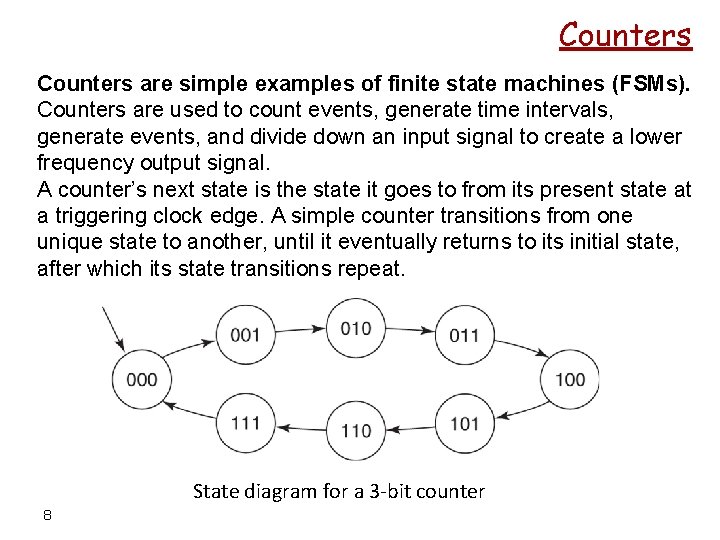
Counters are simple examples of finite state machines (FSMs). Counters are used to count events, generate time intervals, generate events, and divide down an input signal to create a lower frequency output signal. A counter’s next state is the state it goes to from its present state at a triggering clock edge. A simple counter transitions from one unique state to another, until it eventually returns to its initial state, after which its state transitions repeat. State diagram for a 3 -bit counter 8

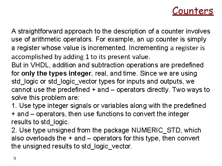
Counters A straightforward approach to the description of a counter involves use of arithmetic operators. For example, an up counter is simply a register whose value is incremented. Incrementing a register is accomplished by adding 1 to its present value. But in VHDL, addition and subtraction operations are predefined for only the types integer, real, and time. Since we are using std_logic or std_logic_vector types for inputs and outputs, we cannot use the predefined + and – operators directly. Two ways to solve this problem are: 1. Use type integer signals or variables along with the predefined + and – operators, then use functions to convert the integer results to std_logic. 2. Use type unsigned from the package NUMERIC_STD, which also overloads the + and – operators for this type, then convert the unsigned results to std_logic_vector. 9

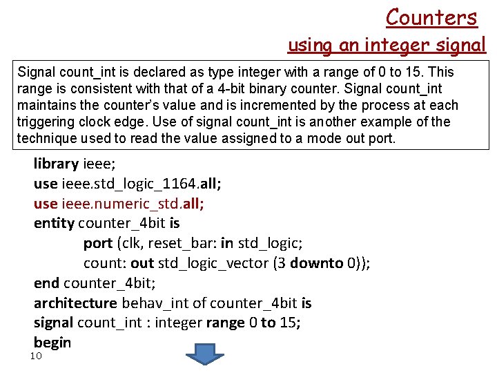
Counters using an integer signal Signal count_int is declared as type integer with a range of 0 to 15. This range is consistent with that of a 4 -bit binary counter. Signal count_int maintains the counter’s value and is incremented by the process at each triggering clock edge. Use of signal count_int is another example of the technique used to read the value assigned to a mode out port. library ieee; use ieee. std_logic_1164. all; use ieee. numeric_std. all; entity counter_4 bit is port (clk, reset_bar: in std_logic; count: out std_logic_vector (3 downto 0)); end counter_4 bit; architecture behav_int of counter_4 bit is signal count_int : integer range 0 to 15; begin 10

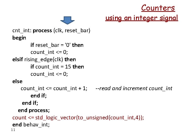
Counters using an integer signal cnt_int: process (clk, reset_bar) begin if reset_bar = '0' then count_int <= 0; elsif rising_edge(clk) then if count_int = 15 then count_int <= 0; else count_int <= count_int + 1; --read and increment count_int end if; end process; count <= std_logic_vector(to_unsigned(count_int, 4)); end behav_int; 11

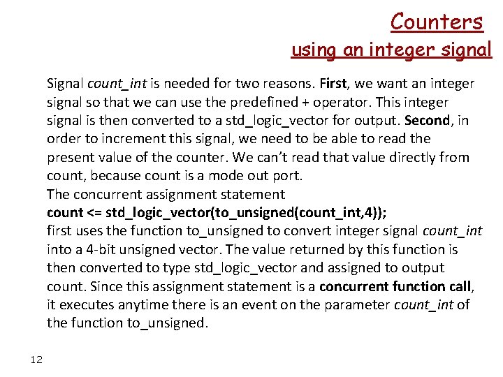
Counters using an integer signal Signal count_int is needed for two reasons. First, we want an integer signal so that we can use the predefined + operator. This integer signal is then converted to a std_logic_vector for output. Second, in order to increment this signal, we need to be able to read the present value of the counter. We can’t read that value directly from count, because count is a mode out port. The concurrent assignment statement count <= std_logic_vector(to_unsigned(count_int, 4)); first uses the function to_unsigned to convert integer signal count_int into a 4 -bit unsigned vector. The value returned by this function is then converted to type std_logic_vector and assigned to output count. Since this assignment statement is a concurrent function call, it executes anytime there is an event on the parameter count_int of the function to_unsigned. 12

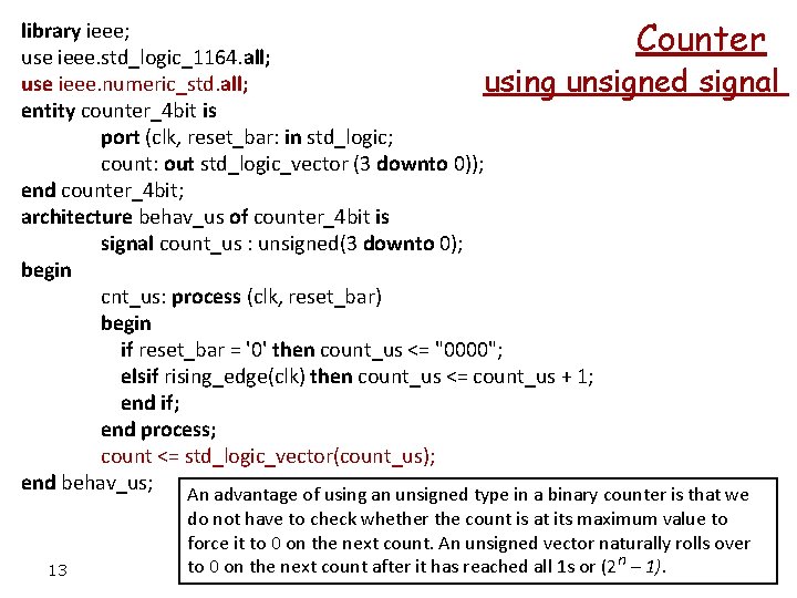
Counter library ieee; use ieee. std_logic_1164. all; use ieee. numeric_std. all; using unsigned entity counter_4 bit is port (clk, reset_bar: in std_logic; count: out std_logic_vector (3 downto 0)); end counter_4 bit; architecture behav_us of counter_4 bit is signal count_us : unsigned(3 downto 0); begin cnt_us: process (clk, reset_bar) begin if reset_bar = '0' then count_us <= "0000"; elsif rising_edge(clk) then count_us <= count_us + 1; end if; end process; count <= std_logic_vector(count_us); end behav_us; 13 signal An advantage of using an unsigned type in a binary counter is that we do not have to check whether the count is at its maximum value to force it to 0 on the next count. An unsigned vector naturally rolls over to 0 on the next count after it has reached all 1 s or (2 n – 1).

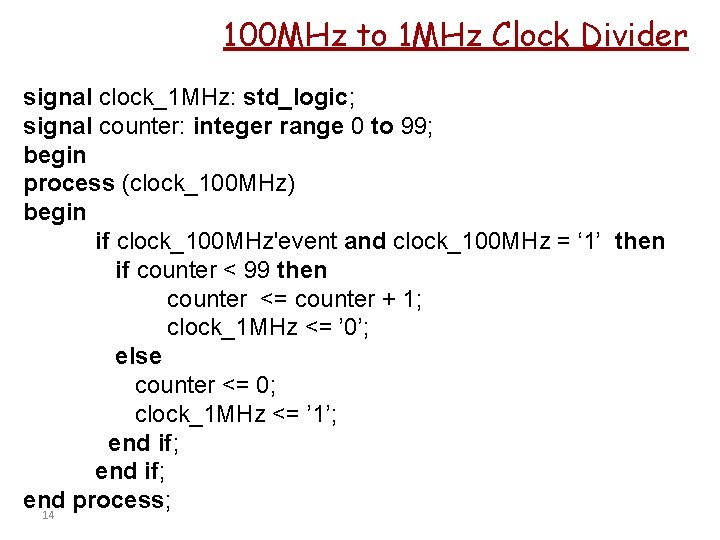
100 MHz to 1 MHz Clock Divider signal clock_1 MHz: std_logic; signal counter: integer range 0 to 99; begin process (clock_100 MHz) begin if clock_100 MHz'event and clock_100 MHz = ‘ 1’ then if counter < 99 then counter <= counter + 1; clock_1 MHz <= ’ 0’; else counter <= 0; clock_1 MHz <= ’ 1’; end if; end process; 14

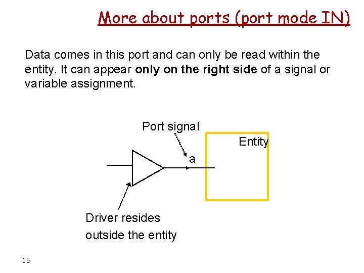
More about ports (port mode IN) Data comes in this port and can only be read within the entity. It can appear only on the right side of a signal or variable assignment. Port signal Entity a Driver resides outside the entity 15

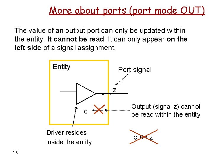
More about ports (port mode OUT) The value of an output port can only be updated within the entity. It cannot be read. It can only appear on the left side of a signal assignment. Entity Port signal z c Driver resides inside the entity 16 Output (signal z) cannot be read within the entity c <= z

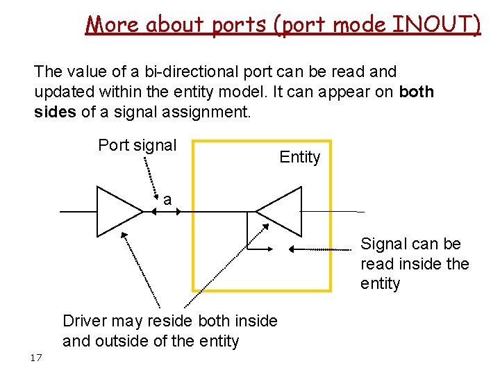
More about ports (port mode INOUT) The value of a bi-directional port can be read and updated within the entity model. It can appear on both sides of a signal assignment. Port signal Entity a Signal can be read inside the entity Driver may reside both inside and outside of the entity 17

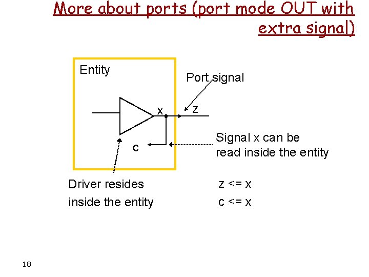
More about ports (port mode OUT with extra signal) Entity Port signal x c Driver resides inside the entity 18 z Signal x can be read inside the entity z <= x c <= x

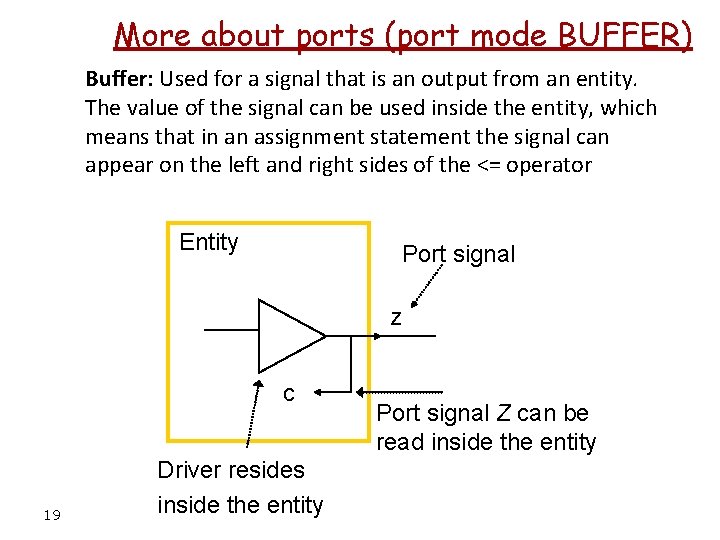
More about ports (port mode BUFFER) Buffer: Used for a signal that is an output from an entity. The value of the signal can be used inside the entity, which means that in an assignment statement the signal can appear on the left and right sides of the <= operator Entity Port signal z c 19 Driver resides inside the entity Port signal Z can be read inside the entity

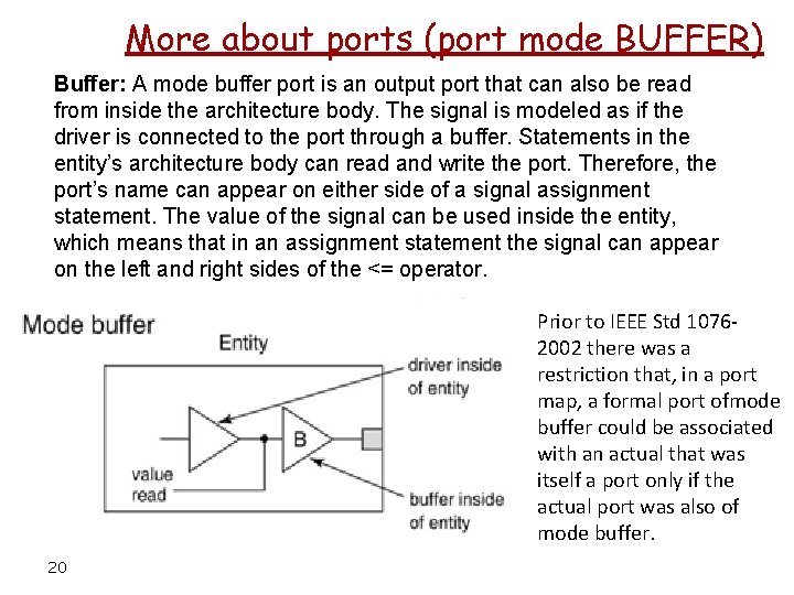
More about ports (port mode BUFFER) Buffer: A mode buffer port is an output port that can also be read from inside the architecture body. The signal is modeled as if the driver is connected to the port through a buffer. Statements in the entity’s architecture body can read and write the port. Therefore, the port’s name can appear on either side of a signal assignment statement. The value of the signal can be used inside the entity, which means that in an assignment statement the signal can appear on the left and right sides of the <= operator. Prior to IEEE Std 10762002 there was a restriction that, in a port map, a formal port ofmode buffer could be associated with an actual that was itself a port only if the actual port was also of mode buffer. 20

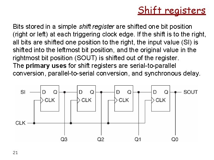
Shift registers Bits stored in a simple shift register are shifted one bit position (right or left) at each triggering clock edge. If the shift is to the right, all bits are shifted one position to the right, the input value (SI) is shifted into the leftmost bit position, and the original value in the rightmost bit position (SOUT) is shifted out of the register. The primary uses for shift registers are serial-to-parallel conversion, parallel-to-serial conversion, and synchronous delay. 21

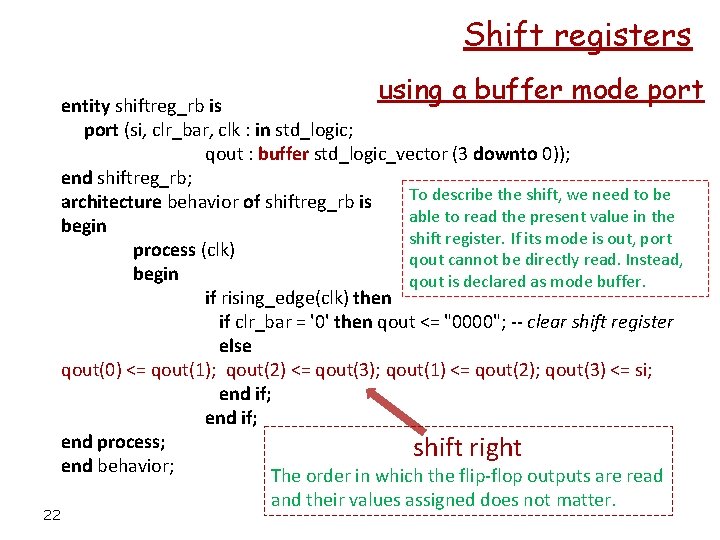
Shift registers using a buffer mode port entity shiftreg_rb is port (si, clr_bar, clk : in std_logic; qout : buffer std_logic_vector (3 downto 0)); end shiftreg_rb; To describe the shift, we need to be architecture behavior of shiftreg_rb is able to read the present value in the begin shift register. If its mode is out, port process (clk) qout cannot be directly read. Instead, begin qout is declared as mode buffer. if rising_edge(clk) then if clr_bar = '0' then qout <= "0000"; -- clear shift register else qout(0) <= qout(1); qout(2) <= qout(3); qout(1) <= qout(2); qout(3) <= si; end if; end process; shift right end behavior; The order in which the flip-flop outputs are read 22 and their values assigned does not matter.

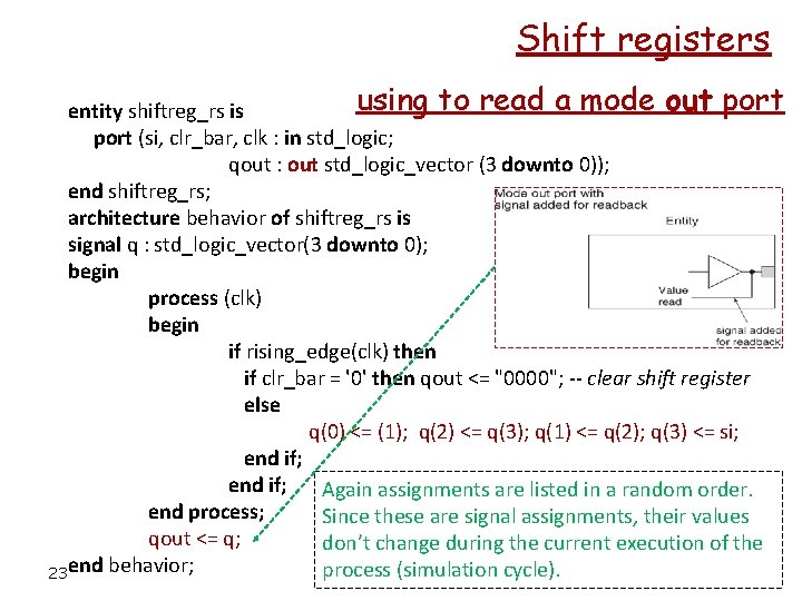
Shift registers using to read a mode out port entity shiftreg_rs is port (si, clr_bar, clk : in std_logic; qout : out std_logic_vector (3 downto 0)); end shiftreg_rs; architecture behavior of shiftreg_rs is signal q : std_logic_vector(3 downto 0); begin process (clk) begin if rising_edge(clk) then if clr_bar = '0' then qout <= "0000"; -- clear shift register else q(0) <= (1); q(2) <= q(3); q(1) <= q(2); q(3) <= si; end if; Again assignments are listed in a random order. end process; Since these are signal assignments, their values qout <= q; don’t change during the current execution of the process (simulation cycle). 23 end behavior;

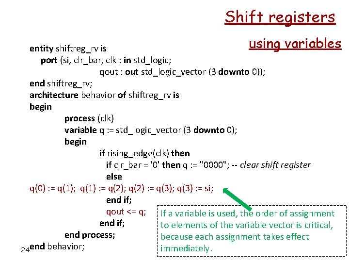
Shift registers using variables entity shiftreg_rv is port (si, clr_bar, clk : in std_logic; qout : out std_logic_vector (3 downto 0)); end shiftreg_rv; architecture behavior of shiftreg_rv is begin process (clk) variable q : = std_logic_vector (3 downto 0); begin if rising_edge(clk) then if clr_bar = '0' then q : = "0000"; -- clear shift register else q(0) : = q(1); q(1) : = q(2); q(2) : = q(3); q(3) : = si; end if; qout <= q; If a variable is used, the order of assignment end if; to elements of the variable vector is critical, end process; because each assignment takes effect immediately. 24 end behavior;

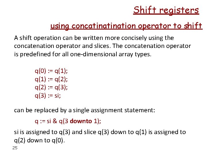
Shift registers using concatination operator to shift A shift operation can be written more concisely using the concatenation operator and slices. The concatenation operator is predefined for all one-dimensional array types. q(0) : = q(1); q(1) : = q(2); q(2) : = q(3); q(3) : = si; can be replaced by a single assignment statement: q : = si & q(3 downto 1); si is assigned to q(3) and slice q(3) down to q(1) is assigned to q(2) down to q(0). 25

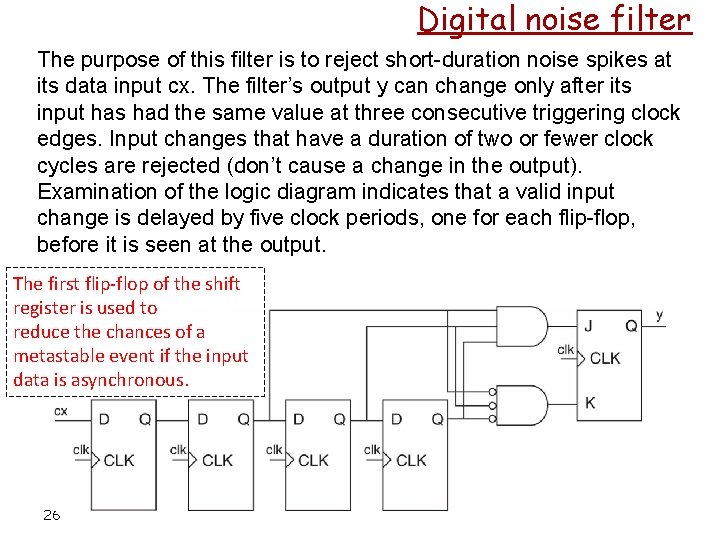
Digital noise filter The purpose of this filter is to reject short-duration noise spikes at its data input cx. The filter’s output y can change only after its input has had the same value at three consecutive triggering clock edges. Input changes that have a duration of two or fewer clock cycles are rejected (don’t cause a change in the output). Examination of the logic diagram indicates that a valid input change is delayed by five clock periods, one for each flip-flop, before it is seen at the output. The first flip-flop of the shift register is used to reduce the chances of a metastable event if the input data is asynchronous. 26

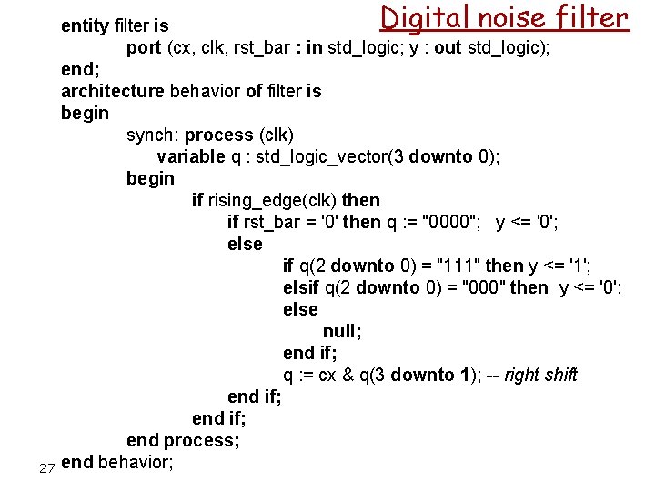
Digital noise filter 27 entity filter is port (cx, clk, rst_bar : in std_logic; y : out std_logic); end; architecture behavior of filter is begin synch: process (clk) variable q : std_logic_vector(3 downto 0); begin if rising_edge(clk) then if rst_bar = '0' then q : = "0000"; y <= '0'; else if q(2 downto 0) = "111" then y <= '1'; elsif q(2 downto 0) = "000" then y <= '0'; else null; end if; q : = cx & q(3 downto 1); -- right shift end if; end process; end behavior;

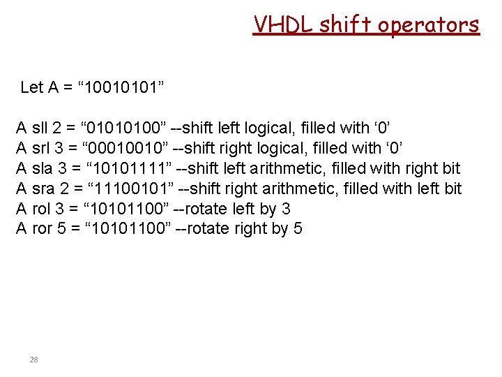
VHDL shift operators Let A = “ 10010101” A sll 2 = “ 01010100” --shift left logical, filled with ‘ 0’ A srl 3 = “ 00010010” --shift right logical, filled with ‘ 0’ A sla 3 = “ 10101111” --shift left arithmetic, filled with right bit A sra 2 = “ 11100101” --shift right arithmetic, filled with left bit A rol 3 = “ 10101100” --rotate left by 3 A ror 5 = “ 10101100” --rotate right by 5 28

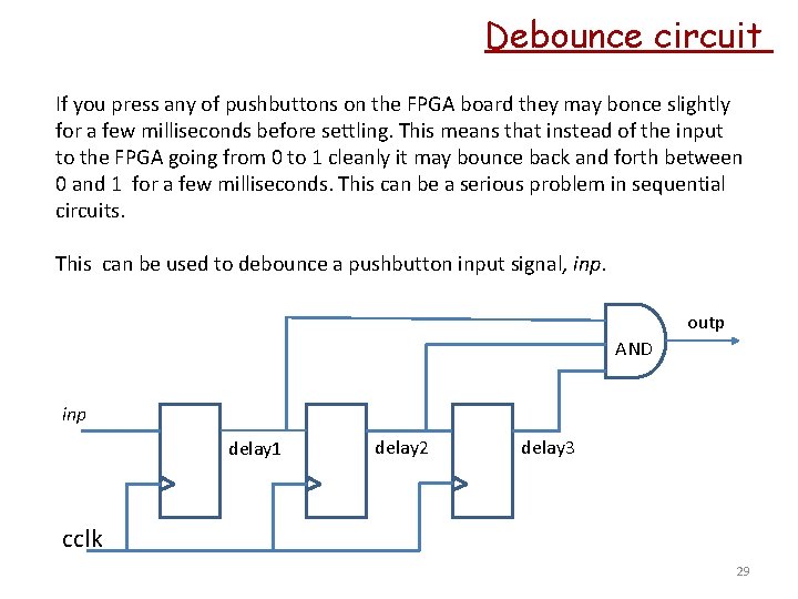
Debounce circuit If you press any of pushbuttons on the FPGA board they may bonce slightly for a few milliseconds before settling. This means that instead of the input to the FPGA going from 0 to 1 cleanly it may bounce back and forth between 0 and 1 for a few milliseconds. This can be a serious problem in sequential circuits. This can be used to debounce a pushbutton input signal, inp. outp AND inp delay 1 delay 2 delay 3 cclk 29

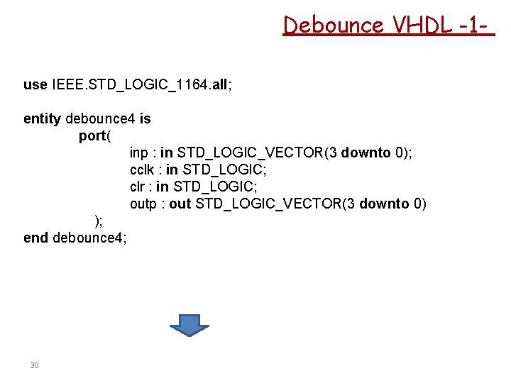
Debounce VHDL -1 use IEEE. STD_LOGIC_1164. all; entity debounce 4 is port( inp : in STD_LOGIC_VECTOR(3 downto 0); cclk : in STD_LOGIC; clr : in STD_LOGIC; outp : out STD_LOGIC_VECTOR(3 downto 0) ); end debounce 4; 30

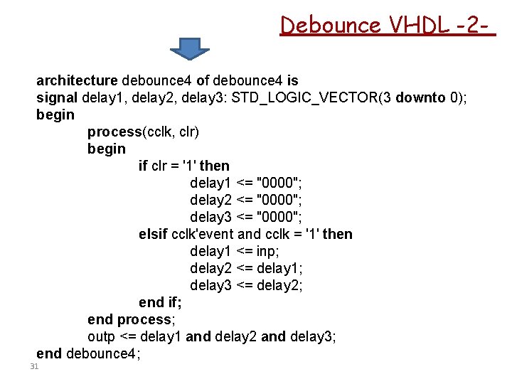
Debounce VHDL -2 architecture debounce 4 of debounce 4 is signal delay 1, delay 2, delay 3: STD_LOGIC_VECTOR(3 downto 0); begin process(cclk, clr) begin if clr = '1' then delay 1 <= "0000"; delay 2 <= "0000"; delay 3 <= "0000"; elsif cclk'event and cclk = '1' then delay 1 <= inp; delay 2 <= delay 1; delay 3 <= delay 2; end if; end process; outp <= delay 1 and delay 2 and delay 3; end debounce 4; 31

Simulation of VHDL program Bouncing Clean signal It is important to use a low frequency for cclk to make sure all debounces are eliminated. 32

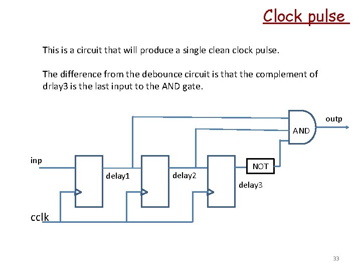
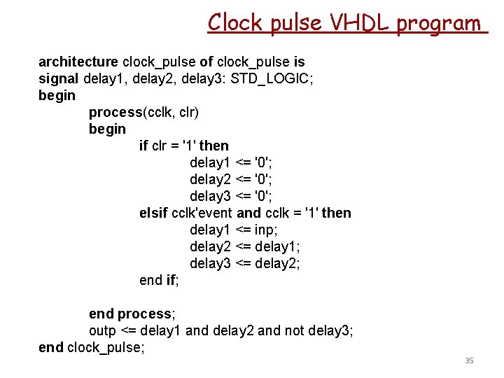
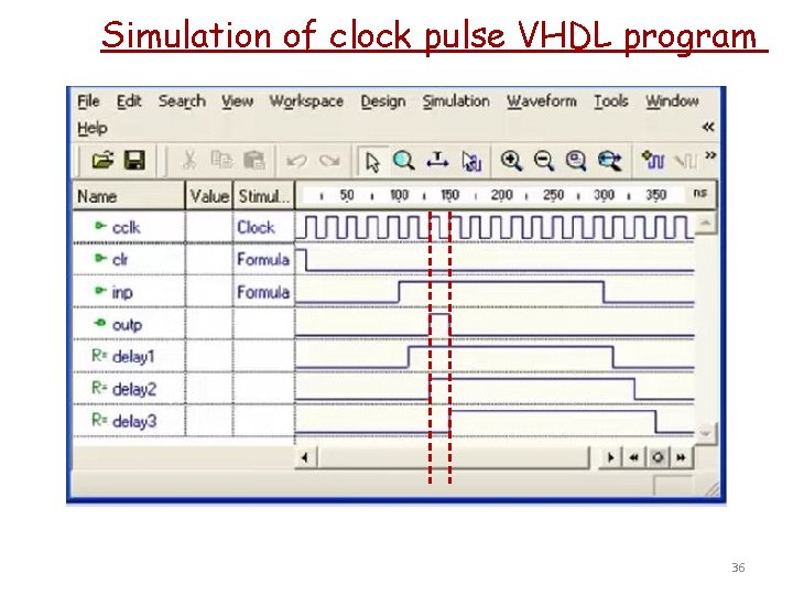
Clock pulse This is a circuit that will produce a single clean clock pulse. The difference from the debounce circuit is that the complement of drlay 3 is the last input to the AND gate. outp AND inp delay 1 delay 2 NOT delay 3 cclk 33

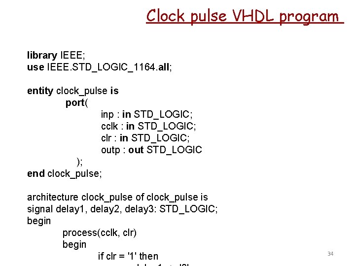
Clock pulse VHDL program library IEEE; use IEEE. STD_LOGIC_1164. all; entity clock_pulse is port( inp : in STD_LOGIC; cclk : in STD_LOGIC; clr : in STD_LOGIC; outp : out STD_LOGIC ); end clock_pulse; architecture clock_pulse of clock_pulse is signal delay 1, delay 2, delay 3: STD_LOGIC; begin process(cclk, clr) begin if clr = '1' then 34

Clock pulse VHDL program architecture clock_pulse of clock_pulse is signal delay 1, delay 2, delay 3: STD_LOGIC; begin process(cclk, clr) begin if clr = '1' then delay 1 <= '0'; delay 2 <= '0'; delay 3 <= '0'; elsif cclk'event and cclk = '1' then delay 1 <= inp; delay 2 <= delay 1; delay 3 <= delay 2; end if; end process; outp <= delay 1 and delay 2 and not delay 3; end clock_pulse; 35

Simulation of clock pulse VHDL program 36

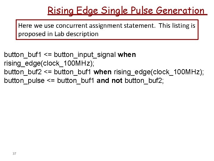
Rising Edge Single Pulse Generation Here we use concurrent assignment statement. This listing is proposed in Lab description button_buf 1 <= button_input_signal when rising_edge(clock_100 MHz); button_buf 2 <= button_buf 1 when rising_edge(clock_100 MHz); button_pulse <= button_buf 1 and not button_buf 2; 37