A DISRUPTOR TO THE SEMICONDUCTOR INDUSTRY THE MONOLITHIC


")


 is already exhibiting diminishing returns Ø The road")


3 D Technology” Business Wire December")


 is better than 2 D ICs")

")
 The Technology Behind SOI Hydrogen Oxide p- Si Top layer Bottom")


 dummy gates, replace with")


 without Heating the Bottom Layers")


 Network (“PDN”) also for heat removal")
 Hai Wei,")
")
 Network Provide effective Heat Removal Path")
- Slides: 57
A DISRUPTOR TO THE SEMICONDUCTOR INDUSTRY THE MONOLITHIC 3 D-IC Monolith. IC 3 D Inc. Patents Pending 1
Agenda: Ø The Semiconductor future is exciting Ø But we are reaching an inflection point Ø Monolithic 3 D IC – the emerging path for the next generation technology driver Ø The challenge and solution for the fabrication of monolithic 3 D IC
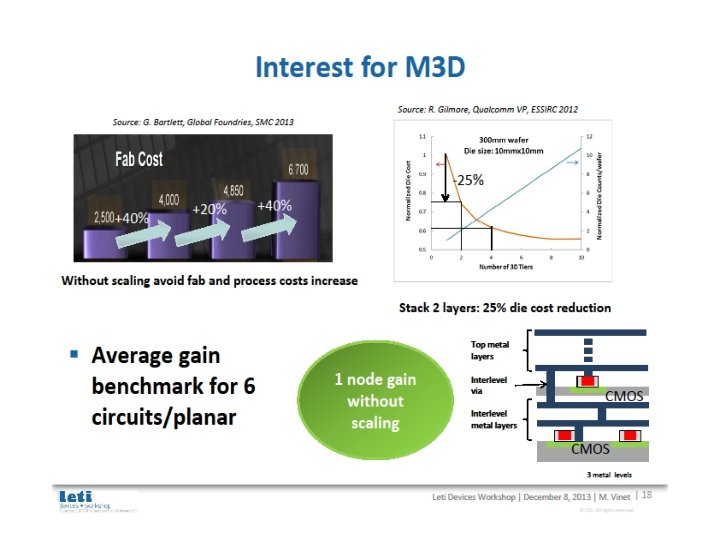
$15 -34 trillion, annual =>~$5 T Semi /year Source: Mc. Kinsey Global Institute Analysis 2013
Cisco sees $19 Trillion opportunity in Io. T “CES LIVE: Cisco's Chambers Says Internet of Everything, $19 Trillion Opportunity, Is Next Big Thing” 1/7/14 <ttp: //www. forbes. com/sites/connieguglielmo/2014/01/07/ces-live-cisco-ceo-chambers-to-deliver-keynote/> $19 trillion: that’s the opportunity he says for the Internet of Everything in the private and public sector combined. Breakout is $14. 4 trillion in private sector and $4. 6 trillion in public sector of new revenue generation or new savings. That’s a conservative number he says for public sector. “This will be bigger than anything done in high tech in a decade. ” “As many as 50 billion devices will be connected to the Internet by 2020, creating a $14. 4 trillion business opportunity” said Rob Lloyd, president of sales and development at Cisco, <http: //www. eetimes. com/electronics-news/4409928/Cisco-sees--14 -trillionopportunity-in-Internet-of-Things>
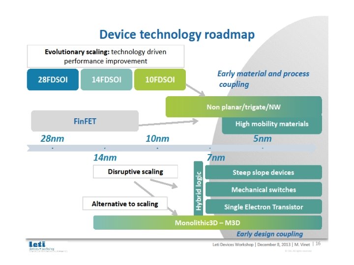
Semiconductor Industry is Facing an Inflection Point Dimensional Scaling has reached Diminishing Returns
The Current 2 D-IC is Facing Escalating Challenges - I Ø On-chip interconnect is Ø Dominating device power consumption Ø Dominating device performance Ø Penalizing device size and cost
Interconnect Delay A Big Issue with Scaling Source: ITRS Ø Transistors improve with scaling, interconnects do not Ø Even with repeaters, 1 mm wire delay ~50 x gate delay at 22 nm node Monolith. IC 3 D Inc. Patents Pending 7
Connectivity Consumes 70 -80% of Total Power @ 22 nm Repeaters Consume Exponentially More Power and Area Ø At 22 nm, on-chip connectivity consumes 70 -80% of total power Ø Repeater count increases exponentially Ø At 45 nm, repeaters are > 50% of total leakage Monolith. IC 3 D Inc. Patents Pending Source: IBM POWER processors R. Puri, et al. , SRC Interconnect Forum, 2006
The Current 2 D-IC is Facing Escalating Challenges - II Ø Lithography is Ø Ø Dominating Fab cost Dominating device cost and diminishing scaling’s benefits Dominating device yield Dominating IC development costs
A Challenge: Lithography Quad-patterning next year costly. EUV delayed, costly. Can we get benefits of scaling without relying on lithography? Monolith. IC 3 D Inc. Patents Pending 10
Martin van den Brink -EVP & CTO, ASML ISSCC 2013 & Semicon. West 2013
Embedded SRAM isn’t Scaling Beyond 28 nm (1. 1 x instead off 4 x) e. SRAM > 60% of Die Area => End of Dimension Scaling ! Dinesh Maheshwari, CTO, Memory Products Division at Cypress Semiconductors, ISSCC 2014
Embedded SRAM isn’t Scaling Beyond 28 nm e. SRAM > 60% of Die Area => End of Dimensional Scaling ! * *imec’s 2013 International Technology Forum,
Moore's Law Dead by 2022* Bob Colwell, Director MTO, DARPA *http: //www. eetimes. com/document. asp? doc_id=1319330 *CRA/CCC & ACM SIGDA, Pittsburgh, March 2013
Conclusions: Ø Dimensional Scaling (“Moore’s Law”) is already exhibiting diminishing returns Ø The road map beyond 2017 (7 nm) is unclear Ø While the research community is working on many interesting new technologies (see below), none of them seem mature enough to replace silicon for 2019 - Carbon nanotube - Graphene - Nanowire - Photonics - Indium gallium arsenide - Spintronics - Molecular computing - Quantum computing -’ 2 D’ devices: Mo. S 2, etc Ø 3 D IC is considered, by all, as the near term solution, and Monolithic 3 D IC is well positioned to be so, as it uses the existing infrastructure Ø It is safe to state that Monolithic 3 D is the only alternative that could be ready for high volume in 2019
CMOS is the Best Device Option
3 D and EDA need to make up for Moore’s Law, says Qualcomm* Ø “Qualcomm is looking to monolithic 3 D and smart circuit architectures to make up for the loss of traditional 2 D process scaling as wafer costs for advanced nodes continue to increase. . . Now, although we are still scaling down it’s not cost-economic anymore” Ø “Interconnect RC is inching up as we go to deeper technology. That is a major problem because designs are becoming interconnect-dominated. Something has to be done about interconnect. What needs to be done is monolithic three-dimensional ICs. ” Ø “TSV. . . are not really solving the interconnect issue I’m talking about. So we are looking at true monolithic 3 D. You have normal vias between different stacks. ” * Karim Arabi Qualcomm VP of engineering Key Note DAC 2014 <http: //www. techdesignforums. com/blog/2014/06/05/karim-arabi-monolithic-3 dic-dac-2014/>
“CEA-Leti Signs Agreement with Qualcomm to Assess Sequential (monolithic)3 D Technology” Business Wire December 08, 2013 “Monolithic 3 D (M 3 D) is an emerging integration technology poised to reduce the gap significantly between transistors and interconnect delays to extend the semiconductor roadmap way beyond the 2 D scaling trajectory predicted by Moore’s Law. ” Geoffrey Yeap, VP of Technology at Qualcomm, Invited paper, IEDM 2013
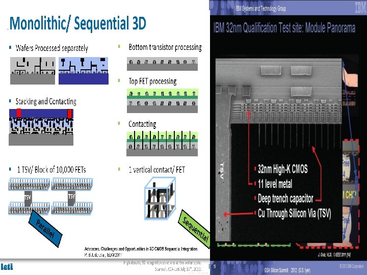
Two Types of 3 D Technology 3 D-TSV Monolithic 3 D Transistors made on separate wafer @ high temperature, then thin + align + bond Transistors made monolithically atop wiring (@ sub-400 o. C for logic) 10 um 50 um 100 nm TSV pitch > 1 um* TSV pitch ~ 50100 nm * [Reference: P. Franzon: Tutorial at IEEE 3 D-IC Conference 2011] 21
MONOLITHIC 10, 000 x 10, 000 the Vertical Connectivity of TSV Enables: TSV Monolithic Layer Thickness ~50 m ~50 nm Via Diameter ~5 m ~50 nm Via Pitch ~10 m ~100 nm Wafer (Die) to Wafer Alignment ~1 m ~1 nm Overall Scale micro ns nanometers Monolith. IC 3 D Inc. Patents Pending 22
3 D ICs in older process (65 nm) is better than 2 D ICs built with a newer process (32 nm) *IEEE IITC 11 Kim
The Monolithic 3 D Challenge Why is it not already in wide use? Ø Processing on top of copper interconnects should not make the copper interconnect exceed 400 o. C Ø How to bring mono-crystallized silicon on top at less than 400 o. C Ø How to fabricate state-of-the-art transistors on top of copper interconnect and keep the interconnect below at less than 400 o. C Ø Misalignment of pre-processed wafer to wafer bonding step is ~1 um Ø How to achieve 100 nm or better connection pitch Ø How to fabricate thin enough layer for inter-layer vias of ~50 nm Monolith. IC 3 D Inc. Patents Pending 26
Monolith. IC 3 D – Breakthrough 3 Classes of Solutions (3 Generations of Innovation) Ø RCAT (2009) – Process the high temperature on generic structures prior to ‘smart-cut’, and finish with cold processes – Etch & Depositions Ø Gate Replacement (2010) (=Gate Last, HKMG) - Process the high temperature on repeating structures prior to ‘smartcut’, and finish with ‘gate replacement’, cold processes – Etch & Depositions Ø Laser Annealing (2012) – Use short laser pulse to locally heat and anneal the top layer while protecting the interconnection layers below from the top heat
Layer Transfer (“Ion-Cut”/“Smart-Cut”) The Technology Behind SOI Hydrogen Oxide p- Si Top layer Bottom layer anneal or sideways bond to bottom of top layer p- Si Oxide Flip top layer and implant Oxide Cleave using 400 o. C mechanical force. layer H p. Si Oxide CMP. H Similar process (bulk-to-bulk) used for manufacturing all SOI wafers today p- Si Oxide
Monolith. IC 3 D - 3 Classes of Solutions Ø RCAT – Process the high temperature on generic structure prior to ‘smart-cut’, and finish with cold processes – Etch & Depositions Ø Gate Replacement (=Gate Last, HKMG) - Process the high temperature on repeating structure prior to ‘smart-cut’, and finish with ‘gate replacement’, cold processes – Etch & Depositions Ø Laser Annealing – Use short laser pulse to locally heat and anneal the top layer while protecting the interconnection layers below from the top heat
Step 1. 1 Donor Layer Processing Step 1 - Implant and activate unpatterned N+ and P- layer regions in standard donor wafer at high temp. (~900 o. C) before layer transfer. Oxidize (or CVD oxide) top surface. PN+ P- Si. O 2 Oxide layer (~100 nm) for oxide -to-oxide bonding with device wafer. Step 2 - Implant H+ to form cleave plane for the ion cut PN+ P- Monolith. IC 3 D Inc. Patents Pending H+ Implant Cleave Line in N+ or below 30
Step 3 - Bond and Cleave: Flip Donor Wafer and Bond to Processed Device Wafer Cleave along H+ implant line using 400 o. C anneal or sideways mechanical force. Si. O 2 with bond. CMP. Polish layers on base and donor wafers (alignment not an issue with blanket wafers) - Silicon N+ <200 n m) P- Processed Base IC Monolith. IC 3 D Inc. Patents Pending 31
Step 4 - Etch and Form Isolation and RCAT Gate • Litho patterning with features aligned to bottom layer • Etch shallow trench isolation (STI) and gate structures Gate • Deposit Si. O 2 in STI Oxide • Grow gate with ALD, etc. at low temp (<350º C oxide or high-K metal gate) Ox Advantage: PThinned donor wafer is transparent to litho, enabling direct alignment to device wafer alignment marks: no indirect alignment. (common +N for TSV 3 DIC) Monolith. IC 3 D Inc. Patents Pending Isolatio n Gate Ox Processed Base IC 32
Step 5 – Etch Contacts/Vias to Contact the RCAT Ø Complete transistors, interconnect wires on ‘donor’ wafer layers Ø Etch and fill connecting contacts and vias from top layer aligned to bottom layer +N P- Processed. Base Processed ICIC Monolith. IC 3 D Inc. Patents Pending 33
Monolith. IC 3 D - 3 Classes of Solutions Ø RCAT – Process the high temperature on generic structure prior to ‘smart-cut’, and finish with cold processes – Etch & Depositions Ø Gate Replacement (=Gate Last, HKMG) - Process the high temperature on repeating structure prior to ‘smart-cut’, and finish with ‘gate replacement’, cold processes – Etch & Depositions Ø Laser Annealing – Use short laser pulse to locally heat and anneal the top layer while protecting the interconnection layers below from the top heat
A Gate-Last Process for Cleave and Layer Transfer NMO S Donor wafer Device wafer PMO S Poly Oxide ØFully constructed transistors attached to each other; no blanket films Ø proprietary methods align top layer atop bottom layer Monolith. IC 3 D Inc. Patents Pending 35
A Gate-Last Process for Cleave and Layer Transfer Step 4. Step 3. 3 Ø Bond to temporary carrier wafer (adhesive or oxideto-oxide) Ø Cleave along cut line Ø CMP to STI Implant H for cleaving NMO S PMO S Carrie r STI H+ Implant Cleave Line CMP to STI Monolith. IC 3 D Inc. Patents Pending 36
A Gate-Last Process for Cleave and Layer Transfer Carri er Oxideoxide bond NMO S PMO S Foundatio n Monolith. IC 3 D Inc. Patents Pending Step 5. Ø Low-temp oxide deposition Ø Bond to bottom layer Ø Remove carrier 37
A Gate-Last Process for Cleave and Layer Transfer Remove (etch) dummy gates, replace with HKMG Step 6. On transferred layer: Ø Etch dummy gates Ø Deposit gate dielectric and electrode Ø CMP Ø Etch tier-to-tier vias thru STI Ø Fabricate BEOL interconnect NMO S PMO S Monolith. IC 3 D Inc. Patents Pending 38
Path 2 – Leveraging Gate Last + Innovative Alignment Ø Misalignment of preprocessed wafer to wafer bonding step is ~1 um ØHow to achieve 100 nm or better connection pitch ØHow to fabricate thin enough layer for inter 1 m Misalignment layer vias of ~50 nm Monolith. IC 3 D Inc. Patents Pending 39
Novel Alignment Scheme using Repeating Layouts Oxide Landing pad Bottom layer layout Top layer layout Throughlayer connectio n Ø Even if misalignment occurs during bonding repeating layouts allow correct connections Ø Above representation simplistic (high area penalty) Monolith. IC 3 D Inc. Patents Pending 40
A More Sophisticated Alignment Scheme Oxide Landing pad Bottom layer layout Top layer layout Monolith. IC 3 D Inc. Patents Pending Through -layer connecti on 41
Monolith. IC 3 D - 3 Classes of Solutions Ø RCAT – Process the high temperature on generic structures prior to ‘smart-cut’, and finish with cold processes – Etch & Depositions Ø Gate Replacement (=Gate Last, HKMG) - Process the high temperature on repeating structures prior to ‘smart-cut’, and finish with ‘gate replacement’, cold processes – Etch & Depositions Ø Laser Annealing – Use short laser pulse to locally heat and anneal the top layer while protecting the interconnection layers below from the top heat
Annealing Trend with Scaling
LSA 100 A – Short Pulse, Small Spot Dwell time ~ 275µs
Two Major Semiconductor Trends help make Monolithic 3 D Practical NOW Ø As we have pushed dimensional scaling: Ø The volume of the transistor has scaled Ø Bulk um-sized transistors FDSOI & Fin. Fet nm Ø Processing times have trended lower Ø Shallower & sharper junctions, tighter pitches, etc. => Much less to heat and for much shorter time
The Top Layer has a High Temperature >1000 C) without Heating the Bottom Layers (<400°C) !!! } >1000°C } <400°C
Process Window Set to Avoid Damage Temperature variation at the 20 nm thick Si source/drain region in the upper active layer during laser annealing. Note that the shield layers are very effective in preventing any large thermal excursions in the lower layers
The Monolithic 3 D Advantage II. Reduction die size and power – doubling transistor count - Extending Moore’s law Monolithic 3 D is far more than just an alternative to 0. 7 x scaling !!! III. Significant advantages from using the same fab, design tools IV. Heterogeneous Integration V. Multiple layers Processed Simultaneously - Huge cost reduction (Nx) VI. Logic redundancy => 100 x integration made possible VII. Enables Modular Design VIII. Naturally upper layers are SOI IX. Local Interconnect above and below transistor layer X. Re-Buffering global interconnect by upper strata XI. Others A. Image sensor with pixel electronics B. Micro-display
Monolithic 3 D Provides an Attractive Path to… Monolithic 3 D Integration with Ion-Cut Technology 3 D-CMOS: Monolithic 3 D Logic Technolog LOGIC 3 D-FPGA: Monolithic 3 D Programmable L 3 D-Gate. Array: Monolithic 3 D Gate Array 3 D-Repair: Yield recovery for high-density Can be applied to many market segments MEMOR Y 3 D-DRAM: Monolithic 3 D DRAM 3 D-RRAM: Monolithic 3 D RRAM 3 D-Flash: Monolithic 3 D Flash Memory OPTOELECTRONI CS 3 D-Imagers: Monolithic 3 D Image Sensor 3 D-Micro. Display: Monolithic 3 D Display 3 D-LED: Monolithic 3 D LED Monolith. IC 3 D Inc. Patents Pending 50
Summary Ø Monolithic 3 D is now practical and well positioned to keep Moore’s Law alive for many years Ø Multiple paths to process mono-crystal transistors over copper interconnect Ø Monolithic 3 D IC provides many opportunities for existing products and for new products & architectures
Back Ups
The Operational Thermal Challenge Ø Upper tier transistors are fully surrounded by oxide and have no thermal path to remove operational heat away Poor Heat Conduction ~1 W/m. K Good Heat Conduction ~100 W/m. K
The Solution Ø Use Power Delivery (Vdd, Vss) Network (“PDN”) also for heat removal Ø Add heat spreader to smooth out hot spots Ø Add thermally conducting yet electrically nonconducting contacts to problem areas such as transmission gates
IEDM 2012 Paper Cooling Three-Dimensional Integrated Circuits using Power Delivery Networks (PDNs) Hai Wei, Tony Wu, Deepak Sekar+, Brian Cronquist*, Roger Fabian Pease, Subhasish Mitra Stanford University, Rambus+, Monolithic 3 D Inc. * 5
Monolithic 3 D Heat Removal Architecture (Achievable with Monolithic 3 D vertical interconnect density) px Signal wire py Heat sink Ø Global power grid shared among multiple device layers, local power grid for each device layer Ø Local VDD grid architecture shown above Ø Optimize all cells in library to have low thermal resistance to VDD/VSS lines (local heat sink) Patented and Patent Pending Technology Without Power Grid With Power Grid
Power Delivery (Vdd, Vss) Network Provide effective Heat Removal Path