EMT 272 Semiconductor Fundamentals SEMICONDUCTOR PHYSICS Carrier Transport


 DRIFT The movement of carrier due to electric field, E")


 applied to an")


 At thermal equilibrium b) Under bias condition")

, length (L), carrier concentration of")


![Carrier Diffusion EINSTEIN RELATION Ø Equation of [4] can be written using theorem of](https://slidetodoc.com/presentation_image_h/c118b4dee0b64e5aa07a58c261ff3137/image-37.jpg "Carrier Diffusion EINSTEIN RELATION Ø Equation of [4] can be written using theorem of")
 are injected into homogeneous n-type semiconductor sample. An electric")


")
- Slides: 53
EMT 272 Semiconductor Fundamentals SEMICONDUCTOR PHYSICS Carrier Transport Phenomena
Outlines: Carrier Drift Carrier Diffusion Generation & Recombination Process Continuity Equation Thermionic Emission Process Tunneling Process High-Field Effect
Part 1: Carrier Drift Carrier Diffusion Generation & Recombination Process
• The net flow of electrons and holes in s/cond will generate current. • The process by these charged particles (electrons/holes) move is called transport • Carrier transport determine the current-voltage characteristics of s/cond devices • Electrical properties (IV characteristics)
CARRIER TRANSPORT (PART 1) DRIFT The movement of carrier due to electric field, E DIFFUSION The flow of carrier due to density gradients (dn/dx)
GENERATION & RECOMBINATION The process by which mobile charged carriers are created and eliminated
Carrier Drift
Carrier Drift MOBILITY • • Measure of how quickly an electron can move through a metal or semiconductor in presence of electrical field. Semiconductor mobility depends on the impurity concentrations (including donor and acceptor concentrations), defect concentration, temperature, and electron and hole concentrations Consider an n-type semiconductor sample with uniform donor concentration in thermal equilibrium. -As discussed in earlier chapter, conduction electrons in the CB are free particles, since they are not associated with any lattice or donor site. -Influence of crystal lattices is incorporated in the effective mass of conduction electrons, which differs somewhat from the mass of free electron.
Ø Under thermal equilibrium / No applied electric filed § Electrons in semiconductor are moving rapidly in all direction, where thermal motion of an individual electron may be visualized as a succession of random scattering from collisions with lattice atoms, impurity atoms, and other scattering centers (Figure a) Ø Random motion of electrons lead to zero net displacement. Ø The average distance between collisions : MEAN FREE PATH Ø The average time between collisions: MEAN FREE TIME, C Schematic path of random thermal motion of electron in semiconductor.
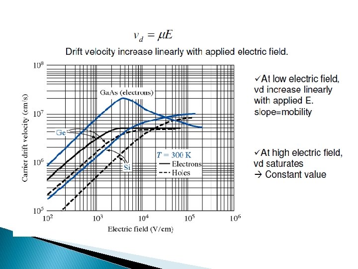
When small electric field, ɛ, is applied to semiconductor sample, each electron will experience a force (–q. E) from the field and will be accelerated along the field (in opposite direction to the field) during the time between collisions. Therefore, an additional thermal velocity component will be superimposed upon thermal motion of electron. This additional component called DRIFT VELOCITY Net displacement of the electron is in the opposite direction of applied field. Combined motion due to random thermal motion and an applied electric field
Thermal equilibrium Ø Random motion of carrier without applied field. Ø No net carrier displacement Ø Random thermal velocity, Vth Applied electric filed Ø Random motion as well as a net movement along the of field (in the opposite direction of filed). Ø Net carrier displacement and thus a net velocity along the field. Ø This velocity is called a DRIFT VELOCITY, which gives drift current.
Ø Drift Velocity, vn by equating the momentum (force x time) applied to an electron during the free flight between collisions to the momentum gained by the electron in the same period. Ø The equality is valid because in the steady state all momentum gained between collision is lost to the lattice in the collision. Ø Therefore, the momentum applied to an electron, -q. E C is equal to the Momentum gained by an electron: mnvn. Where Electron drift velocity Hole drift velocity
Mobility is related directly to mean free time between collisions determined by the various scattering mechanism. Two MOST important mechanisms: lattice scattering and impurity scattering. LATTICE SCATTERING results from thermal vibrations of the lattice atoms at any temperature above absolute temperature, T>0 K. Since lattice vibration increase with increase of temperature, lattice scattering becomes dominant at high temp. Hence, mobility decreases with increasing temp. theoretically mobility due to lattice scattering L decrease in proportion to T-3/2 • • IMPURITY SCATTERING • • • results when charge carrier travels past an ionized doping impurity (donor or acceptor). Depends on Coulomb force interaction. Probability of impurity scattering depends on total concentration of ionization impurities (sum of +ve and –ve charge ions). It becomes less significant at higher temperatures. At higher temperature, the carrier move faster; they remain near the impurity atom for a shorter time and are therefore less effectively scattered
The probability of a collision taking place in unit time, 1/ C, is the sum of the probabilities of collision due to the various scattering mechanism: or L – lattice scattering mobility I – impurity scattering mobility
Light doped Temperature dependence of mobility Electron mobility in silicon vs temperature for various donor concentration Heavy doped For lightly doping (i. e. 1014 cm-3) – lattice scattering dominates and mobility decreases as the temperature increases. For heavily doping (i. e. 1019 cm-3) impurity scattering is most pronounced at low temperature. Mobility increases as temperature increases. For a given temperature, mobility decreases with increasing impurity concentration (due to enhanced impurity scattering).
Doping dependence of mobility in Si and Ga. As ¡ Mobility reaches a maximum value at low impurity concentrations corresponds to the lattice scattering limitation. ¡ Both electron & hole mobility decrease with increasing impurity concentration. ¡ Mobility of electrons is greater than holes due to the smaller effective mass of electrons.
EXAMPLE 1: Calculate the mean free time and mean free path of an electron having mobility 1000 cm 2/V-s at 300 K. Given mn = 0. 26 m 0, m 0 = 0. 91 x 10 -30 kg, q = 1. 6 x 10 -19 C, vth = 107 cm/s SOLUTION: Mean free time, using this equation: C = 1. 48 x 10 -13 s = 0. 148 ps Mean free path, l = vth x C l = 14. 8 nm
Carrier Drift CONDUCTIVITY AND RESISTIVITY Ø Consider conduction in homogeneous semiconductor material. Ø Assume that contacts (Figures (b) at next slides) are ohmic, thus there is negligible voltage drop at each of the contacts. Will discussed ohmic contact in other chapter. Ø When electric field E is applied to a semiconductor , electron will experience a force –q. E. Ø The force is equal to the negative gradient of potential energy.
a) At thermal equilibrium b) Under bias condition
Homogeneous semiconductor Ø Under bias condition, electrons move to the right side. Kinetic energy corresponds to the distance from the band edge. Ø When an electron undergoes a collisions, it loses some or all of its kinetic energy to the lattice and drops toward its thermal equilibrium position. Ø After the electron lost some or all of kinetic energy, it will begin to move toward the right and the same process repeated many times. Ø Conduction hole is in similar manner but opposite direction. Ø Transport of carrier under the influence of electric field produces a current called the DRIFT CURRENT
Ø Consider a semiconductor sample with cross section (A), length (L), carrier concentration of n electrons/cm 3. Suppose an electric field, ɛ is applied to the sample. Ø CURRENT DENSITY for electron - Summing the product of charge (q) on each electron times the electron’s velocity over all electrons per unit volume n. Current conduction is a uniformly doped semiconductor bar with length L and cross section A
• Similar argument applied to holes. • TOTAL CURRENT flowing in the semiconductor • CONDUCTIVITY • RESISTIVITY • EXTRINSIC RESISTIVITY For n-type semiconductor ( n>>p) For p-type semiconductor ( p>>n)
At room temperature and low impurity concentration, the carrier concentration = impurity concentration
EXAMPLE 2: b, µp = 505, n = p = ni = 9. 65 109 at T=300 K SOLUTION:
Carrier Drift HALL EFFECT Ø The Hall effect is the production of a voltage difference (the Hall voltage) across an electrical conductor, transverse to an electric current in the conductor and a magnetic field perpendicular to the current. Ø Is used to measure carrier concentration. Ø The most convincing method to show the existence of holes as charge carriers, because the measurement give directly the carrier type.
Ø For p-type semiconductor shown in Figure below. Ø Lorentz force F = qv x B due to the magnetic field will exert an average upward force on the holes flowing in the x –direction. Ø The upward directed current causes an accumulation of holes at the top of the sample that rise to a downward electric field, Ey. Ø No net current flow along the y-direction in the steady state, electric field along y-axis balance the Lorentz force. Ø Therefore, or (Hall field) Ø The establishment of the electric field is known as Hall effect Ø Terminal voltage, VH = ɛy. W (Hall Voltage)
Ø From the hole drift velocity equation, and Ø Therefore, HALL FIELD, • where RH (HALL COEFFICIENT) : Ø Similar result can be obtained for an n-type semiconductor, Ø Measurement of Hall voltage for a known current and magnetic field:
EXAMPLE 3: A sample of Si is doped with 1016 phosphorus atoms/cm 3. Find the Hall voltage in a sample with W = 500 µm, A = 2. 5 x 10 -3 cm 2, I = 1 m. A and Bz = 10 -4 Wb/cm 2. SOLUTION: The Hall Coefficient, RH = -1/qn = -625 cm 3/C. The Hall Voltage, VH = ɛy. W = (RH x (I/A) x Bz)W = -1. 25 m. V
Carrier Diffusion
Carrier Diffusion DIFFUSION PROCESS Ø If there is a spatial variation of carrier concentration in the semiconductor material, the carriers tend to move from a region of high concentration to a region of low concentration. This current component is called DIFFUSION CURRENT.
Ø Ø Ø When semiconductor is at uniform temperature, average thermal energy of electrons does not vary with x, only density n (x) varies. Consider electrons cross the plane at x =0 per unit time per unit area. Because of finite temperature, electrons have random thermal motion with thermal velocity, vth and mean free path, l (l = vth C ) Electrons at x =-l (on the left side), have equal chances to move left/right In a mean free time, C , one half will move across the plane x =0. Therefore, average rate of electron flow per unit area F 1 of electron crossing plane x = 0 from the left is: [1]
Ø The average rate of electron flow per unit area F 2 of electrons at x=l crossing plane (from the right) [2] Ø The net rate of carrier flow Ø Due to approximation the densities at x = ± l by the first two terms of Taylor series expansion, [3] Ø Where Dn = Vthl is call diffusion coefficient / diffusivity
Ø Each electron carriers a charge -q, therefore the carrier flow gives rise to a current is: [4]
EXAMPLE 4: Assume that n type s/cond at T=300 K, the electron concentration varies linearly 1 x 10¹⁸ to 7 x 1017 cm-3 over a distance of 0. 1 cm. Calculate the diffusion current density if the electron diffusion coefficient is Dn = 22. 5 cm 2/s SOLUTION: The diffusion current density = 10. 8 A/cm 2
Carrier Diffusion EINSTEIN RELATION Ø Equation of [4] can be written using theorem of equipartition of energy for this 1 D case. [6] Ø as we know: Ø Einstein relation can be written as Ø or
EXAMPLE 5: Minority carriers (holes) are injected into homogeneous n-type semiconductor sample. An electric field 50 V/cm is applied across the sample, and the field moves these minority carriers a distance 1 cm in 100 um. Find the drift velocity and the diffusivity of the minority carriers. SOLUTION: drift velocity, vp =1 cm/ (100 x 10 -6 s) = 10 4 cm/s Mobility, µp = vp/ɛ = (10 4 cm/s) / (50 V/cm) = 200 cm 2/V-s Diffusivity, Dp = (k. T/q) µp = 0. 0259 x 200 = 5. 18 cm 2/s
Carrier Diffusion CURRENT DENSITY EQUATIONS Ø When an electric field is present in addition to a concentration gradient, both drift current and diffusion current will flow. Ø The total current density at any point is the sum of the drift and diffusion components: Ø current density, Ø similar expression can be obtained for the hole current: the negative is due to diffusion results in a hole current that flows in the negative x-direction. Ø The total conduction current density is
Generation and Recombination
Generation and Recombination DIRECT RECOMBINATION • For direct-bandgap s/cond in thermal equilibrium, the continuous thermal vibration of lattice atoms cause bonds between neighboring atoms to broken. • The thermal energy enables the electron in VB to make transition to the CB, leaving hole in VB. (Bonds broken cause electron-hole pair. ) • CARRIER GENERATION– electron to make upward transition to CB and leaving a hole in VB. It represented by the generation rate Gth (number of electron-hole pair generated • RECOMBINATION – electron makes transition downward from CB. It represented by recombination rate Rth
GENERATION RECOMBINATION At thermal equilibrium, Gth = Rth, so that carrier concentration remain constant and pn = ni 2 is maintained.
• When excess carriers are introduced to direct-bandgap s/cond, high probability that electrons and holes recombine directly. It is because the bottom of CB and top of VB are lined up and no additional momentum is required for transition across the bandgap. • Rate of recombination is proportional to number of electrons available in CB and number of holes available in VB R = βnp • The rate of generation & recombination in n-type is nno & pno – electron and hole densities at equilibrium - proportionality constant
UNDER ILLUMNIATION • When we shine a light, , it produced electron-hole pair at a rate GL, recombination and generation rate. The carrier concentrations are above their equilibrium values. • The rate of generation & recombination • Excess carrier concentration
• The net change of hole concentration • At steady-state, dpn/dt = 0; • At low level injection, pno << nno, the net recombination is p – lifetime of the excess minority carriers. • Net recombination, U: U = (nno + pno + ∆p)∆p It shows that U = excess minority carrier concentration
LIGHT OFF • In steady state, generation rate is given by • In arbitrary time, when the light is turn off, t = 0, the boundary condition • The net rate of change of hole concentration
Generation and Recombination INDIRECT RECOMBINATION • For indirect s/cond, a direct recombination process is unlikely, because the electrons at the bottom of the CB have nonzero momentum with respect to the holes at the top of VB. • Also known as trap-assisted recombination. • A direct transition that conserves both energy and momentum is not possible w/out a simultaneous lattice interaction. • The dominant recombination is INDIRECT TRANSITION via localized energy states in the forbidden energy gap, also known as RECOMBINATION/GENERATION TRAP CENTER.
Indirect generation-recombination process at thermal equilibrium • The charge state of the recombination center must be attractive and efficient. • State close to Ec or Ev is not efficient. • The trap center caused by the presence of foreign atom/structure defect. • Once the trap is filled, can not accept other carrier.
¡ ¡ The recombination rate : Under low-injection condition in a n-type, so nn >> pn , then U can be written as where, vth – thermal velocity, Nt – concentration of the recombination centre, - capture cross section (effectiveness of the centre to capture an electron or hole), and
Generation and Recombination SURFACE RECOMBINATION • Because of abrupt discontinuity of the lattice structure at the surface, a large number of localized energy states or generation-recombination centers maybe introduced at surface region. • The energy states (SURFACE STATES), greatly enhance the recombination rate at surface. • The kinetics of surface recombination are similar in bulk. Total number of carrier recombining at the surface per unit area and unit time: The low-injection surface recombination velocity : where, ps – concentration at surface, Nst – recombination center density per unit area in the surface region.
Schematic diagram of bonds at a clean semiconductor surface. The bonds are anisotropic and differ from those in the bulk.
Generation and Recombination AUGER RECOMBINATION • Occurs by the transfer of the energy and momentum released by the recombination of an electron-hole pair to a third particle that can be either electron/hole. • In figure, the second electron in CB absorbs the energy released by the direct recombination. After the Auger process, the second electron become energetic electron. It loses the energy to the lattice by scattering. • This process is important when the carrier concentration is very high (high doping/high injection level). The rate of this recombination :
NEXT TOPIC: CARRIER CONCENTRATION PHENOMENA (Continuity Equation, Thermionic Emission Process, Tunneling Process, High-Field Effect)