A DISRUPTOR TO THE SEMICONDUCTOR INDUSTRY Precision Bonders

A DISRUPTOR TO THE SEMICONDUCTOR INDUSTRY Precision Bonders - A Game Changer for Monolithic 3 D Zvi Or-Bach, Brian Cronquist, Zeev Wurman, Israel Beinglass, and Albert Henning Monolith. IC 3 D Inc. Paper Monolith. IC 3 D Inc. Patents Pending 11. 3 IEEE S 3 S October 2014 1

Agenda Ø Motivation – The Escalating Challenges of 2 D Scaling Ø Monolithic 3 D as the Solution Ø Emerging Precision Bonders Ø Impact and a Process Flow Ø Advantages of Monolithic 3 DIC 2

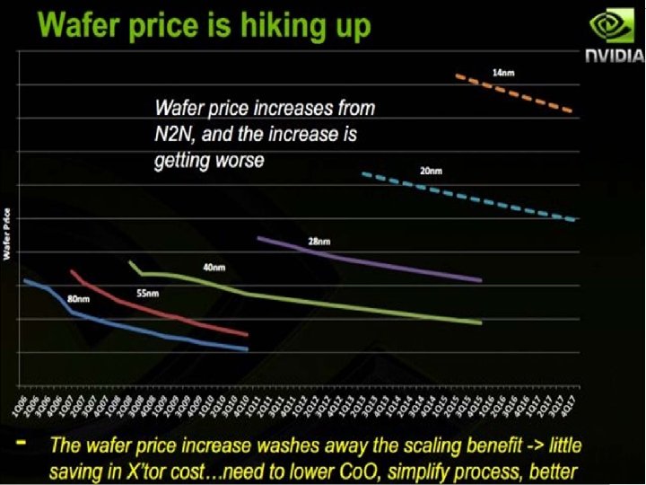

Connectivity Consumes 70 -80% of Total Power @ 22 nm Repeaters Consume Exponentially More Power and Area Ø At 22 nm, on-chip connectivity consumes 70 -80% of total power Ø Repeater count increases exponentially Ø At 45 nm, repeaters are > 50% of total leakage Monolith. IC 3 D Inc. Patents Pending Source: IBM POWER processors R. Puri, et al. , SRC Interconnect Forum, 2006
3 D Technology” Business Wire December")
“CEA-Leti Signs Agreement with Qualcomm to Assess Sequential (monolithic)3 D Technology” Business Wire December 08, 2013 “Monolithic 3 D (M 3 D) is an emerging integration technology poised to reduce the gap significantly between transistors and interconnect delays to extend the semiconductor roadmap way beyond the 2 D scaling trajectory predicted by Moore’s Law. ” Geoffrey Yeap, VP of Technology at Qualcomm, Invited paper, IEDM 2013

MONOLITHIC 10, 000 x 10, 000 the Vertical Connectivity of TSV 8

The Monolithic 3 D Challenge Why is it not already in wide use? Ø Processing on top of copper interconnects should not make the copper interconnect exceed 400 o. C Ø How to bring mono-crystallized silicon on top at less than 400 o. C Ø How to fabricate state-of-the-art transistors on top of copper interconnect and keep the interconnect below at less than 400 o. C Ø Misalignment of pre-processed wafer to wafer bonding step is was ~1µm Ø How to achieve 100 nm or better connection pitch Ø How to fabricate thin enough layer for inter-layer vias of ~50 nm 9
 – Process the high")
Monolith. IC 3 D Precision Bonder Flow Ø RCAT (2009) – Process the high temperature on generic structures prior to ‘smart-cut’, and finish with cold processes – Etch & Depositions Ø Gate Replacement (2010) (=Gate Last, HKMG) - Process the high temperature on repeating structures prior to ‘smartcut’, and finish with ‘gate replacement’, cold processes – Etch & Depositions Ø Laser Annealing (2012) – Use short laser pulse to locally heat and anneal the top layer while protecting the interconnection layers below from the top heat Ø Precise Bonder (2014) – Use precision bonder and prior techniques such as ‘gate replacement’. Offers low cost flow with minimal R&D

Precision Bonder – Breakthrough With Monolth. IC 3 D flow => Easy path to M 3 D Ø Alignment challenge is resolved by the use of Precision Bonder and ‘Smart Alignment’ Ø Achieving 10, 000 x vertical connectivity as the upper strata will be thinner than 100 nm Ø Rich vertical connectivity Ø High performance – low vertical connection RC Ø Low manufacturing costs Ø Utilizing the existing front-end process !!! Patents Pending

Use standard flow to process “Stratum 3” Stratum 3 NMOS Poly Oxide PMOS STI ~700 µm Donor Wafer Patents Pending Silicon 12

Implant H+ 100 nm depth for the ion-cut Ions Implant ~E 17 NMOS PMOS STI ~100 nm H+ ~700µm Donor Wafer Patents Pending Silicon 13

Bond to a carrier-wafer ~700µm Carrier Wafer Oxide to Oxide bond STI H+ ~700µm Donor Wafer Silicon Patents Pending 14
 Donor Wafer off ~700µm Carrier Wafer Transferred ~100 nm")
‘Cut’ (Heating to ~550 ºC) Donor Wafer off ~700µm Carrier Wafer Transferred ~100 nm Layer - Stratum 3 STI Silicon H+ ~700µm Donor Wafer Silicon Patents Pending 15

CMP and repair the transferred layer – high temperature is OK ! STI ~100 nm Silicon Oxide Bond Oxide ’etch stop’ ~700µm Carrier Wafer Patents Pending 16

Use standard flow to process “Stratum 2” Note: High Temperature is OK Stratum 2 ~100 nm Layer High Performance Transistors Oxide Silicon STI Oxide Stratum 3 Bond Oxide ’etch stop’ ~700µm Carrier Wafer Note: A vertical isolation could be formed by reverse bias, deep implant or other methods. Patents Pending 17

Add at least one interconnect layer Stratum 2 Silicon ~100 nm Transferred Layer Stratum 3 Oxide Bond Oxide ’etch stop’ ~700µm Carrier Wafer Patents Pending 18
 Oxide-oxide")
Transfer onto target layer ~700µm Carrier Wafer Transferred Layer (Stratum 2 +Stratum 3) Oxide-oxide bond Base Wafer Patents Pending NMOS Monolith. IC 3 D Inc. Patents Pending PMOS 19
 ~700µm Carrier Wafer Stratum 3 100 nm Stratum 2 Oxide-oxide")
Remove carrier-wafer (grind, etch) ~700µm Carrier Wafer Stratum 3 100 nm Stratum 2 Oxide-oxide bond Base Wafer Patents Pending NMOS Monolith. IC 3 D Inc. Patents Pending PMOS 20
 Stratum 3 Stratum 2 Oxide-oxide bond Base Wafer Patents Pending")
Gate replacements (when applicable) Stratum 3 Stratum 2 Oxide-oxide bond Base Wafer Patents Pending NMOS Monolith. IC 3 D Inc. Patents Pending PMOS 21

Monolithic 3 D using Precise Bonder Ø Utilizes existing transistor process Ø Could help upgrade any fab (leading or trailing) Ø Provides two additional transistor layers Ø Very competitive cost structure Ø Better power, performance, price than a node of scaling at a fraction of the costs !!! Ø Allows functionality that could not be attained by 2 D devices

Connect to “Strata 1” using ‘Smart-Alignment’ Landing pad Bottom layer layout Oxide Top layer layout Through -layer connecti on ‘Smart-Alignment’ Patents Pending 23

Smart Alignment Through Layer Via connected by landing pad of 200 x 200 nm² 200 nm

Smart Alignment

‘Smart-Alignment’ Bottom layer layout Landing pad Vertical connection 1 for 200 nmx 200 nm ‘Smart-Alignment’ Vertical connection 200 nm/metal pitch ~ 20 for 200 nmx 200 nm Ø ~20 X better vertical connectivity Ø Minimum abstraction for routing Patents Pending 26

Sequential vs. Parallel Ø Some people call monolithic 3 D as a ‘sequential process’ in contrast to TSV which is ‘parallel’ Ø Sequential process might over-extend TAT ! Ø By using the Monolith. IC + Fusion Bonder flow, a parallel monolithic flow could be constructed Patents Pending

The Monolithic 3 D Advantage 1. Reduction die size and power – doubling transistor count Extending Moore’s law Monolithic 3 D is far more than just an alternative to 0. 7 x scaling !!! 2. Significant advantages from using the same fab, design tools 3. Heterogeneous Integration 4. Multiple layers Processed Simultaneously - Huge cost reduction (Nx) 5. Logic redundancy => 100 x integration made possible 6. 3 D FPGA prototype, 2 D volume 7. Enables Modular Design 8. Naturally upper layers are SOI 9. Local Interconnect above and below transistor layer 10. Re-Buffering global interconnect by upper strata 11. Others A. Image sensor with pixel electronics B. Micro-display -

Some 3 D Applications Ø Ø Ø Image sensor with pixel electronics 3 D FPGA Ultra Scale integration using M 3 DI Redundancy 1 T SRAM (Zeno) over Logic I/O-SRAM-Logic
 over Fin. FET")
1 T SRAM (Zeno) over Fin. FET

Image Sensor with Pixel Electronics Ø With rich vertical connectivity, every pixel of an image sensor could have its own pixel electronics underneath Patents Pending

The Twin Field-programmable & via-configurable fabric Prototype Phase-3 D Vp HV Programming Transistors Production Phase-2 D Anti-fuses • • • Prototype volumes • Prototype costs Std. logic w/mono-3 D • Patents Pending OTP till design & functions stabilized Specific foundry • • • Production volumes Production costs Standard logic process 1 -Mask customization Backup-foundry capable
 >30 x Area vs. Antifuse/Masked Via SRAM")
FPGA Achilles’ Heel – PIC (Programmable Interconnect) >30 x Area vs. Antifuse/Masked Via SRAM bit SRAM FPGA connectivity elements @ 45 nm Via connectivity element @ 45 nm SRAM bit 4 X 4 X Bidi buffer Via/AF Via. 2 m Area 4 m 2 Ratio to AF 100 Area: 0. 04 m 2 SRAM bit TS buffer 4 X . 2 m Area 2 m 2 Ratio to AF 50 SRAM bit Pass gate 10 X Pitch - 0. 2 m. 2 x. 2= 0. 04 m 2 Area . 5 m 2 Ratio to AF 12 Current FPGAs use primarily pass transistors with a driver. Average area ratio of connectivity element >30

Innovation Enabling ‘Wafer Scale Integration’ – 99. 99% Yield with 3 D Redundancy Gene Amdahl -“Wafer scale integration will only work with 99. 99% yield, which won’t happen for 100 years” (Source: Wikipedia) Ø Swap at logic cone granularity ØServer-Farm in a Box Ø Negligible design and power penalty ØWatson in a Smart Phone Ø Redundant 1 above, no performance penalty Patents Pending Ø…
 –”BICS” Ø Multiple thin")
V. Multiple Layers Processed Simultaneously - Huge Cost Reduction (Nx) –”BICS” Ø Multiple thin layers can be process simultaneously, forming transistors on multiple layers Ø Cost reduction correlates with number of layers being simultaneously processed (2, 4, 8, 16, 32, 64, 128, . . . )

IV. Heterogeneous Integration Ø Logic, Memories, I/O on different strata Ø Optimized process and transistors for the function Ø Optimizes the number of metal layers Ø Optimizes the litho. (spacers, older node) Ø Low power, high speed (sequential, combinatorial) Ø Different crystals – E/O

VII. Enables Modular Design Ø Platform-based design could evolve to: Ø Few layers of generic functions like compute, radios, and one layer of custom design Ø Few layers of logic and memories and one layer of FPGA Ø. . .

Summary Ø We have reached an inflection point Ø Monolithic 3 D IC – The next generation technology driver Ø Breaking News – The barriers are now removed Ø Multiple simple and practical paths to monolithic 3 D exist Ø Monolithic 3 D provides more than just scaling

Backup 39

The Operational Thermal Challenge Ø Upper tier transistors are fully surrounded by oxide and have no thermal path to remove operational heat away Poor Heat Conduction ~1 W/m. K Good Heat Conduction ~100 W/m. K
 Hai Wei,")
IEDM 2012 Paper Cooling Three-Dimensional Integrated Circuits using Power Delivery Networks (PDNs) Hai Wei, Tony Wu, Deepak Sekar+, Brian Cronquist*, Roger Fabian Pease, Subhasish Mitra Stanford University, Rambus+, Monolithic 3 D Inc. * 4
")
Monolithic 3 D Heat Removal Architecture (Achievable with Monolithic 3 D vertical interconnect density) px Signal wire py Heat sink Ø Global power grid shared among multiple device layers, local power grid for each device layer Ø Local VDD grid architecture shown above Ø Optimize all cells in library to have low thermal resistance to VDD/VSS lines (local heat sink) Patents Pending Without Power Grid With Power Grid
- Slides: 43