Present and Future Prospects of Semiconductor Industry In
- Slides: 60

Present and Future Prospects of Semiconductor Industry In Malaysia By Ramzan Mat Ayub Timbalan Dekan, Unit R&D, Uni. MAP Azlan Zakaria Head of MEMS and CMOS Group Mimos Berhad School of Microelectronic Engineering

Presentation Outline q The Evolution of Semiconductor Technology q Industry Structure q Technology Challenges & Trends q Semiconductor Industry in Malaysia School of Microelectronic Engineering

The Evolution of Semiconductor Technology School of Microelectronic Engineering

What is Semiconductor Technology? q The technology to produce IC microchips q IC chips are the backbone of the computer industry and have spurred related technologies such as software and internet q Every product of the information age is an offspring of IC technology q IC chips increasingly control functions in cars, TVs, VCRs, cameras, mobile phones, toys, etc. School of Microelectronic Engineering

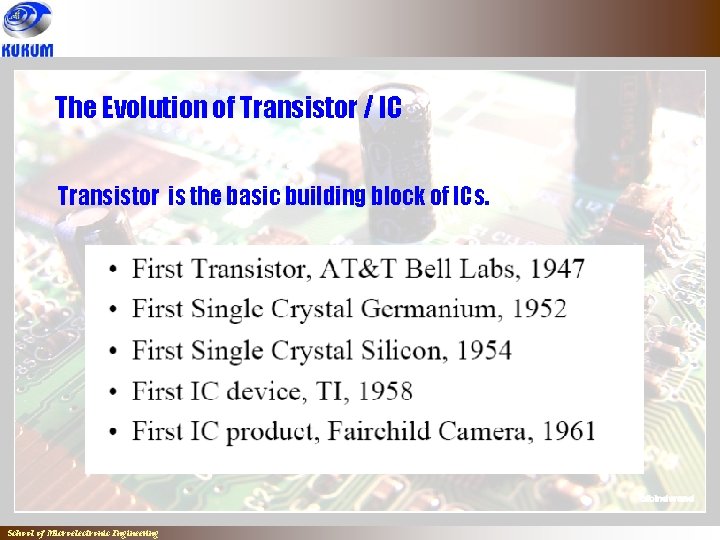
The Evolution of Transistor / IC Transistor is the basic building block of ICs. School of Microelectronic Engineering

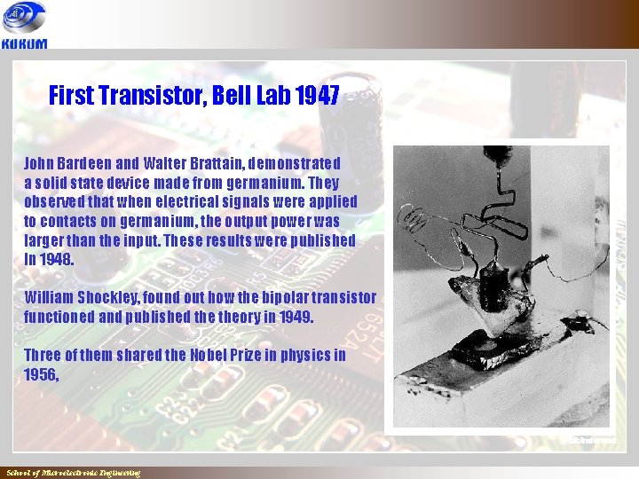
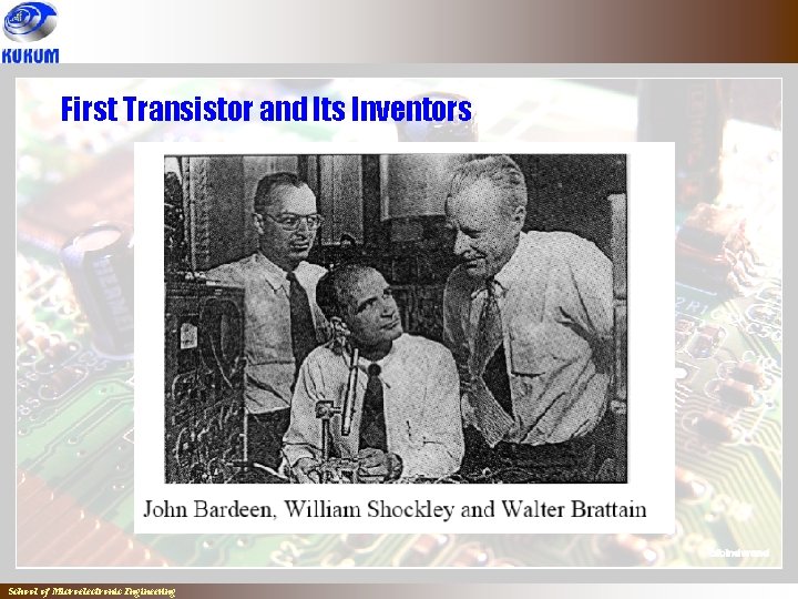
First Transistor, Bell Lab 1947 John Bardeen and Walter Brattain, demonstrated a solid state device made from germanium. They observed that when electrical signals were applied to contacts on germanium, the output power was larger than the input. These results were published In 1948. William Shockley, found out how the bipolar transistor functioned and published theory in 1949. Three of them shared the Nobel Prize in physics in 1956, School of Microelectronic Engineering

First Transistor and Its Inventors ` School of Microelectronic Engineering

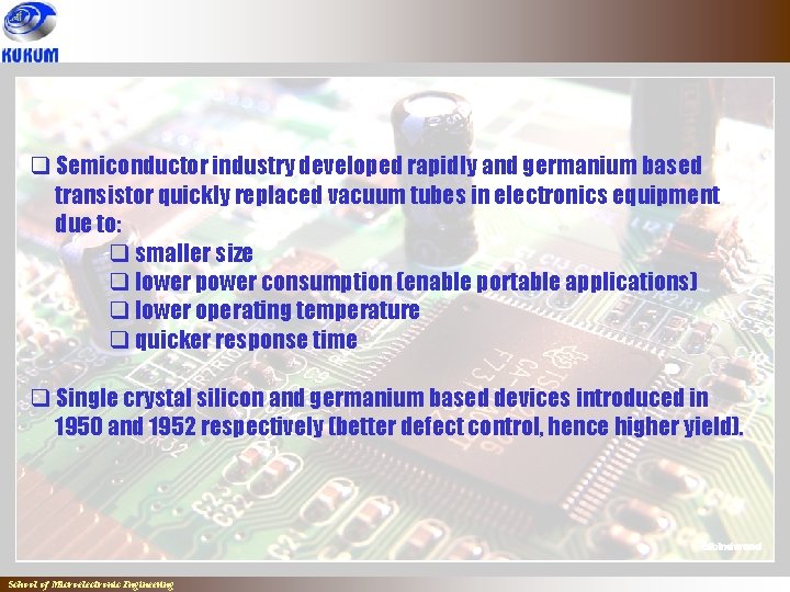
q Semiconductor industry developed rapidly and germanium based transistor quickly replaced vacuum tubes in electronics equipment due to: q smaller size q lower power consumption (enable portable applications) q lower operating temperature q quicker response time q Single crystal silicon and germanium based devices introduced in 1950 and 1952 respectively (better defect control, hence higher yield). School of Microelectronic Engineering

q Shockley left Bell Labs in 1956, to start his own lab in San Francisco Bay, California. Nowadays known as Silicon Valley. His lab has attracted talented scientist such as Robert Noyce and Gordon Moore. q Gordon Moore and Robert Noyce left Shockley in 1957 to start Fairchild Semiconductor. School of Microelectronic Engineering

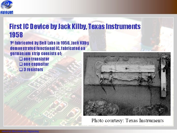
First IC Device by Jack Kilby, Texas Instruments 1958 1 st fabricated by Bell Labs in 1958. Jack Kilby demonstrated functional IC, fabricated on germanium strip consists of; q one transistor q one capacitor q 3 resistors ` School of Microelectronic Engineering

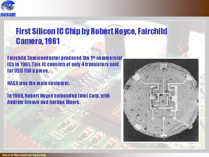
First Silicon IC Chip by Robert Noyce, Fairchild Camera, 1961 Fairchild Semiconductor produced the 1 st commercial ICs in 1961. This IC consists of only 4 transistors sold for USD 150 a piece. NASA was the main customer. In 1968, Robert Noyce cofounded Intel Corp. with Andrew Groove and Gordon Moore. School of Microelectronic Engineering

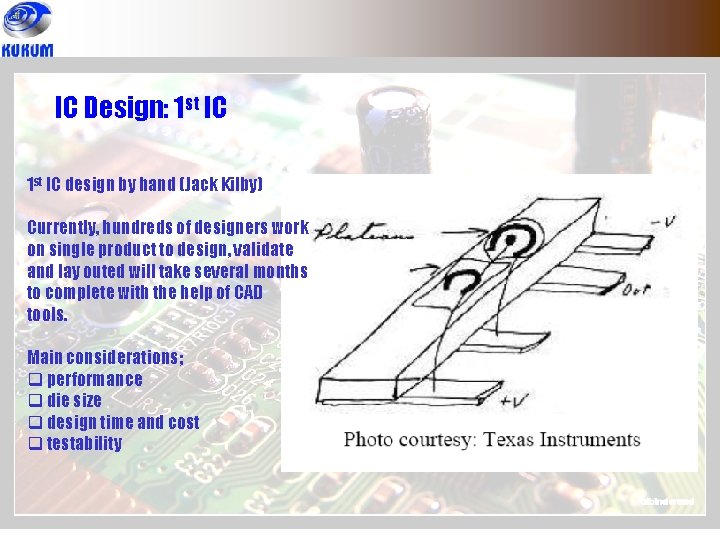
IC Design: 1 st IC design by hand (Jack Kilby) Currently, hundreds of designers work on single product to design, validate and lay outed will take several months to complete with the help of CAD tools. Main considerations; q performance q die size q design time and cost q testability `

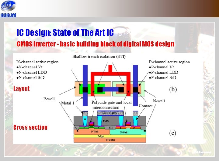
IC Design: State of The Art IC CMOS Inverter - basic building block of digital MOS design Layout Cross section

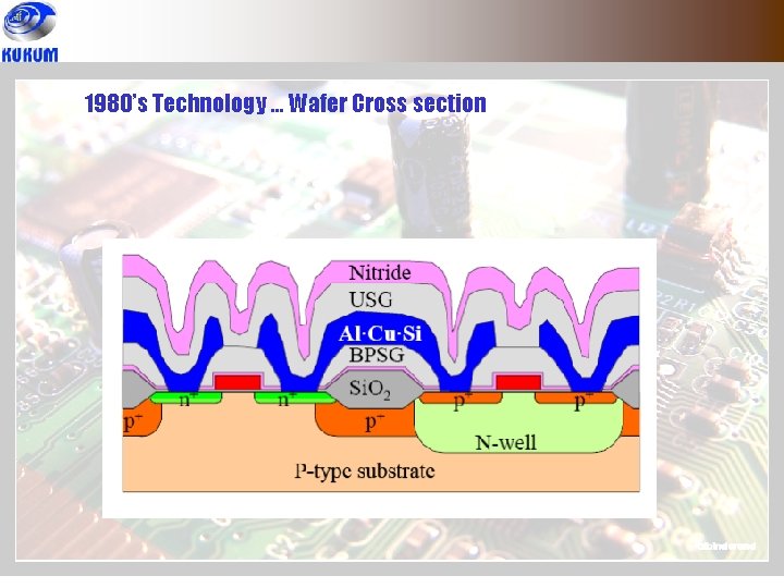
1980’s Technology … Wafer Cross section

1990’s Technology … Wafer Cross section

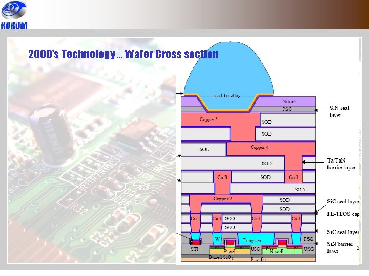
2000’s Technology … Wafer Cross section

Wafer Fabrication: From Design to Wafer ` School of Microelectronic Engineering

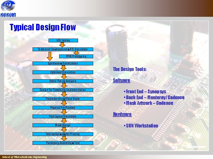
Typical Design Flow HDL Coding Testbench Development & RTL Simulation FPGA Prototyping Synthesis & Optimization Gatelevel Simulation Static Timing Analysis Design For Testability Implementation Floorplanning & Place Route Physical Verification Post Layout Simulation Mask Design Fabrication & Wafer Probing Packaging, Assembly & Test School of Microelectronic Engineering The Design Tools: Software • Front End – Synopsys • Back End – Monterey/Cadence • Mask Artwork – Cadence Hardware • SUN Workstation

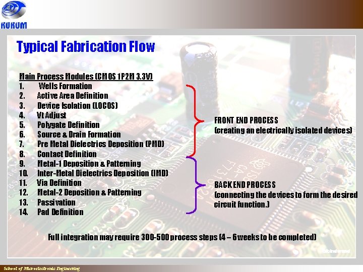
Typical Fabrication Flow Main Process Modules (CMOS 1 P 2 M 3. 3 V) 1. Wells Formation 2. Active Area Definition 3. Device Isolation (LOCOS) 4. Vt Adjust 5. Polygate Definition 6. Source & Drain Formation 7. Pre Metal Dielectrics Deposition (PMD) 8. Contact Definition 9. Metal-1 Deposition & Patterning 10. Inter-Metal Dielectrics Deposition (IMD) 11. Via Definition 12. Metal-2 Deposition & Patterning 13. Passivation 14. Pad Definition FRONT END PROCESS (creating an electrically isolated devices) BACK END PROCESS (connecting the devices to form the desired circuit function. ) Full integration may require 300 -500 process steps (4 – 6 weeks to be completed) School of Microelectronic Engineering

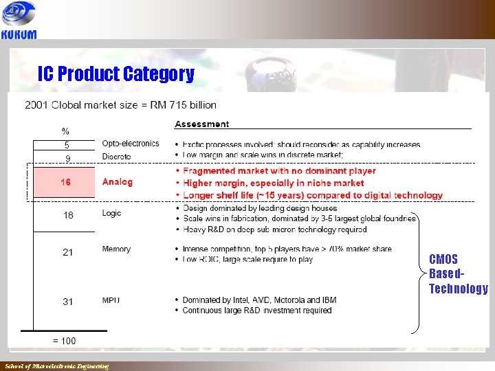
IC Product Category ` CMOS Based. Technology School of Microelectronic Engineering

Industry Structure School of Microelectronic Engineering

Semiconductor Manufacturing q A multi-dicipline processes, involved; q Circuit design q Manufacturing material q Clean room technology, processing, equipment q Wafer processing technology q Die testing q Chip packaging and final test School of Microelectronic Engineering

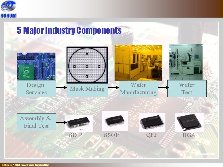
5 Major Industry Components Design Services Mask Making Wafer Manufacturing Wafer Test QFP BGA Assembly & Final Test SDIP School of Microelectronic Engineering SSOP

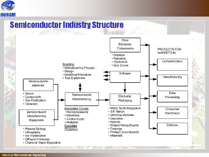
Semiconductor Industry Structure School of Microelectronic Engineering

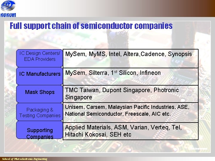
Full support chain of semiconductor companies IC Design Centers/ IC Design EDA Providers Centers/ EDA My. Sem, My. MS, Intel, Altera, Cadence, Synopsis Providers st IC IC Manufacturers My. Sem, Silterra, 1 Silicon, Infineon Mask Shops Packaging && Testing Companies Supporting Companies School of Microelectronic Engineering TMC Taiwan, Dupont Singapore, Photronic Singapore Unisem, Carsem, Malaysian Pacific Industries, ASE, National Semiconductor, Freescale, AIC etc. Applied Materials, ASM, Varian, Verteq, Tel, Hitachi Kokosai, SEH etc

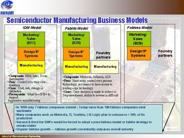
Semiconductor Manufacturing Business Models IDM Model Fablite Model Marketing/ Sales (B 2 C) Marketing/ Sales (B 2 B) Design/IP Systems Manufacturing • Companies: IBM, Intel, Texas Instruments • Pros: Control over their own roadmap • Cons: Cost, risk, swings in utilization • Prerequisite: Must be a $7 B+ to support Aggressive manufacturing. Fabless Model Marketing/ Sales (B 2 B) Foundry partners Design/IP Systems Manufacturing • Companies: Motorola, Infineon, ADI • Pros: Have some control over process technology, yet chance to have access to leading edge technology. • Cons: Once decision is made to reduce or Stop investment, ability to reverse is difficult. • In 1990 only 7 fabless companies existed ; Today more than 100 fabless companies exist worldwide • Many companies such as Motorola, TI, Tosibha, LSI Logic plan to outsource > 50% of its production • Second & third tier IDM’s would be forced to adopt a pure fabless model or fablite strategy to remain viable • Organic fabless growth — fabless growth consistently outpaces overall industry School of Microelectronic Engineering Foundry partners

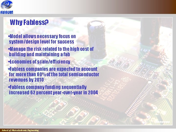
Why Fabless? • Model allows necessary focus on system/design level for success • Manage the risk related to the high cost of building and maintaining a fab • Economies of scale/efficiency • Fabless companies are expected to account for more than 60% of the total semiconductor revenues by 2010 • Fabless company funding sequentially increased 62 percent year-over-year in 2004 School of Microelectronic Engineering

Fabless Facts – Revenue Growth Semi Industry (in millions) The fabless sector has continuously achieved faster growth than the overall industry. Fabless (In millions) Source - FSA School of Microelectronic Engineering

Technology Trends & Challenges School of Microelectronic Engineering

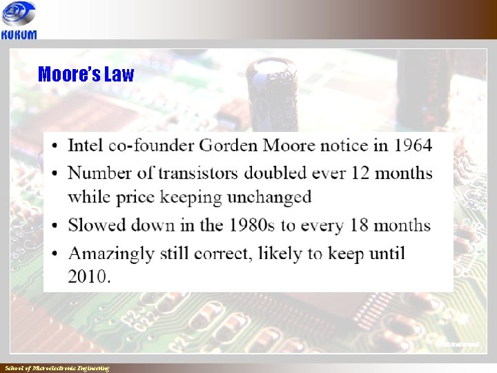
Moore’s Law ` School of Microelectronic Engineering

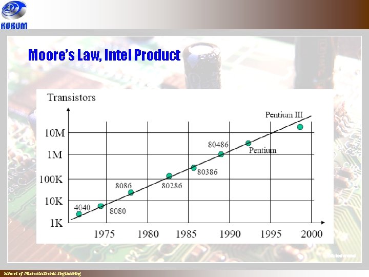
Moore’s Law, Intel Product ` School of Microelectronic Engineering

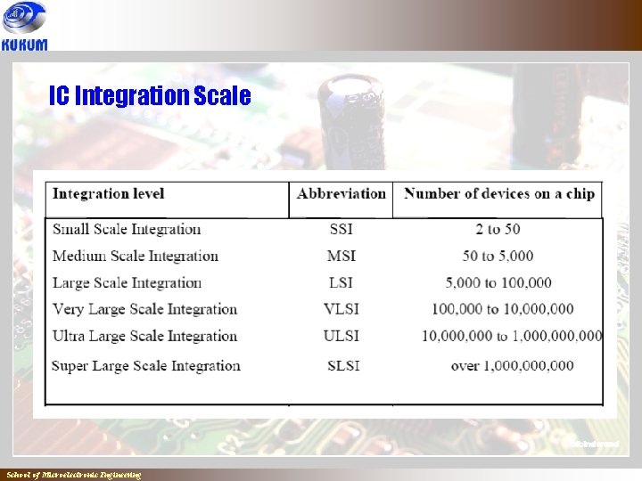
IC Integration Scale ` School of Microelectronic Engineering

Feature Size and Wafer Size ` School of Microelectronic Engineering

Road Map Semiconductor Industry ` School of Microelectronic Engineering

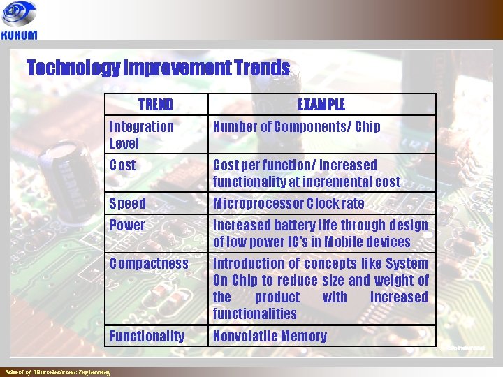
Technology Improvement Trends TREND EXAMPLE Integration Level Number of Components/ Chip Cost per function/ Increased functionality at incremental cost Speed Microprocessor Clock rate Power Increased battery life through design of low power IC’s in Mobile devices Compactness Introduction of concepts like System On Chip to reduce size and weight of the product with increased functionalities Functionality Nonvolatile Memory School of Microelectronic Engineering

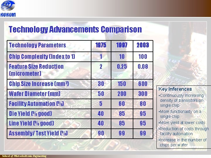
Technology Advancements Comparison Technology Parameters 1975 1997 2003 Chip Complexity (Index to 1) 1 10 100 Feature Size Reduction (micrometer) 2 0. 25 0. 08 Chip Size Increase (mm 2) 30 150 600 Wafer Diameter (mm) 50 200 300 Facility Automation (%) 5 60 80 Die Yield (% good) 40 85 95 Line Yield (% good) 40 85 95 Assembly/ Test Yield (%) 90 99 99 School of Microelectronic Engineering Key Inferences • Continuously increasing density of transistors on single chip • More functionality on a single chip • More yield at lower costs • Reduction of costs through facility automation • Increase in the number of chips per wafer

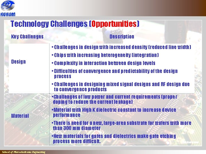
Technology Challenges (Opportunities) Key Challenges Description • Challenges in design with increased density (reduced line width) • Chips with increasing heterogeneity (integration) Design • Complexity in interaction between design levels • Difficulties of convergence and predictability of the design process • Challenges in designing mixed signal designs and RF design due to convergence products • Challenges of low power and current requirements (proper doping to reduce the current leakage) Material • Material with High K dielectric constant to increase device performance • There is need for a new, large-area substrate for wafers with more than 300 mm diameter • New materials for gates and dielectrics make gate etching process more difficult. School of Microelectronic Engineering

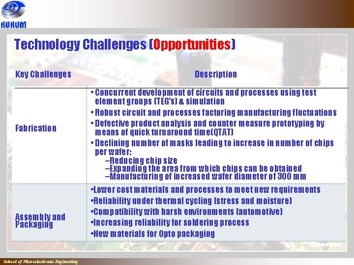
Technology Challenges (Opportunities) Key Challenges Fabrication Assembly and Packaging School of Microelectronic Engineering Description • Concurrent development of circuits and processes using test element groups (TEG’s) & simulation • Robust circuit and processes factoring manufacturing fluctuations • Defective product analysis and counter measure prototyping by means of quick turnaround time(QTAT) • Declining number of masks leading to increase in number of chips per wafer: –Reducing chip size –Expanding the area from which chips can be obtained –Manufacturing of increased wafer diameter of 300 mm • Lower cost materials and processes to meet new requirements • Reliability under thermal cycling (stress and moisture) • Compatibility with harsh environments (automotive) • Increasing reliability for soldering process • New materials for Opto packaging

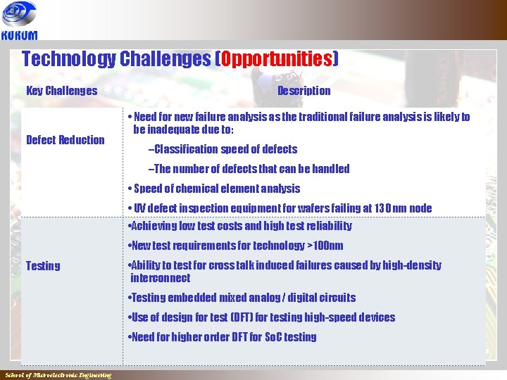
Technology Challenges (Opportunities) Key Challenges Defect Reduction Description • Need for new failure analysis as the traditional failure analysis is likely to be inadequate due to: –Classification speed of defects –The number of defects that can be handled • Speed of chemical element analysis • UV defect inspection equipment for wafers failing at 130 nm node • Achieving low test costs and high test reliability • New test requirements for technology >100 nm Testing • Ability to test for cross talk induced failures caused by high-density interconnect • Testing embedded mixed analog/ digital circuits • Use of design for test (DFT) for testing high-speed devices • Need for higher order DFT for So. C testing School of Microelectronic Engineering

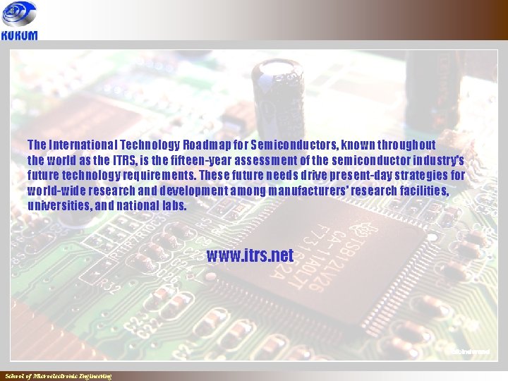
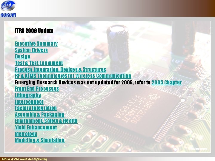
The International Technology Roadmap for Semiconductors, known throughout the world as the ITRS, is the fifteen-year assessment of the semiconductor industry’s future technology requirements. These future needs drive present-day strategies for world-wide research and development among manufacturers’ research facilities, universities, and national labs. www. itrs. net School of Microelectronic Engineering

ITRS 2006 Update Executive Summary System Drivers Design Test & Test Equipment Process Integration, Devices & Structures RF & A/MS Technologies for Wireless Communication Emerging Research Devices was not updated for 2006, refer to 2005 Chapter Front End Processes Lithography Interconnect Factory Integration Assembly & Packaging Environment, Safety & Health Yield Enhancement Metrology Modeling & Simulation School of Microelectronic Engineering

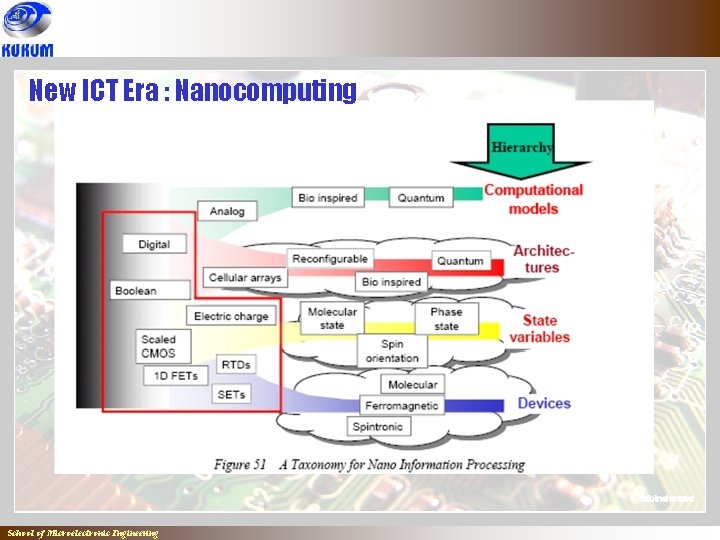
New ICT Era : Nanocomputing School of Microelectronic Engineering

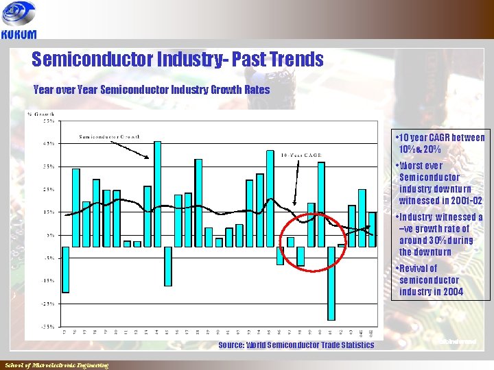
Semiconductor Industry- Past Trends Year over Year Semiconductor Industry Growth Rates • 10 year CAGR between 10% & 20% • Worst ever Semiconductor industry downturn witnessed in 2001 -02 • Industry witnessed a –ve growth rate of around 30% during the downturn • Revival of semiconductor industry in 2004 Source: World Semiconductor Trade Statistics School of Microelectronic Engineering

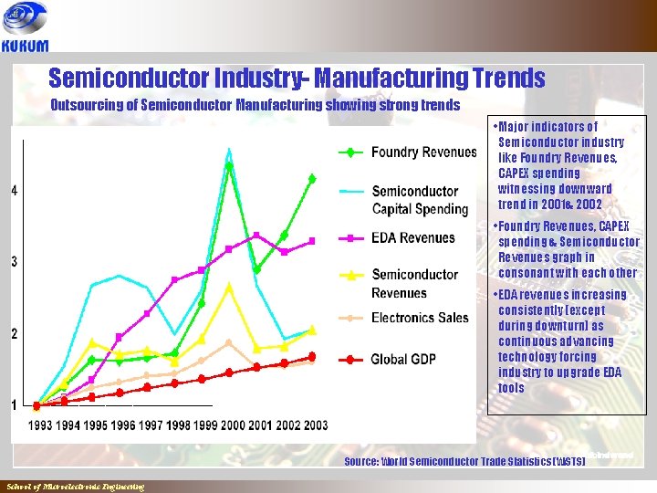
Semiconductor Industry- Manufacturing Trends Outsourcing of Semiconductor Manufacturing showing strong trends • Major indicators of Semiconductor industry like Foundry Revenues, CAPEX spending witnessing downward trend in 2001& 2002 • Foundry Revenues, CAPEX spending & Semiconductor Revenues graph in consonant with each other • EDA revenues increasing consistently (except during downturn) as continuous advancing technology forcing industry to upgrade EDA tools Source: World Semiconductor Trade Statistics (WSTS) School of Microelectronic Engineering

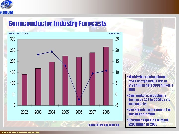
Semiconductor Industry Forecasts Revenues in $ Billion Growth Rate • World wide semiconductor revenue expected to rise to $199 billion from $166 billion in 2003 • Chip market is expected to decline by 2. 3%in 2006 due to overcapacity • New growth cycle expected to commence in 2007 Source: Frost and Sullivan School of Microelectronic Engineering • Revenues expected to reach $266 billion by 2008

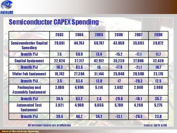
Semiconductor CAPEX Spending 2003 2004 2005 2006 2007 2008 Semiconductor Capital Spending 29, 661 44, 763 50, 767 43, 058 35, 693 39, 872 Growth (%) 7. 5 50. 9 13. 4 -15. 2 -17. 1 11. 7 Capital Equipment 22, 824 37, 317 42, 912 35, 230 27, 806 32, 439 Growth (%) 10. 3 63. 5 15 -17. 9 -21. 1 16. 7 Wafer Fab Equipment 16, 742 27, 364 31, 144 25, 848 20, 598 23, 176 Growth (%) 3. 5 63. 4 13. 8 -17 -20. 3 12. 5 Packaging and Assembly Equipment 3, 060 4, 994 5, 114 3, 602 2, 949 3, 988 Growth (%) 30. 5 63. 2 2. 4 -29. 6 -18. 1 35. 2 Automated Test Equipment 3, 021 4, 960 6, 655 5, 780 4, 260 5, 275 Growth (%) 39. 4 64. 2 34. 2 -13. 1 -26. 3 23. 8 All Revenue Figures are in $Millions School of Microelectronic Engineering Source: WSTS & SIA

Semiconductor Industry in Malaysia School of Microelectronic Engineering

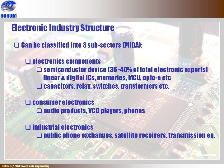
Electronic Industry Structure q Can be classified into 3 sub-sectors (MIDA); q electronics components q semiconductor device (35 -40% of total electronic exports) linear & digital ICs, memories, MCU, opto-e etc q capacitors, relay, switches, transformers etc. q consumer electronics q audio products, VCD players, phones q industrial electronics q public phone exchanges, satellite receivers, transmission eq. School of Microelectronic Engineering

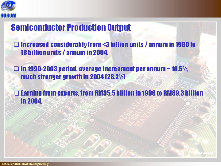
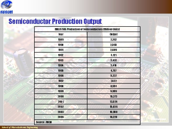
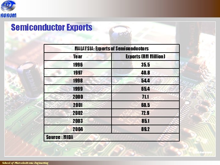
Semiconductor Production Output q Increased considerably from <3 billion units / annum in 1980 to 18 billion units / annum in 2004. q In 1990 -2003 period, average increament per annum ~ 16. 5%, much stronger growth in 2004 (28. 2%) q Earning from exports, from RM 35. 5 billion in 1996 to RM 89. 3 billion in 2004. School of Microelectronic Engineering

Semiconductor Production Output MALAYSIA: Production of Semiconductors (Million Units) Source : MIDA School of Microelectronic Engineering Year Output 1989 2, 262 1990 2, 565 1991 2, 689 1992 3, 121 1993 3, 491 1994 3, 410 1995 4, 757 1996 5, 237 1997 7, 432 1998 8, 951 1999 9, 959 2000 16, 373 2001 13, 524 2002 15, 036 2003 15, 958 2004 18, 228

Semiconductor Exports MALAYSIA: Exports of Semiconductors Year Exports (RM Million) 1996 35. 5 1997 40. 8 1998 54. 4 1999 65. 4 2000 71. 1 2001 60. 5 2002 72. 9 2003 85. 1 2004 89. 2 Source : MIDA School of Microelectronic Engineering

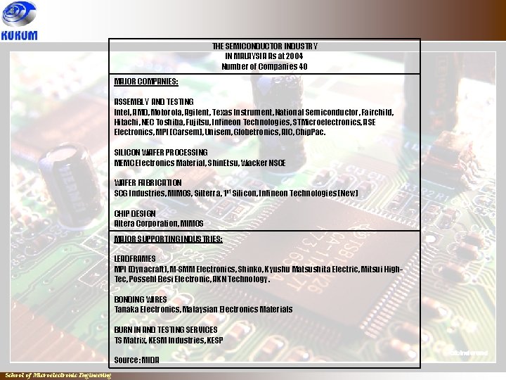
THE SEMICONDUCTOR INDUSTRY IN MALAYSIA As at 2004 Number of Companies 40 MAJOR COMPANIES: ASSEMBLY AND TESTING Intel, AMD, Motorola, Agilent, Texas Instrument, National Semiconductor, Fairchild, Hitachi, NEC Toshiba, Fujitsu, Infineon Technologies, STMicroelectronics, ASE Electronics, MPI (Carsem), Unisem, Globetronics, AIC, Chip. Pac. SILICON WAFER PROCESSING MEMC Electronics Material, Shin. Etsu, Wacker NSCE WAFER FABRICATION SCG Industries, MIMOS, Silterra, 1 st Silicon, Infineon Technologies (New) CHIP DESIGN Altera Corporation, MIMOS MAJOR SUPPORTING INDUSTRIES: LEADFRAMES MPI (Dynacraft), M-SMM Electronics, Shinko, Kyushu Matsushita Electric, Mitsui High. Tec, Possehl Besi Electronic, AKN Technology. BONDING WIRES Tanaka Electronics, Malaysian Electronics Materials BURN IN AND TESTING SERVICES TS Matrix, KESM Industries, KESP Source: MIDA School of Microelectronic Engineering

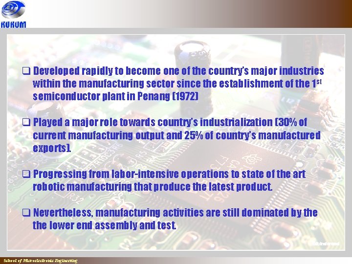
q Developed rapidly to become one of the country’s major industries within the manufacturing sector since the establishment of the 1 st semiconductor plant in Penang (1972) q Played a major role towards country’s industrialization (30% of current manufacturing output and 25% of country’s manufactured exports). q Progressing from labor-intensive operations to state of the art robotic manufacturing that produce the latest product. q Nevertheless, manufacturing activities are still dominated by the lower end assembly and test. School of Microelectronic Engineering

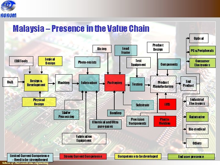
Malaysia – Presence in the Value Chain Optical Logical Design EDA Tools R&D Design & Development Test Equipment Photo-resists Masking Fabrication Product Design Lead Frame Dicing Packaging Physical Design Testing Product Manufacturing Precision Components Fabrication Equipment Limited Current Competence – Need to be strengthened School of Microelectronic Engineering EMS Bonding Chemical and Ultra pure gases Strong Current Competence Consumer Electronics Components Substrate Wafer Processing PC & Peripherals Plastic Molding End Product Industrial Electronics Automotive Bio-medical Others Competence to be developed End user presence

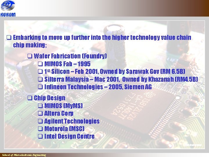
q Embarking to move up further into the higher technology value chain chip making; q Wafer Fabrication (Foundry) q MIMOS Fab – 1995 q 1 st Silicon – Feb 2001, Owned by Sarawak Gov (RM 6. 5 B) q Silterra Malaysia – Mac 2001, Owned by Khazanah (RM 4. 5 B) q Infineon Technologies – 2005, Siemen AG q Chip Design q MIMOS (My. MS) q Altera Corp q Agilent Technologies q Motorola (MSC) q Intel Design Centre School of Microelectronic Engineering

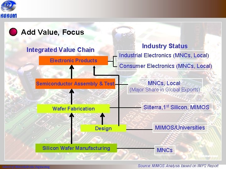
Add Value, Focus Industry Status Integrated Value Chain Electronic Products Semiconductor Assembly & Test Industrial Electronics (MNCs, Local) Consumer Electronics (MNCs, Local) MNCs, Local (Major Share in Global Exports) Silterra, 1 st Silicon, MIMOS Wafer Fabrication Design Silicon Wafer Manufacturing School of Microelectronic Engineering MIMOS/Universities MNCs Source: MIMOS Analysis based on IMP 2 Report

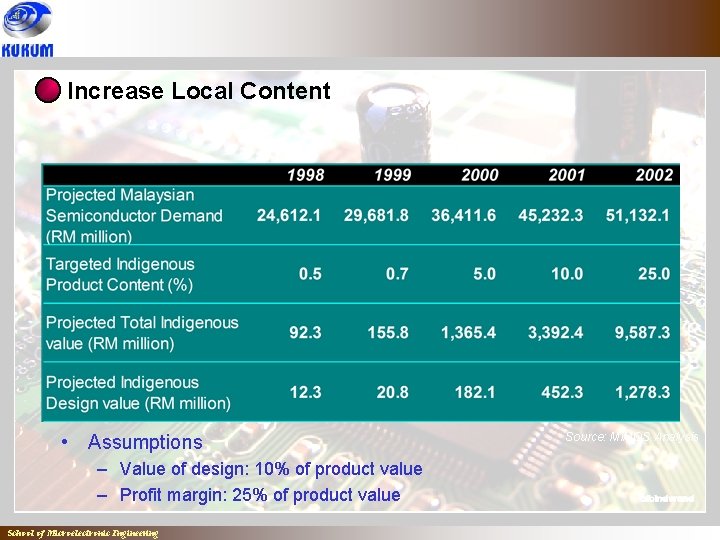
Increase Local Content • Assumptions – Value of design: 10% of product value – Profit margin: 25% of product value School of Microelectronic Engineering Source: MIMOS Analysis

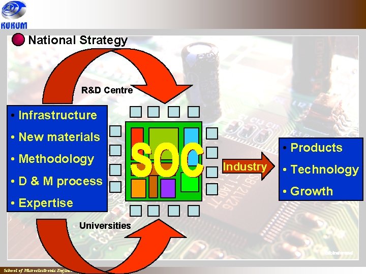
National Strategy R&D Centre • Infrastructure • New materials • Methodology • D & M process • Expertise Universities School of Microelectronic Engineering • Products Industry • Technology • Growth

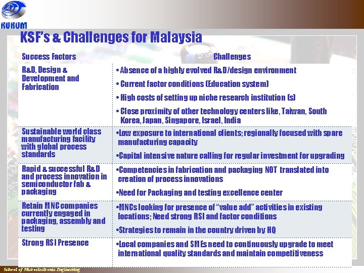
KSF’s & Challenges for Malaysia Success Factors R&D, Design & Development and Fabrication Challenges • Absence of a highly evolved R&D/design environment • Current factor conditions (Education system) • High costs of setting up niche research institution (s) • Close proximity of other technology centers like, Taiwan, South Korea, Japan, Singapore, Israel, India Sustainable world class manufacturing facility with global process standards • Low exposure to international clients; regionally focused with spare manufacturing capacity Rapid & successful R&D and process innovation in semiconductor fab & packaging • Competencies in fabrication and packaging NOT translated into creation of process innovations Retain MNC companies currently engaged in packaging, assembly and testing • MNCs looking for presence of “value add” activities in existing locations; Need strong RSI and factor conditions Strong RSI Presence • Local companies and SMEs need to continuously upgrade to meet international quality standards and maintain competitiveness School of Microelectronic Engineering • Capital intensive nature calling for regular investment for upgrading • Need for Packaging and testing excellence center • Strategies to remain in the country driven by HQ

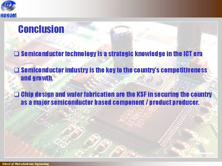
Conclusion q Semiconductor technology is a strategic knowledge in the ICT era q Semiconductor industry is the key to the country’s competitiveness and growth. q Chip design and wafer fabrication are the KSF in securing the country as a major semiconductor based component / product producer. School of Microelectronic Engineering