Intrinsic Semiconductor A Semiconductor which does not have


, Arsenic (As)")


 Vd=µE Where E is applied field and µ= mobility of charge")


 For intrinsic Ge, ne= nh= ni where ne= concentration of electrons, nh=")
![Now put value of q, µe , µh, σ in equation [2], then](https://slidetodoc.com/presentation_image_h/96747d9937ec02434e6710b5b891dc13/image-19.jpg "Now put value of q, µe , µh, σ in equation [2], then")
![By solving eq. [3] and eq. [4], we have ne = 3. 88*](https://slidetodoc.com/presentation_image_h/96747d9937ec02434e6710b5b891dc13/image-20.jpg "By solving eq. [3] and eq. [4], we have ne = 3. 88*")


 = 2. 5 × 10¹⁹/m 3 Mobility")

 = 1. 5 × 10¹⁶/m 3 Mobility of electrons (μe)")


 resistance that changes with the")


 by (i) (ii) 2 mc 2 h k")


 by (ii) d dv. dv dk 2 mov 2 mo d v")


 now becomes This is the time independent (steady state) Schrodinger’s wave equation")
 Schrodinger’s wave equation for a particle")
- Slides: 97
Intrinsic Semiconductor Ø A Semiconductor which does not have any kind of impurities, behaves as an Insulator at 00 K and behaves as a Conductor at higher temperature is known as Intrinsic Semiconductor or Pure Semiconductors. Ø Germanium and Silicon are the best examples of intrinsic semiconductors.
Energy Band Structure for Intrinsic Semiconductors
Extrinsic Semiconductors Ø
N - type Semiconductors Ø When any pentavalent element such as Phosphorous(P), Arsenic (As) or Antimony(Sb) is added to an intrinsic Semiconductor , 4 electrons are involved in covalent bonding with 4 neighboring pure Semiconductor atoms. Ø The fifth electron is weakly bound to the parent atom and even for lesser thermal energy it is released leaving the parent atom positively ionized.
N - type Semiconductors Ø The Intrinsic Semiconductors doped with pentavalent impurities are called N-type Semiconductors. Ø The energy level of fifth electron is called donor level. Ø The donor level is close to the bottom of the conduction band. Most of the donor level electrons are excited in to the conduction band at room temperature and become the Majority charge carriers. Ø Hence in N-type Semiconductors electrons are majority carriers and holes are minority carriers.
Energy Band Structure for N-Type Semiconductors
P - type Semiconductors Ø When a trivalent elements such as Al, Ga or In added to the Intrinsic Semiconductor, all the three electrons of these are involved in Covalent bonding with the three neighboring Si atoms. Ø These type of trivalent impurities are called acceptor impurities and the semiconductors doped with the acceptor impurities are called P-type Semiconductors. Ø Even at relatively low temperatures, these acceptor atoms get ionized taking electrons from valence band thus giving rise to holes in valence band for conduction.
P - type Semiconductors Ø Due to ionization of acceptor atoms only holes are created and there is no creation of electrons. Ø Thus holes are more in number than electrons and hence holes are majority carriers and electros are minority carriers in P-type semiconductors.
Energy Band Structure for P-Type Semiconductors
Carrier drift Electron and holes will move under the influence of an applied electric field since the field exert a force on charge carriers (electrons and holes). F = q. E These movements result a current of Id Id = nq A Vd where Id = drift current n= number of charge carriers per unit volume Vd = drift velocity of charge carrier q= charge of the electron A= area of the semiconductor
Carrier Mobility (µ) Vd=µE Where E is applied field and µ= mobility of charge carrier which is a proportionality factor µ = Vd / E (cm 2 / V-sec) so µ is a measure how easily charge carriers move under the influence of an applied field or µ determines how mobile the charge carriers are.
n- type Si Current carriers are mostly electrons
p- type Si Current carriers are mostly holes
How long does a carrier move in time before collision? The average time taken between collisions is called as relaxation time, (or mean free time) How far does a carrier move in space (distance) before a collision? The average distance taken between collisions is called as mean free path,
Mobility of holes is lower than electrons. Mobility is also related to mean free time by following relation Where m is mass of electron (9. 1 * 10 -31 kg. )
Conductivity is Current carrying capacity of a material. Current density is given by J = nq. V = nqµE = σE This equation is recognized as ohm’s law, namely the conduction current is proportional to the applied voltage. The energy which the electron acquire from the applied field is, as a result of collisions, given to the lattice ions. Hence power is dissipated within the metal by the electrons, and the power density is given by J. E =σ E 2(watts per cubic meter) Conductivity σ = nqµ is the conductivity of the metal in (ohm-meter)-1
Numerical Q. 1 A sample of Ge is doped to the extent of 1014 donor atoms/cm 3 and 7*1013 acceptor atoms /cm 3. At temperature of the sample the resistivity of pure(intrinsic) Ge is 60 Ω- cm. If the applied voltage is 2 V/cm , find the total conduction current density. Here mobility of electron = 3800 cm 2 /V-sec & Mobility of holes = 1800 cm 2 /V-sec.
Solution: i) For intrinsic Ge, ne= nh= ni where ne= concentration of electrons, nh= concentration of holes, ni= intrinsic concentration and conductivity σ = ni q(µe + µh) ……. . eq. [1] where µe= mobility of electrons and µh = mobility of holes by rearranging eq. [1] ni= σ/ q(µe + µh) ……. . . eq. [2] Since conductivity is also given by σ = 1/ ρ where ρ is resistivity which is given in question. So σ = 1/60 (Ω-cm)-1
Now put value of q, µe , µh, σ in equation [2], then ni = 1. 86* 1013/cm 3 According to Mass Action Law ne * nh= ni 2 ne * nh = (1. 86* 1013)2 = 3. 45*1026 ……. eq. [3] Semiconductor is electrically neutral, so Nd + nh = Na + ne ne - nh= Nd – Na = 1014 - 7*1013 ne - nh = 3*1013 ……eq. [4]
By solving eq. [3] and eq. [4], we have ne = 3. 88* 1013 / cm 3 and nh = 0. 88* 1013 / cm 3 As we know, current density J = σE J = (neµe + nhµh ) q E Where E is electric field By putting values of ne, µe, nh, µh, q, E J= 52. 24 m. A/cm 2
Resistivity The electrical resistivity of a particular conductor material is a measure of how strongly the material opposes the flow of electric current through it. Where: R is the resistance in ohms (Ω), L is the length in metres (m), A is the area in square metres (m 2), and where the proportional constant ρ (the Greek letter “rho”) is known as Resistivity in Ωm.
Conductivity and Resistivity relation Unit of conductivity is mho or Ωm-1 Materials such as copper and aluminium are known for their low levels of resistivity thus allowing electrical current to easily flow through them making these materials ideal for making electrical wires and cables. Silver and gold have much low resistivity values, but for obvious reasons are more expensive to turn into electrical wires.
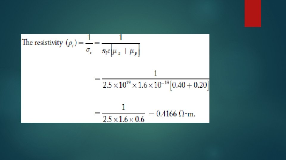
Numerical Q. Find the resistivity of an intrinsic semiconductor with intrinsic concentration of 2. 5 × 10¹⁹ per m 3. The mobilities of electrons and holes are 0. 40 m 2/ V-s and 0. 20 m 2/ V-s.
Solution: Given data are: Intrinsic concentration (ni) = 2. 5 × 10¹⁹/m 3 Mobility of electrons (μn) = 0. 40 m 2/V-s The mobility of holes (μp) = 0. 20 m 2/V-s Now since the conductivity of an intrinsic semiconductor (σi) = nie[μn + μp]
Q. Find the conductivity of intrinsic silicon at 300 K. It is given that ni at 300 K in silicon is 1. 5 × 10¹⁶/m 3 and the mobilities of electrons and holes in silicon are 0. 13 m 2/V-s and 0. 05 m 2/V-s, respectively
Solution: Intrinsic concentration (ni) = 1. 5 × 10¹⁶/m 3 Mobility of electrons (μe) = 0. 13 m 2/V-m Mobility of holes (μh) = 0. 05 m 2/V-m Conductivity (σ) = nie (μe + μh) = 1. 5 × 1016 × 10− 19 (0. 13 + 0. 05)/Ω-m = 4. 32 × 10− 4/Ω-m
Q. Calculate the number of donor atoms per m 3 of n-type material having resistivity of 0. 25 Ω-m, the mobility of electrons is 0. 3 m 2/V-s.
Solution: We know [Since n is number of free electron per m 3 ≈ number of donor atoms in n-type]
What are the Drift Current and Diffusion Current? In a semiconductor material, the drift, as well as diffusion currents, will occur. Semiconductors are fabricated with two kinds of materials namely p- type as well as n-type. There are several kinds of switching devices available like transistors, diodes, etc. which are designed by placing one material among other materials so that the material’s conducting property can be modified.
What is a Drift Current? Drift current can be defined as the charge carrier’s moves in a semiconductor because of the electric field. There are two kinds of charge carriers in a semiconductor like holes and electrons. Once the voltage is applied to a semiconductor, then electrons move toward the +ve terminal of a battery whereas the holes travel toward the –ve terminal of a battery. J = µnq. E Unit of J is amperes per square meter.
What is Diffusion Current? The diffusion current can be defined as the flow of charge carriers within a semiconductor travels from a higher concentration region to a lower concentration region. A higher concentration region is nothing but where the more number of electrons present in the semiconductor. Similarly, a lower concentration region is where the less number of electrons present in the semiconductor. The process of diffusion mainly occurs when a semiconductor is doped non-uniformly.
What is Diffusion Current? In an N-type semiconductor, when it is doped non-uniformly then a higher concentration region can be formed at the left side whereas the lower concentration region can be formed at the right side. The electrons in the higher concentration region are more in the semiconductor so they will experience a repulsive force from each other.
Difference between Drift Current and Diffusion Currents S. No. Drift Current Diffusion Current 1. The movement of charge carriers is because of the applied electric field is known as drift current 2 It requires electrical energy for the process Some amount of external energy is enough of drift current for the process of diffusion current 3 This current obeys Ohm’s Law This current obeys Fick’s Law. 4. The direction of charge carriers in the semiconductor is reverse to each other. For charge carriers, the densities of diffusion are reverse in symbol to each other The diffusion current can be occurred because of the diffusion in charge carriers
Difference between Drift Current and Diffusion Currents S. No. Drift Current Diffusion Current 5. The direction of the drift current, as well as the electric field, will be the same The direction of this current can be decided by the concentration of the carrier slope 6. It depends on the permittivity It is independent of permittivity 7. The direction of this current mainly depends on the polarity of the applied electric field The direction of this current mainly depends on the charge within the concentrations of carrier
Einstein Relationship Since both diffusion and mobility are statistical thermodynamic phenomena, D and µ are not independent. The relationship between them is given by the Einstein equation where VT is the “volt-equivalent of temperature, ” defined by where k is the Boltzmann constant in joules per degree Kelvin given by 1. 60 X 1019 k
where k is the Boltzmann constant in joules per degree Kelvin k is given by 1. 60 X 1019 k At room temperature (300 K) VT = 0. 026 Y, µ = 39 D.
Numerical Q. At 300 K, find the diffusion coefficient of electrons in silicon. Given the mobility of electrons (μn) is 0. 21 m 2/V-s.
Solution: From Einstein’s equation, we know
Sheet Resistance When the wafer is doped, the conductivity of the material increases. The level of doping can be estimated by measuring the conductivity. Consider two metal lines of same depth (D), but with different width and lengths. Schematic of two lines with the same depth, but different lengths and widths
The resistance of the first and second metal line is given by ……. Eq. 3 where ρ is the resistivity of the material. Since the depth is the same for both lines, the resistance is proportional to the ratio of length to width. The ratio of resistivity to depth is called “sheet resistance” Rs = ρ/D ……… Eq. 4 Rs is sheet Resitance
By putting Eq. -4 into Eq. - 3 R 1 =RS L 1/W 1 and R 2 =RS L 2/W 2 For a given layer (i. e. when the material and the depth are fixed), the sheet resistance is a constant and is expressed as ‘ohm/square’ or sometimes written as “ohm/□’.
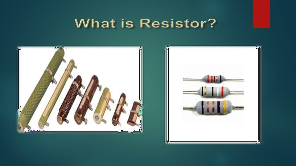
A resistor is a passive electronic component that we use in electronic circuits either to limit current through an active component or to reduce voltage in the circuit (by dropping voltage across the resistor ). Current through a resistor is directly proportional to the voltage applied across the resistor. This is derived from Ohms Law and is represented by equation I = V/R, where I=current through resistor (in amperes), V = voltage across resistor (in volts) and R = resistance (in ohms)
1. 2. 3. 4. 5. 6. 7. Fixed Resistor Variable Resistor Rheostat Tapped Resistor Thermistor Light Dependent Resistor (LDR) Voltage Dependent Resistor
1. Fixed Resistor: A fixed resistor cannot be changed as it is set at a specific value.
Carbon composition type resistor This is the most common type of low wattage resistor. The resistive material is of carbon-clay composition and the leads are made of tinned copper. These resistors are cheap and reliable and stability is high.
Wire wound resistors: Ø Ø Ø These resistors are a length of wire wound an insulating cylindrical core. Usually wires of material such as constantan (60% copper and 40% nickel) and manganin which have high resistivity and low temperature coefficients are employed. The completed wire wound resistor is coated with an insulating material such as baked enamel.
Metalized resistors It is constructed using film deposition techniques of depositing a thick film of resistive material onto an insulating substrate. Only approximate values of resistance can be had by this method.
2. Variable resistor Øa device that is used to change the resistance according to our needs in an electronic circuit. ØIt can be used as a three terminal as well as a two terminal device. ØMostly they are used as a three terminal device. Variable resistors are mostly used for device calibration.
Variable resistor symbol for circuit diagrams Variable resistor element with two connections
Variable resistor variable resistor symbol used in circuit diagrams indicates its construction. Effectively it is a fixed resistor with a slider that can move along the length of the resistive element. In this way it forms a potentiometer. It depicts the current version use in circuit diagrams today and the traditional format that may be seen on older circuit diagrams
Variable resistor variable resistor symbol used in circuit diagrams indicates its construction. Effectively it is a fixed resistor with a slider that can move along the length of the resistive element. In this way it forms a potentiometer as described before. It depicts the current version use in circuit diagrams today and the traditional format that may be seen on older circuit diagrams
Two main disadvantages with the wire wound variable resistor: The first is that often as the slider moves over the wires, the resistance changes have discrete steps. This may not be a problem in many applications, but it is a point to note. The second is that they are not suitable even for low frequency RF applications as the resistance wire forms a coil and has significant inductance.
Cermet variable resistors are widely used, particularly for trimmer resistors. The name cermet is derived from the fact that the resistive element is made from CERamic and METal. The resistive element is made from a mixture of fine metal oxides or precious metal particles and glass in a viscous organic material. The resulting paste is applied to the substrate and fired to solidify the mixture. Cermet variable resistors are ideal for trimmer resistors because they have a low to medium adjustment life, and they often have temperature coefficients of around ± 100 ppm/°C.
Carbon composition variable resistors For the carbon composition variable resistor, a mixture of carbon powder and a binder are molded under heat into the required shape. In some manufacturing processes the carbon composition element is molded at the same time as the plastic substrate. Carbon composition variable resistors are some of the least expensive types and they are widely used in many areas. they are a good all round general purpose variable resistor.
3. Rheostat It is an adjustable or variable resistor. It is used to control the electrical resistance of a circuit without interrupting the flow of current. Rheostat has 3 terminals and usually consist of a resistive wire wrapped to form a toroid coil with a wiper that slides along the surface of the coil. It is most often designed with a ceramic core. Rheostats are used in applications that require high voltage and current.
As a result of the reduction of size and power consumption in many of today’s electrical devices rheostats, once are very common item in commercial and industrial products, have been replaced by potentiometers. The most common uses today for rheostats are as light dimmers and motor speed controls. They are often used in arc lamps, pumps, fans and blowers, respirators, dental and medical equipment and model trains.
Tapped Resistor
4. Tapped Resistor A wire wound fixed resistor having one or more additional terminals along its length, generally for voltage-divider applications
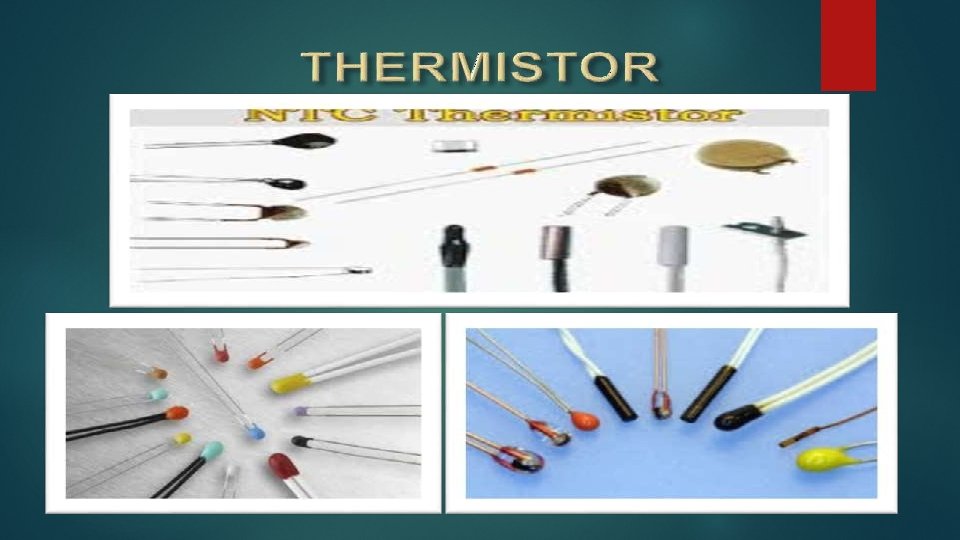
5. Thermistor -is a thermally sensitive resistor whose resistance value changes with changes in operating temperature. Because of the self- heating effect of current in a thermistor, the device changes resistance with changes in current. It exhibits either a positive temperature coefficient (PTC) or a negative temperature coefficient (NTC).
If a thermistor has a positive temperature coefficient, its resistance increases as the operating temperature increases. Conversely, if a thermistor has a negative temperature coefficient, its resistance decreases as the operating temperature increases. Thermistors are frequently used in electronic circuits that handle temperature measurement, temperature control, and temperature compensation. In digital thermometers, it is used to measure oil and coolant temperatures, and also used in ovens and refrigerators, but they are also found in almost any application that requires heating or cooling protection circuits for safe operation.
Thermistor symbols The arrow by the T signifies that the resistance is variable based on temperature. The direction of the arrow or bar is not significant.
How does thermistor "read" temperature? A thermistor does not actually "read" anything, instead the resistance of a thermistor changes with temperature. How much the resistance changes depends on the type of material used in thermistor
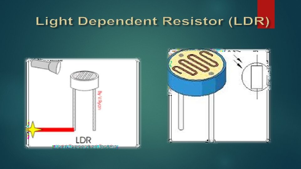
An LDR is a component that has a (variable) resistance that changes with the light intensity that falls upon it. This allows them to be used in light sensing circuits. Hence, they are light sensitive devices. They are also called as photo conductors, photo conductive cells or simply photocells. They are made up of semiconductor materials having high resistance.
There are many different symbols used to indicate a LDR, one of the most commonly used symbol is shown in the figure below. The arrow indicates light falling on it.
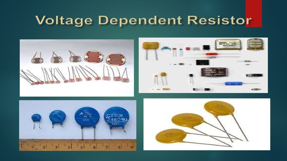
Varistor are voltage dependent, nonlinear device which have an electrical behavior similar to back-to-back zener diodes. It provide reliable and economical protection against high voltage transients and surges which may be produced, for example, by lighting, switching or electrical noise on AC or DC power lines. They have the advantage over transient suppressor diodes in as much as they can absorb much higher transient energies and can suppress positive and negative transients.
When a transient occurs, the varistor resistance changes from a very high stand-by value to a very low conducting value. The transient is thus absorbed and clamped to a safe level, protecting sensitive circuit components. Varistor are manufactured from a non-homogeneous material, giving a rectifying action at the contact points of two particles. Many series and parallel connections determine the voltage rating and the current capability of the varistor
Quantum Mechanics
E-K Diagram Ø Ø • • • An E-k diagram shows characteristics of a particular semiconductor material. It shows the relationship between the energy and momentum of available quantum mechanical states for electrons in the material. x-axis can be either momentum or wavenumber and y-axis is energy. E-k diagram shows: The band gap (EG), which is the difference in energy between the top of the valence band the bottom of the conduction band. The effective mass of electrons and holes in the material. This is given by the curvature of each of the bands. This diagram indicates how the actual electron states are equally spaced in k-space. Which means that the density of states in E depends on the slope of the E-k curve.
E-K Diagram
Introduction There a few phenomenon which the classical mechanics failed to explain. 1. Stability of an atom 2. Spectral series of Hydrogen atom 3. Black body radiation Max Planck in 1900 at a meeting of German Physical Society read his paper “On theory of the Energy distribution law of the Normal Spectrum”. This was the start of the revolution of Physics i. e. the start of Quantum Mechanics.
Quantum Mechanics Ø It is a generalization of Classical Physics that includes classical laws as special cases. Ø Quantum Physics extends that range to the region of small dimensions. Ø Just as ‘c’ the velocity of light signifies universal constant, the Planck's constant characterizes Quantum Physics. h = 6. 65 X 10 -27 erg. sec h = 6. 625 X 10 -34 Joule. sec
Quantum Mechanics It is able to explain 1. 2. 3. 4. Photo electric effect Black body radiation Compton effect Emission of line spectra The most outstanding development in modern science was the conception of Quantum Mechanics in 1925. This new approach was highly successful in explaining about the behavior of atoms, molecules and nuclei.
Wave Particle Duality ØLight can exhibit both kind of nature of waves and particles so the light shows wave-particle dual nature. ØIn some cases like interference, diffraction and polarization it behaves as wave while in other cases like photoelectric and compton effect it behaves as particles (photon).
De Broglie Waves Not only the light but every materialistic particle such as electron, proton or even the heavier object exhibits wave- particle dual nature. De-Broglie proposed that a moving particle, whatever its nature, has waves associated with it. These waves are called “matter waves”. Energy of a photon is E = h ν For a particle, say photon of mass, m E = mc 2
Suppose a particle of mass, m is moving with velocity, v then the wavelength associated with it can be given by (i) If v 0 particles only. means that waves are associated with moving material (ii) De-Broglie wave does not depend on whether the moving particle is charged or uncharged. It means matter waves are not electromagnetic in nature.
Wave Velocity or Phase Velocity When a monochromatic wave travels through a medium, its velocity of advancement in the medium is called the wave velocity or phase velocity (Vp). Vp k where 2 is the angular frequency and 2 k is the wave number.
Group Velocity In practice, we came across pulses rather than monochromatic waves. A pulse consists of a number of waves differing slightly from one another in frequency. The observed velocity is, however, the velocity with which the maximum amplitude of the group advances in a medium. So, the group velocity is the velocity with which the energy in the group is transmitted (Vg). The individual velocities. waves travel “inside” the group with their phase d Vg dk
Relation between Phase and Group Velocity p g p 1
1 In a Dispersive medium Vp depends on frequency constant i. e. k d. V p So, d is positive generally (not always). Vg V p generally
V g V p d. Vp d In a non-dispersive medium ( such as empty space) constant k d. Vp d Vg V p 0 V p
Phase Velocity of De-Broglie’s waves According to De-Broglie’s hypothesis of matter waves h mv 2 2 mv k wave number h (i) If a particle has energy E, then corresponding wave will have frequency E h 2 E 2 then angular frequency will be h
2 mc 2 h Dividing (ii) by (i) (ii) 2 mc 2 h k h 2 mv c 2 V p v But v is always < c (velocity of light) (i) Velocity of De-Broglie’s waves V p c (ii) De-Broglie’s waves (Vp ) (not acceptable) will move faster than the particle velocity (v) and hence the waves would left the particle behind.
Group Velocity of De-Broglie’s waves The discrepancy is resolved by postulating that a moving particle is associated with a “wave packet” or “wave group”, rather than a single wave-train. A wave group having wave length λ is composed of a number of component waves with slightly different wavelengths in the neighborhood of λ. Suppose a particle of rest mass mo moving with velocity v then associated matter wave will have 2 mc 2 h and 2 mv k h where m mo 1 v 2 c 2
On differentiating w. r. t. velocity, v
Dividing (i) by (ii) d dv. dv dk 2 mov 2 mo d v V g dk Wave group associated with a moving particle also moves with the velocity of the particle. Moving particle wave packet or wave group
Wave function The quantity with which Quantum Mechanics is concerned is the wave function of a body. Wave function, ψ is a quantity associated with a moving particle. It is a complex quantity. |Ψ|2 is proportional to the probability of finding a particle at a particular point at a particular time. It is the probability density. | |2 * ψ is the probability amplitude. A i. B Thus if then * A i. B | |2 * A 2 i 2 B 2 A 2 B 2
Normalization |Ψ|2 is the probability density. The probability of finding the particle within an element of volume d | |2 d Since the particle is definitely be somewhere, so 2 | | d 1 Normalization A wave function that obeys this equation is said to be normalized.
Properties of wave function 1. It must be finite everywhere. If ψ is infinite for a particular point, it mean an infinite large probability of finding the particles at that point. This would violates the uncertainty principle. 2. It must be single valued. If ψ has more than one value at any point, it mean more than one value of probability of finding the particle at that point which is obviously ridiculous. 3. It must be continuous and have a continuous first derivative everywhere. , , x y z 4. It must be normalizable. must be continuous
Schrodinger’s time independent wave equation One dimensional wave equation for the waves associated with a moving particle is and (x, t 0) Ae 2 i ( x ) ψ is the wave amplitude for a given x. A is the maximum amplitude. λ is the wavelength From (i) 2 4 2 2 2 x (ii)
where K is the K. E. for the non-relativistic case Suppose E is the total energy of the particle and V is the potential energy of the particle 1 2 mo (E V ) 2 h (iii)
Equation (ii) now becomes This is the time independent (steady state) Schrodinger’s wave equation for a particle of mass mo, total energy E, potential energy V, moving along the x -axis. If the particle is moving in 3 -dimensional space then ℏ 2
This is the time independent (steady state) Schrodinger’s wave equation for a particle in 3 -dimensional space. For a free particle V = 0, so the Schrodinger equation for a free particle