DMT 234 SEMICONDUCTOR PHYSICS DEVICE THE SEMICONDUCTOR IN

- Slides: 46

DMT 234 SEMICONDUCTOR PHYSICS & DEVICE THE SEMICONDUCTOR IN EQUILIBRIUM

PREVIEW Equilibrium ~ no external forces such as voltages, electric fields, magnetic fields or temperature gradients are acting on the semiconductor. Intrinsic semiconductor ~ pure crystal. Extrinsic semiconductor ~ addition of specific impurity atom to the crystal where the dominant charge carrier in semiconductor can either be electrons in conduction band or holes in valence band. EMT 127/3 Semiconductor Fundamentals

CHARGE CARRIERS IN SEMICONDUCTORS Charge carrier, the electron and hole can contribute to a current. Current is determined by the no. of electrons in conduction band no. of holes in valence band. Important characteristics ~ density of these charge carriers. It is related to density of states function and Fermi distribution function. EMT 127/3 Semiconductor Fundamentals

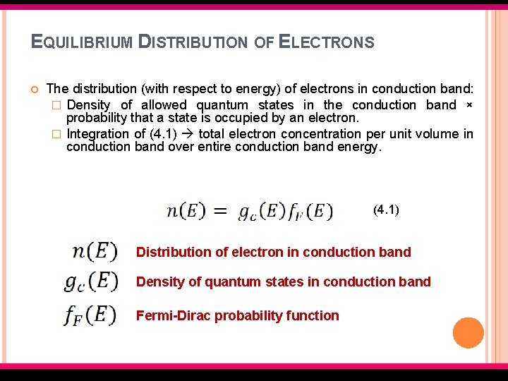
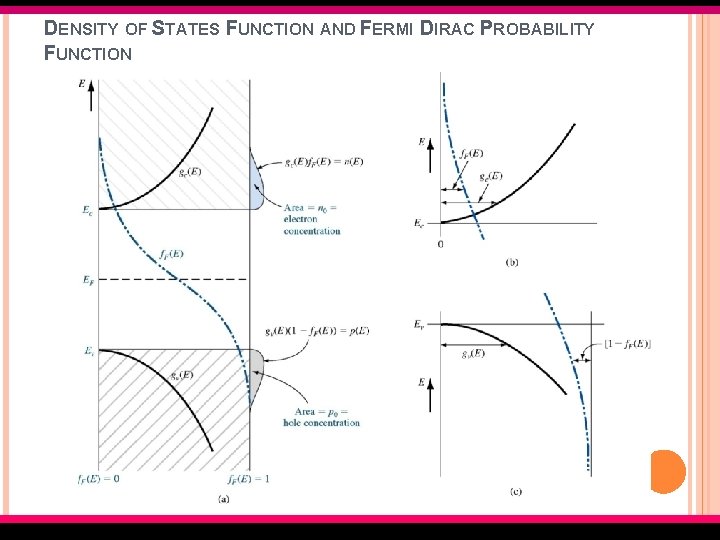
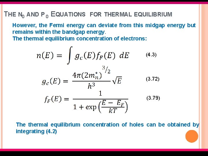
EQUILIBRIUM DISTRIBUTION OF ELECTRONS The distribution (with respect to energy) of electrons in conduction band: � Density of allowed quantum states in the conduction band × probability that a state is occupied by an electron. � Integration of (4. 1) total electron concentration per unit volume in conduction band over entire conduction band energy. (4. 1) Distribution of electron in conduction band Density of quantum states in conduction band Fermi-Dirac probability function EMT 127/3 Semiconductor Fundamentals

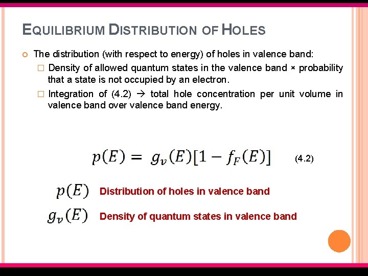
EQUILIBRIUM DISTRIBUTION OF HOLES The distribution (with respect to energy) of holes in valence band: � Density of allowed quantum states in the valence band × probability that a state is not occupied by an electron. � Integration of (4. 2) total hole concentration per unit volume in valence band over valence band energy. (4. 2) Distribution of holes in valence band Density of quantum states in valence band EMT 127/3 Semiconductor Fundamentals

THERMAL EQUILIBRIUM DISTRIBUTION OF CARRIERS In order to find thermal equilibrium electron and hole concentration to determine the position of Fermi energy, EF. Consider an ideal intrinsic semiconductor with no impurity atoms and no lattice defects in crystal. At T = 0 K, all energy states in the valence band are filled with electrons and all energy states in conduction band are empty of electrons. The Fermi energy lies somewhere between Ec and Ev. EMT 127/3 Semiconductor Fundamentals

THERMAL EQUILIBRIUM DISTRIBUTION OF CARRIERS (CONT. ) As temperature increases above 0 K, the valence electrons gain thermal energy -> few electrons in valence band may gain sufficient energy to jump to the conduction band. Electron jumped in the conduction band hole is created in valence band. In intrinsic semiconductor, electrons and holes are created in pairs by thermal energy. The no. of electrons in conduction band is equal to the no. of holes in valence band. EMT 127/3 Semiconductor Fundamentals

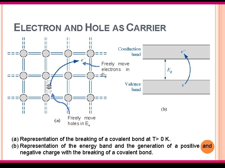
ELECTRON AND HOLE AS CARRIER Freely move electrons in Ec Freely move holes in Ev (a) Representation of the breaking of a covalent bond at T> 0 K. (b) Representation of the energy band the generation of a positive and negative charge with the breaking of a covalent bond. EMT 127/3 Semiconductor Fundamentals

DENSITY OF STATES FUNCTION AND FERMI DIRAC PROBABILITY FUNCTION EMT 127/3 Semiconductor Fundamentals

THE N 0 AND P 0 EQUATIONS FOR THERMAL EQUILIBRIUM However, the Fermi energy can deviate from this midgap energy but remains within the bandgap energy. The thermal equilibrium concentration of electrons: (4. 3) (3. 72) (3. 79) The thermal equilibrium concentration of holes can be obtained by integrating (4. 2) EMT 127/3 Semiconductor Fundamentals

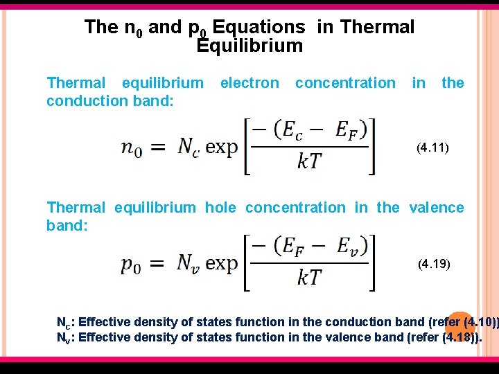
The n 0 and p 0 Equations in Thermal Equilibrium Thermal equilibrium conduction band: electron concentration in the (4. 11) Thermal equilibrium hole concentration in the valence band: (4. 19) Nc: Effective density of states function in the conduction band (refer (4. 10)) Nv: Effective density of states function in the valence band (refer (4. 18)). EMT 127/3 Semiconductor Fundamentals

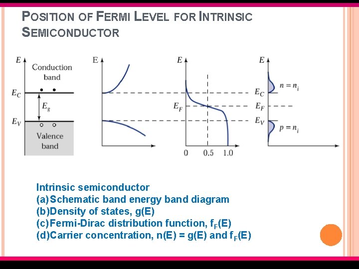
POSITION OF FERMI LEVEL FOR INTRINSIC SEMICONDUCTOR Intrinsic semiconductor (a) Schematic band energy band diagram (b) Density of states, g(E) (c) Fermi-Dirac distribution function, f. F(E) (d) Carrier concentration, n(E) = g(E) and f. F(E) EMT 127/3 Semiconductor Fundamentals

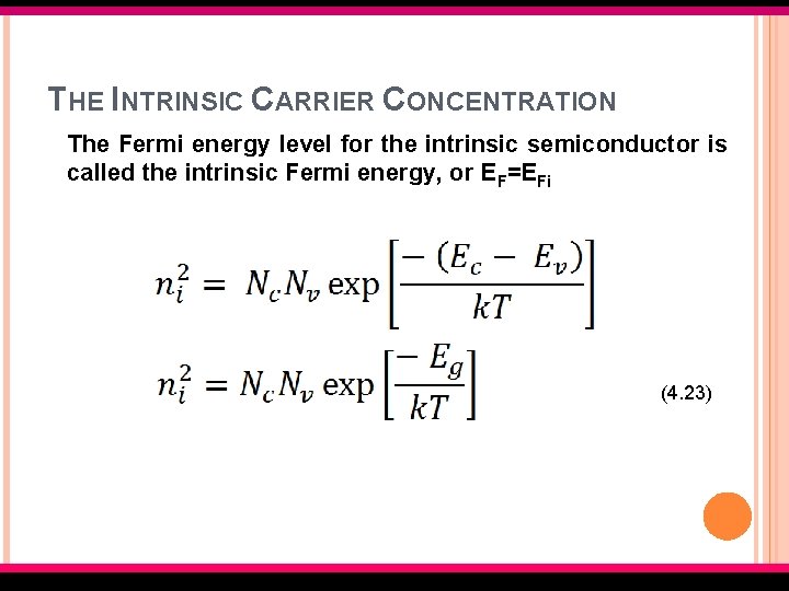
THE INTRINSIC CARRIER CONCENTRATION The Fermi energy level for the intrinsic semiconductor is called the intrinsic Fermi energy, or EF=EFi (4. 23) EMT 127/3 Semiconductor Fundamentals

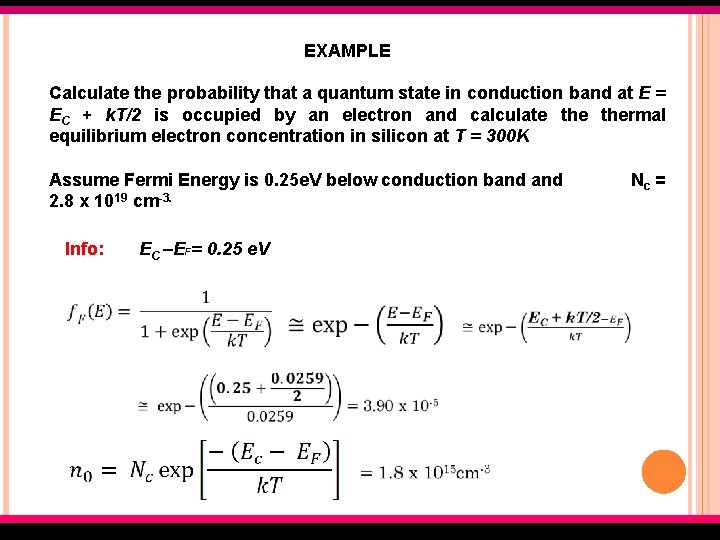
EXAMPLE Calculate the probability that a quantum state in conduction band at E = EC + k. T/2 is occupied by an electron and calculate thermal equilibrium electron concentration in silicon at T = 300 K Assume Fermi Energy is 0. 25 e. V below conduction band 2. 8 x 1019 cm-3. Info: EC –EF= 0. 25 e. V EMT 127/3 Semiconductor Fundamentals Nc =

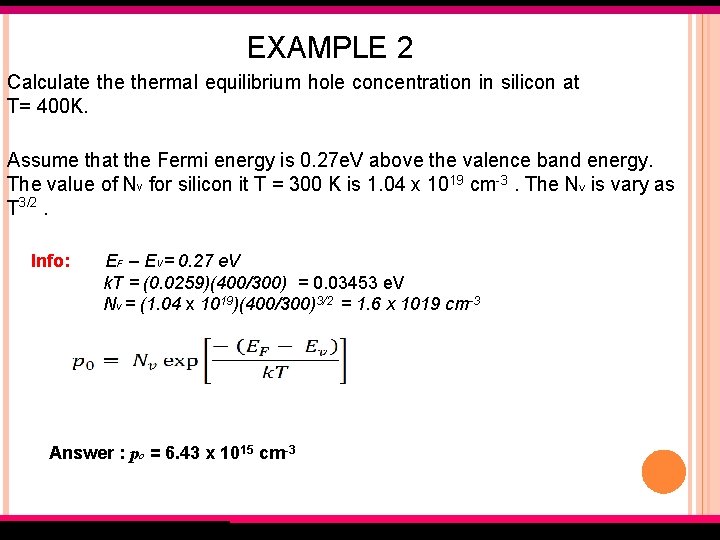
EXAMPLE 2 Calculate thermal equilibrium hole concentration in silicon at T= 400 K. Assume that the Fermi energy is 0. 27 e. V above the valence band energy. The value of Nv for silicon it T = 300 K is 1. 04 x 1019 cm-3. The NV is vary as T 3/2. Info: EF – EV= 0. 27 e. V k. T = (0. 0259)(400/300) = 0. 03453 e. V Nv = (1. 04 x 1019)(400/300)3/2 = 1. 6 x 1019 cm-3 Answer : po = 6. 43 x 1015 cm-3 EMT 127/3 Semiconductor Fundamentals

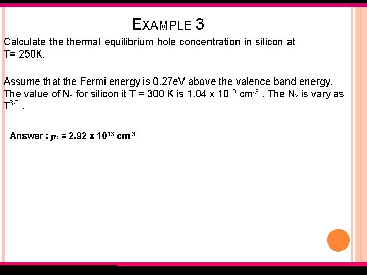
EXAMPLE 3 Calculate thermal equilibrium hole concentration in silicon at T= 250 K. Assume that the Fermi energy is 0. 27 e. V above the valence band energy. The value of Nv for silicon it T = 300 K is 1. 04 x 1019 cm-3. The NV is vary as T 3/2. Answer : po = 2. 92 x 1013 cm-3 EMT 127/3 Semiconductor Fundamentals

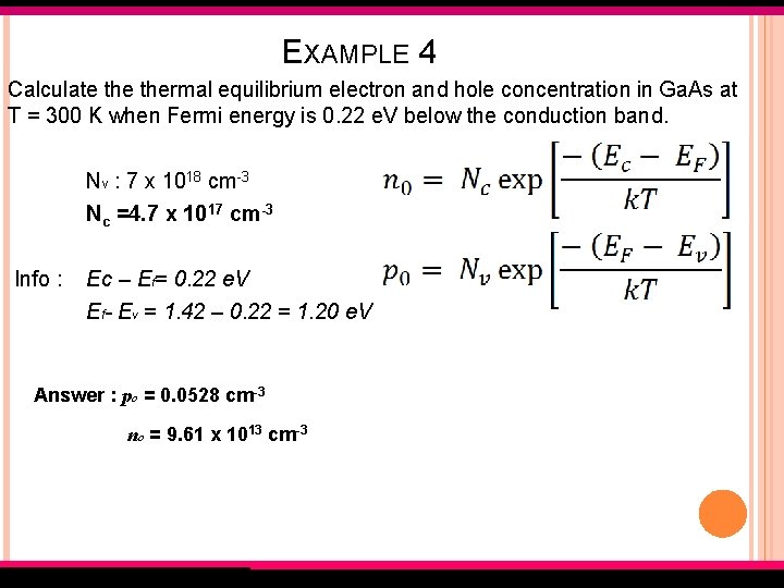
EXAMPLE 4 Calculate thermal equilibrium electron and hole concentration in Ga. As at T = 300 K when Fermi energy is 0. 22 e. V below the conduction band. Nv : 7 x 1018 cm-3 Nc =4. 7 x 1017 cm-3 Info : Ec – Ef= 0. 22 e. V Ef- E = 1. 42 – 0. 22 = 1. 20 e. V V Answer : po = 0. 0528 cm-3 no = 9. 61 x 1013 cm-3 EMT 127/3 Semiconductor Fundamentals

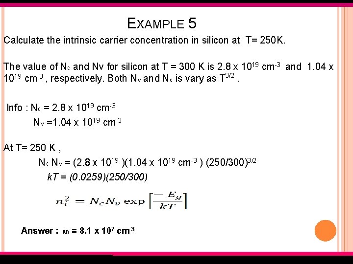
EXAMPLE 5 Calculate the intrinsic carrier concentration in silicon at T= 250 K. The value of Nc and Nv for silicon at T = 300 K is 2. 8 x 1019 cm-3 and 1. 04 x 1019 cm-3 , respectively. Both NV and NC is vary as T 3/2. Info : Nc = 2. 8 x 1019 cm-3 Nv =1. 04 x 1019 cm-3 At T= 250 K , Nc Nv = (2. 8 x 10¹⁹ )(1. 04 x 1019 cm-3 ) (250/300)3/2 k. T = (0. 0259)(250/300) Answer : ni = 8. 1 x 107 cm-3 EMT 127/3 Semiconductor Fundamentals

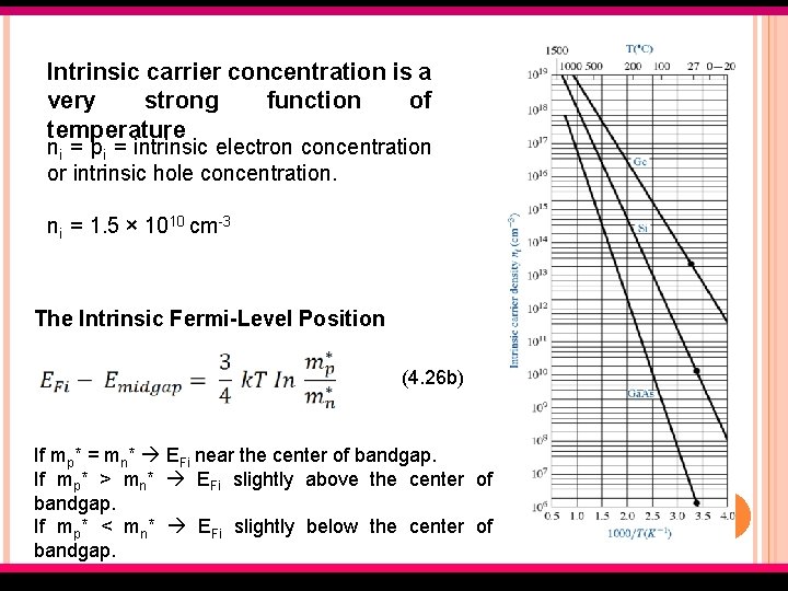
Intrinsic carrier concentration is a very strong function of temperature ni = pi = intrinsic electron concentration or intrinsic hole concentration. ni = 1. 5 × 1010 cm-3 The Intrinsic Fermi-Level Position (4. 26 b) If mp* = mn* EFi near the center of bandgap. If mp* > mn* EFi slightly above the center of bandgap. If mp* < mn* EFi slightly below the center of bandgap. EMT 127/3 Semiconductor Fundamentals

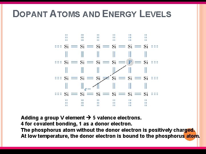
DOPANT ATOMS AND ENERGY LEVELS Adding a group V element 5 valence electrons. 4 for covalent bonding, 1 as a donor electron. The phosphorus atom without the donor electron is positively charged. At low temperature, the donor electron is bound to the phosphorus atom. EMT 127/3 Semiconductor Fundamentals

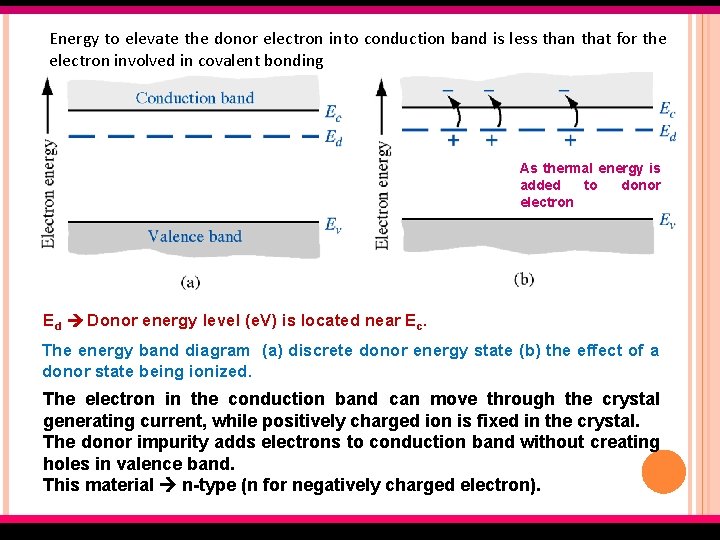
Energy to elevate the donor electron into conduction band is less than that for the electron involved in covalent bonding As thermal energy is added to donor electron Ed Donor energy level (e. V) is located near Ec. The energy band diagram (a) discrete donor energy state (b) the effect of a donor state being ionized. The electron in the conduction band can move through the crystal generating current, while positively charged ion is fixed in the crystal. The donor impurity adds electrons to conduction band without creating holes in valence band. This material n-type (n for negatively charged electron). EMT 127/3 Semiconductor Fundamentals

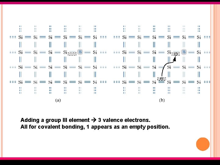
Adding a group III element 3 valence electrons. All for covalent bonding, 1 appears as an empty position. EMT 127/3 Semiconductor Fundamentals

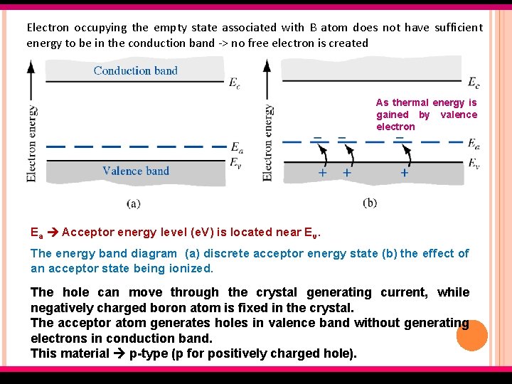
Electron occupying the empty state associated with B atom does not have sufficient energy to be in the conduction band -> no free electron is created As thermal energy is gained by valence electron Ea Acceptor energy level (e. V) is located near Ev. The energy band diagram (a) discrete acceptor energy state (b) the effect of an acceptor state being ionized. The hole can move through the crystal generating current, while negatively charged boron atom is fixed in the crystal. The acceptor atom generates holes in valence band without generating electrons in conduction band. This material p-type (p for positively charged hole). EMT 127/3 Semiconductor Fundamentals

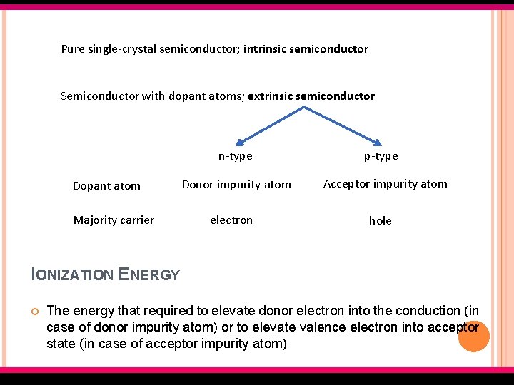
Pure single-crystal semiconductor; intrinsic semiconductor Semiconductor with dopant atoms; extrinsic semiconductor n-type Dopant atom Majority carrier Donor impurity atom electron p-type Acceptor impurity atom hole IONIZATION ENERGY The energy that required to elevate donor electron into the conduction (in case of donor impurity atom) or to elevate valence electron into acceptor state (in case of acceptor impurity atom) EMT 127/3 Semiconductor Fundamentals

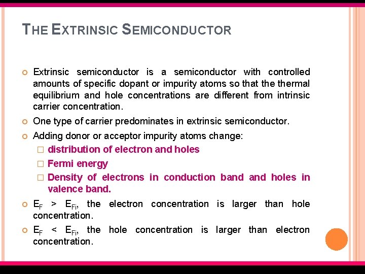
THE EXTRINSIC SEMICONDUCTOR Extrinsic semiconductor is a semiconductor with controlled amounts of specific dopant or impurity atoms so that thermal equilibrium and hole concentrations are different from intrinsic carrier concentration. One type of carrier predominates in extrinsic semiconductor. Adding donor or acceptor impurity atoms change: � distribution of electron and holes � Fermi energy � Density of electrons in conduction band holes in valence band. EF > EFi, the electron concentration is larger than hole concentration. EF < EFi, the hole concentration is larger than electron concentration. EMT 127/3 Semiconductor Fundamentals

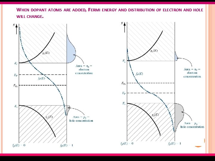
WHEN DOPANT ATOMS ARE ADDED, FERMI ENERGY AND DISTRIBUTION OF ELECTRON AND HOLE WILL CHANGE. EMT 127/3 Semiconductor Fundamentals

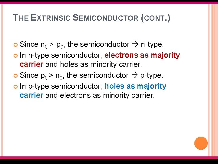
THE EXTRINSIC SEMICONDUCTOR (CONT. ) Since n 0 > p 0, the semiconductor n-type. In n-type semiconductor, electrons as majority carrier and holes as minority carrier. Since p 0 > n 0, the semiconductor p-type. In p-type semiconductor, holes as majority carrier and electrons as minority carrier. EMT 127/3 Semiconductor Fundamentals

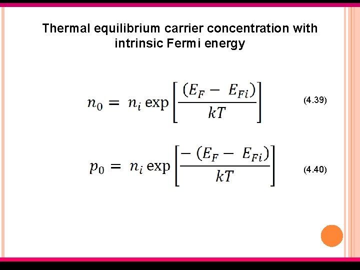
Thermal equilibrium carrier concentration with intrinsic Fermi energy (4. 39) (4. 40) EMT 127/3 Semiconductor Fundamentals

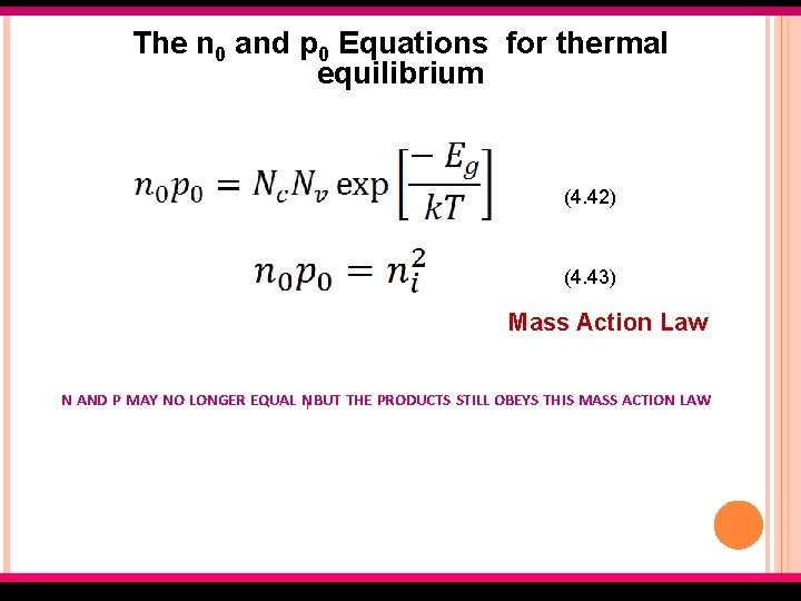
The n 0 and p 0 Equations for thermal equilibrium (4. 42) (4. 43) Mass Action Law N AND P MAY NO LONGER EQUAL NI BUT THE PRODUCTS STILL OBEYS THIS MASS ACTION LAW EMT 127/3 Semiconductor Fundamentals

DEGENERATE &NONDEGENERATE SEMICONDUCTORS When dopant is added, we assumed that the concentration of dopant atoms added is small compared to density of host/semiconductor atoms. The small no. of impurity are spread far enough that no interaction between donor electrons e. g. n-type material. It is assumed impurities introduce discrete and noninteracting donor energy states in n-type semiconductor and discrete and noninteracting acceptor state in p-type semicondictor. Referred to as nondegenerate semiconductor. EMT 127/3 Semiconductor Fundamentals

DEGENERATE &NONDEGENERATE SEMICONDUCTORS If the impurity concentration increases, the distances between impurity atoms decreases and a point be reached when donor electrons interact with each other. So the single discrete donor energy will split into band of energies. And if the donor concentration further increases, the band of donor states widen and may overlap the bottom of conduction band. It occurs when donor concentration becomes comparable with effective density of states. The concentration of electrons in conduction band exceeds the density states Nc, the Fermi energy lies within conduction band. Referred to as degenerate semiconductor. EMT 127/3 Semiconductor Fundamentals

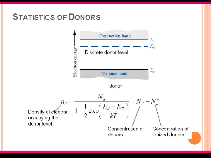
STATISTICS OF DONORS EMT 127/3 Semiconductor Fundamentals

STATISTICS OF ACCEPTORS EMT 127/3 Semiconductor Fundamentals

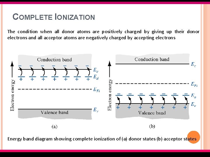
COMPLETE IONIZATION The condition when all donor atoms are positively charged by giving up their donor electrons and all acceptor atoms are negatively charged by accepting electrons Energy band diagram showing complete ionization of (a) donor states (b) acceptor states EMT 127/3 Semiconductor Fundamentals

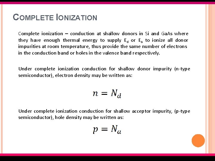
COMPLETE IONIZATION Complete ionization – conduction at shallow donors in Si and Ga. As where they have enough thermal energy to supply Ed or Ea to ionize all donor impurities at room temperature, thus provide the same number of electrons in the conduction band or holes in the valence band respectively. Under complete ionization conduction for shallow donor impurity (n-type semiconductor), electron density may be written as: Under complete ionization conduction for shallow acceptor impurity, (p-type semiconductor), hole density may be written as: EMT 127/3 Semiconductor Fundamentals

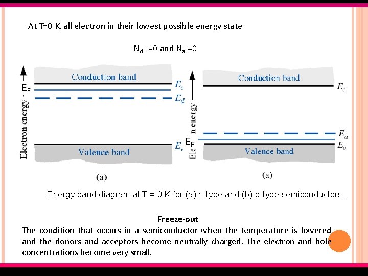
At T=0 K, all electron in their lowest possible energy state Nd +=0 and Na-=0 Energy band diagram at T = 0 K for (a) n-type and (b) p-type semiconductors. Freeze-out The condition that occurs in a semiconductor when the temperature is lowered and the donors and acceptors become neutrally charged. The electron and hole concentrations become very small. EMT 127/3 Semiconductor Fundamentals

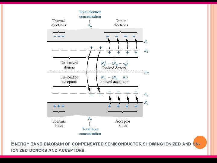
CHARGE NEUTRALITY In thermal equilibrium, the semiconductor crystal is electrically neutral. Net charge density is zero. A compensated semiconductor contains both donor and acceptor impurity atoms in the same region. Example: diffusing acceptor impurities into n-type material or diffusing donor impurities into p-type material. N-type compensated semiconductor occurs when Nd > N a. If Nd = Na complete compensated semiconductor. EMT 127/3 Semiconductor Fundamentals

ENERGY BAND DIAGRAM OF COMPENSATED SEMICONDUCTOR SHOWING IONIZED AND UNIONIZED DONORS AND ACCEPTORS. EMT 127/3 Semiconductor Fundamentals

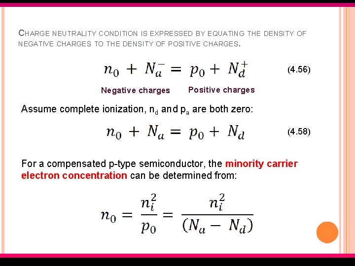
CHARGE NEUTRALITY CONDITION IS EXPRESSED BY EQUATING THE DENSITY OF NEGATIVE CHARGES TO THE DENSITY OF POSITIVE CHARGES. (4. 56) Negative charges Positive charges Assume complete ionization, nd and pa are both zero: (4. 58) For a compensated p-type semiconductor, the minority carrier electron concentration can be determined from: EMT 127/3 Semiconductor Fundamentals

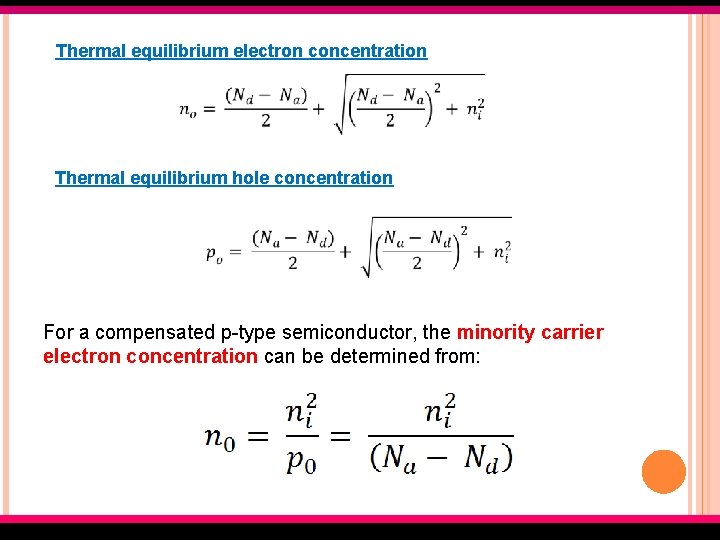
Thermal equilibrium electron concentration Thermal equilibrium hole concentration For a compensated p-type semiconductor, the minority carrier electron concentration can be determined from: EMT 127/3 Semiconductor Fundamentals

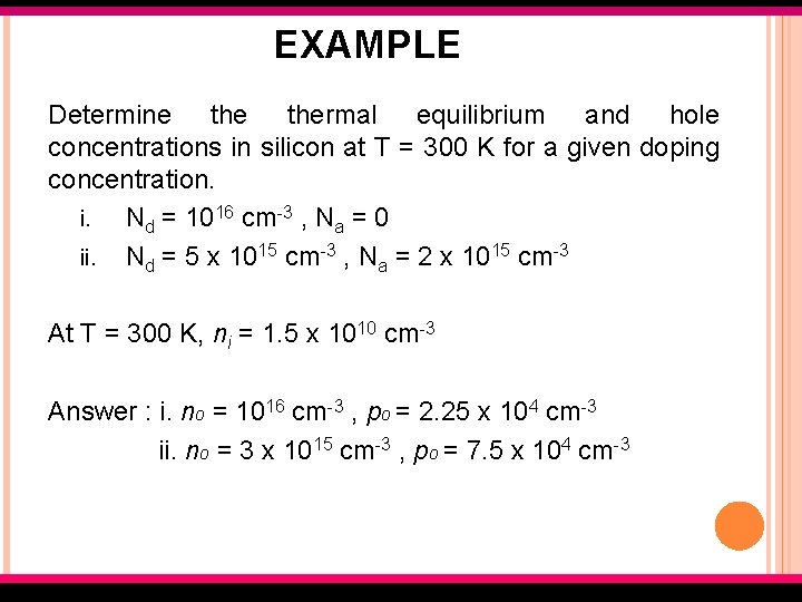
EXAMPLE Determine thermal equilibrium and hole concentrations in silicon at T = 300 K for a given doping concentration. i. Nd = 1016 cm-3 , Na = 0 ii. Nd = 5 x 1015 cm-3 , Na = 2 x 1015 cm-3 At T = 300 K, ni = 1. 5 x 1010 cm-3 Answer : i. no = 1016 cm-3 , po = 2. 25 x 104 cm-3 ii. no = 3 x 1015 cm-3 , po = 7. 5 x 104 cm-3 EMT 127/3 Semiconductor Fundamentals

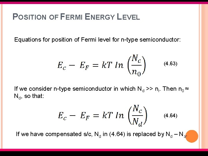
POSITION OF FERMI ENERGY LEVEL Equations for position of Fermi level for n-type semiconductor: (4. 63) If we consider n-type semiconductor in which Nd >> ni. Then n 0 ≈ Nd, so that: (4. 64) If we have compensated s/c, Nd in (4. 64) is replaced by Nd – Na. EMT 127/3 Semiconductor Fundamentals

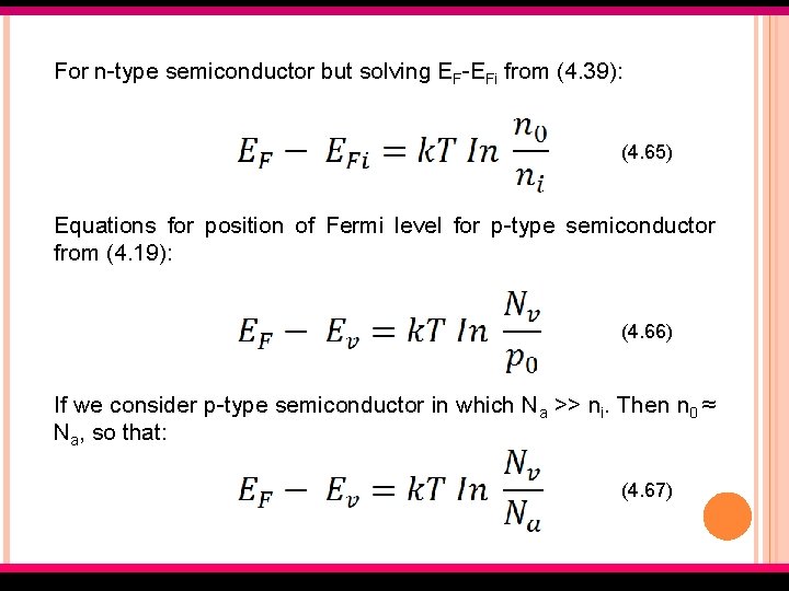
For n-type semiconductor but solving EF-EFi from (4. 39): (4. 65) Equations for position of Fermi level for p-type semiconductor from (4. 19): (4. 66) If we consider p-type semiconductor in which Na >> ni. Then n 0 ≈ Na, so that: (4. 67) EMT 127/3 Semiconductor Fundamentals

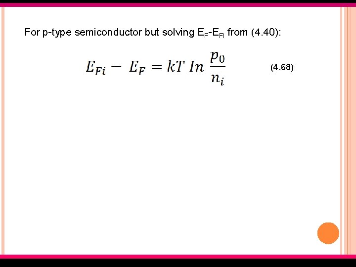
For p-type semiconductor but solving EF-EFi from (4. 40): (4. 68) EMT 127/3 Semiconductor Fundamentals

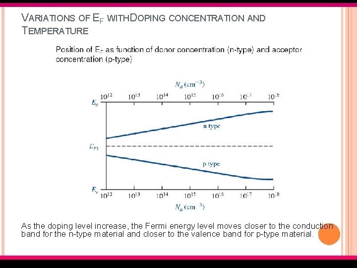
VARIATIONS OF EF WITH DOPING CONCENTRATION AND TEMPERATURE As the doping level increase, the Fermi energy level moves closer to the conduction band for the n-type material and closer to the valence band for p-type material. EMT 127/3 Semiconductor Fundamentals

CHECK AND BALANCE Ability to describe and differentiate the following idea: � Energy band diagram � Density of states � Carrier distribution � Acceptor and donor energy level � electron and holes terminology � Fermi level position for extrinsic and intrinsic semiconductor. EMT 127/3 Semiconductor Fundamentals