Lesson 3 Intrinsic and Extrinsic Semiconductor 1 Jyoti
 Jyoti Patel")


 N-Type SC/Donar • Impurity is pentavalent. 1. Crystalline structure at 0 k")


 P-Type SC/Acceptor/+ve Type SC • Impurity is trivalent. 1. Crystalline structure at 0")


 negatively charged b) Positively")

- Slides: 23
Lesson 3 Intrinsic and Extrinsic Semiconductor (1) Jyoti Patel
ØElectrical Properties of Ge and Si Properties Atomic No. Density of atoms Intrinsic concentration at 300 k Intrinsic Resistivity at 300 k Leakage current Maximum operating temperature Ge Si 32 4. 421 x 1022 2. 5 x 10¹³ 14 5 x 10²² 1. 5 x 10¹⁰ 45 2, 30, 000 µA 75˚C n. A 175˚C
ØWhy Si is preferred than Ge? • • • Smaller Leakage current. High power handling capacity. High temperature applications. Plenty available on the surface of earth. Cheaper or economical. Favorable property to form Si. O 2 Ø Disadvantage of Si : • Si when exposed at 1400˚C temperature, it melts and when reacted with O 2 gives Si. O 2 Si (1400˚C ) + O 2 = Si. O 2
Que : IC fabrication in Si. O 2 is for providing what? Ans : For providing Insulation Ø Intrinsic Semiconductor • Also called as non-degenerate semiconductor. 1. Crystalline structure at 0 k
• Sharing of electrons with neighboring atoms is called Covalent Bonding. • In 1 Covalent bond there will be 2 valence electrons. • At 0 k all valence electrons are in perfect covalent bonding. So at 0 k will be working as an Insulator. 2. Crystalline structure at 300 k
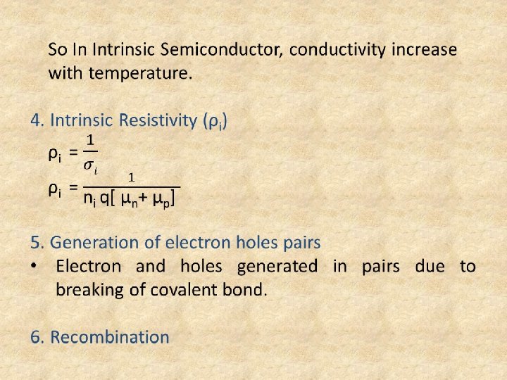
• When covalent bond is broken it will create 1 electron and 1 hole. • Hole is defined as deficiency of an electron in the broken covalent bond. • In Intrinsic Semiconductor (n = p = ni) 3. Intrinsic Conductivity σi = nq. µn + pq. µp , but(n = p = ni) σi = ni q[µn + µp] σi α ni ni α T 3/2 • Hence, ni increases with temperature as a non linear variation.
• Free electron and hole both will disappear and covalent bond is created. 7. Carrier life time (τ) • Interval of time from breaking of its covalent bond untill it’s recombination. • Range is from microseconds to milliseconds. 8. Disadvantage of Intrinsic Semiconductor • Conductivity is very small Note: The only Semiconductor device fabricated with Intrinsic Semiconductor is Pin Diode
Ø Doping • Adding impurities to the semiconductor is doping. • Increase carrier concentration. • Standard doping levels - Moderate doping = 1 : [106 to 108] - Lightly doping = 1 : 1011 - Highly (Heavily) doping = 1 : 103 • Minimum doping required to convert intrinsic into extrinsic semiconductor is 1 : 108 • Que : Moderate doping refers to? Ans : a) 1 : 106 b) 1 : 105 c) 1 : 103 d) 1 : 108
• Impurity types - Trivalent/acceptor Impurities : B - Pentavalent/donor Impurities : P Al As Ga Sb In Bi • Que : Conductivity Increase by how much with 1 : 108 doping in Ge ? Ans : Increases by 12 times Ø Extrinsic Semiconductor • Also called as degenerate semiconductor/Doped Semiconductor Two types : N type SC/Donar P type SC/Acceptors
a) N-Type SC/Donar • Impurity is pentavalent. 1. Crystalline structure at 0 k
• Donar Energy level is a discrete energy level created just below the C. B • Free electron is having a force of attraction to parent atom. • At 0 k the 5 th electron will be existing in the donar energy level. • 5 th electron is not in covalent bonding and even its not free electron but it is a bonded electron to a parent atom. • At 0 k the 5 th electron of all impurity atoms exist in the donar energy level. • Que : How much additional energy is required to detach the bonded electron? Ans : 0. 01 for Ge and 0. 05 for Si
2. Crystalline structure at 300 k
• Donar energy level Ionisation : Refers to the 5 th electron moving from donar energy level to the conduction band. • Donar level Ionisation increase with increase in temperature. • At 300 k the 5 th electron of all the impurity atoms has shifted from donar energy level into C. B and donar energy level will become empty energy level. • Above 300 k there is no donar level Ionisation. • Que : Why it’s n>>p in N type semiconductor? Ans : The conc. of free electrons in C. B is far greater than the conc. of holes in V. B. So, electrons are the majority carriers and holes are minority.
• Majority carriers will contribute more current with less noise. • Minority carriers will contribute less current with less noise. • Minority carrier noise is thermal noise and it increase with the temperature. • Conductivity due to minority carriers is almost negligible. So, Majority > 99. 99 % Minority < 0. 01 % • The condition for n type semiconductor is : n > ni p < ni
3. Law of electrical Neutrality ND + P = N A + N Where, ND = density of donar atoms NA = density of acceptor atoms So, here NA = 0 ND + p = n Or n ≈ ND 4. Conductivity of N – type semiconductor σN = nq. µn + pq. µp σN ≈ ND q. µn
b) P-Type SC/Acceptor/+ve Type SC • Impurity is trivalent. 1. Crystalline structure at 0 k
• Acceptor Energy level is discrete energy level created just above the V. B • Acceptor Energy level is energy level of trivalent atoms added to the semiconductor. • P Type SC at 0 k will be working as an insulator. • Every impurity atom will be receiving one electron to complete its covalent bonding so P type is also called as acceptor. 2. Crystalline structure at 300 k • At 300 k because of thermal energy large no. of covalent bonds will be broken and equal no. of electrons and holes are created.
• These electrons will be moving from V. B into Energy level to complete the bonding and very few electrons will be moving from V. B to C. B
• Hole concentration in V. B is greater than electron concentration in C. B • Conductivity due to minority carriers is almost negligible. So, Majority > 99. 99 % Minority < 0. 01 % • The condition for p type semiconductor is : P > ni n < ni • Therefore, Holes -> Majority carriers Electrons -> Minority carriers
3. Law of electrical Neutrality ND + P = N A + N Where, ND = density of donar atoms NA = density of acceptor atoms So, here ND = 0 NA + n = p Or p ≈ NA 4. Conductivity of P-Type semiconductor σP = nq. µn + pq. µp σP ≈ NA q. µp
• Que : N-Type Semiconductor is? Ans : a) negatively charged b) Positively charged c) No charge at all d) Electrically neutral • Que : N-Type Semiconductor is? Ans : Electrically neutral
Thanks For Watching