A promising approach for monolithic integration of IIIV

- Slides: 1

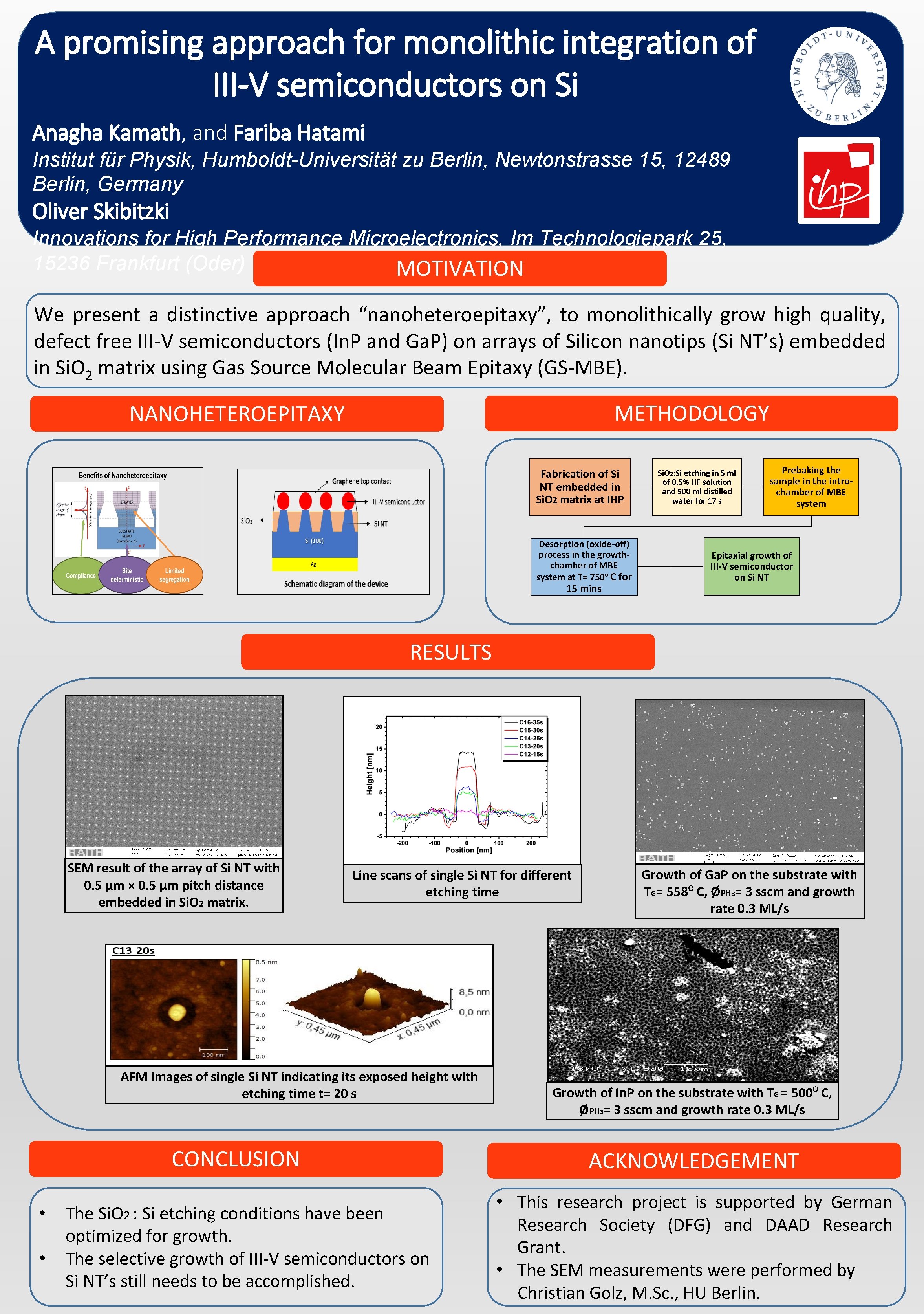
A promising approach for monolithic integration of III-V semiconductors on Si Anagha Kamath, and Fariba Hatami Institut für Physik, Humboldt-Universität zu Berlin, Newtonstrasse 15, 12489 Berlin, Germany Oliver Skibitzki Innovations for High Performance Microelectronics, Im Technologiepark 25, 15236 Frankfurt (Oder) MOTIVATION We present a distinctive approach “nanoheteroepitaxy”, to monolithically grow high quality, defect free III-V semiconductors (In. P and Ga. P) on arrays of Silicon nanotips (Si NT’s) embedded in Si. O 2 matrix using Gas Source Molecular Beam Epitaxy (GS-MBE). METHODOLOGY NANOHETEROEPITAXY Fabrication of Si NT embedded in Si. O 2 matrix at IHP Desorption (oxide-off) process in the growthchamber of MBE system at T= 750 o C for 15 mins Si. O 2: Si etching in 5 ml of 0. 5% HF solution and 500 ml distilled water for 17 s Prebaking the sample in the introchamber of MBE system Epitaxial growth of III-V semiconductor on Si NT RESULTS SEM result of the array of Si NT with 0. 5 µm × 0. 5 µm pitch distance embedded in Si. O 2 matrix. Line scans of single Si NT for different etching time AFM images of single Si NT indicating its exposed height with etching time t= 20 s CONCLUSION • • The Si. O 2 : Si etching conditions have been optimized for growth. The selective growth of III-V semiconductors on Si NT’s still needs to be accomplished. Growth of Ga. P on the substrate with o TG= 558 C, ØPH 3= 3 sscm and growth rate 0. 3 ML/s o Growth of In. P on the substrate with TG = 500 C, ØPH 3= 3 sscm and growth rate 0. 3 ML/s ACKNOWLEDGEMENT • This research project is supported by German Research Society (DFG) and DAAD Research Grant. • The SEM measurements were performed by Christian Golz, M. Sc. , HU Berlin.