Semiconductor detectors An introduction to semiconductor detector physics
- Slides: 30

Semiconductor detectors An introduction to semiconductor detector physics as applied to particle physics

Contents 4 lectures – can’t cover much of a huge field • • Introduction Fundamentals of operation The micro-strip detector Radiation hardness issues

Lecture 2 – lots of details • • Simple diode theory Fabrication Energy deposition Signal formation

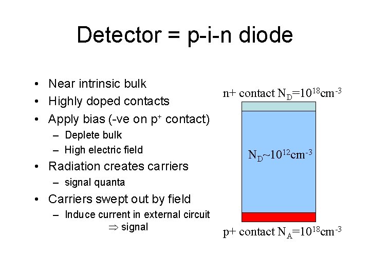
Detector = p-i-n diode • Near intrinsic bulk • Highly doped contacts • Apply bias (-ve on p+ contact) – Deplete bulk – High electric field • Radiation creates carriers n+ contact ND=1018 cm-3 ND~1012 cm-3 – signal quanta • Carriers swept out by field – Induce current in external circuit signal p+ contact NA=1018 cm-3

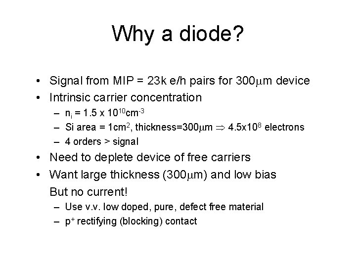
Why a diode? • Signal from MIP = 23 k e/h pairs for 300 m device • Intrinsic carrier concentration – ni = 1. 5 x 1010 cm-3 – Si area = 1 cm 2, thickness=300 m 4. 5 x 10⁸ electrons – 4 orders > signal • Need to deplete device of free carriers • Want large thickness (300 m) and low bias But no current! – Use v. v. low doped, pure, defect free material – p+ rectifying (blocking) contact

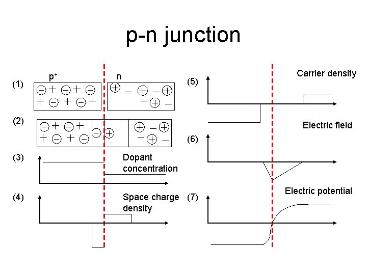
p-n junction (1) p+ n (5) (2) Carrier density Electric field (6) (3) Dopant concentration (4) Space charge (7) density Electric potential

p-n junction 1) Take your samples – these are neutral but doped samples: p+ and n 2) Bring together – free carriers move o two forces drift and diffusion o In stable state Jdiffusion (concentration density) = Jdrift (e-field) 3) p+ area has higher doping concentration (in this case) than the n region 4) Fixed charge region with no free carriers

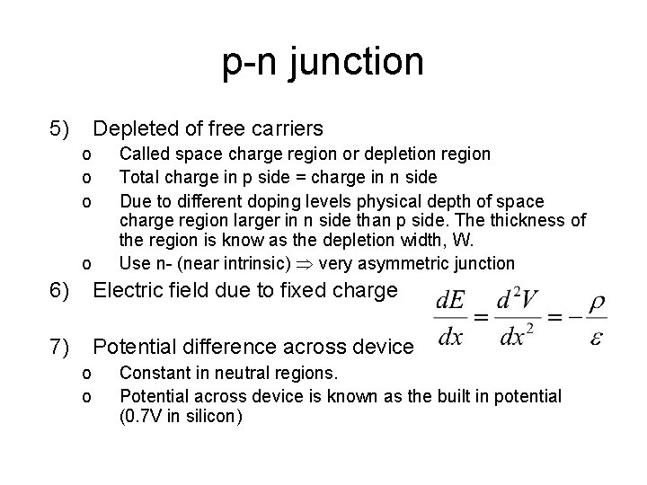
p-n junction 5) Depleted of free carriers o o Called space charge region or depletion region Total charge in p side = charge in n side Due to different doping levels physical depth of space charge region larger in n side than p side. The thickness of the region is know as the depletion width, W. Use n- (near intrinsic) very asymmetric junction 6) Electric field due to fixed charge 7) Potential difference across device o o Constant in neutral regions. Potential across device is known as the built in potential (0. 7 V in silicon)

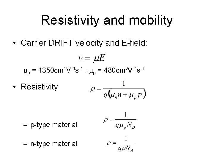
Resistivity and mobility • Carrier DRIFT velocity and E-field: n = 1350 cm 2 V-1 s-1 : p = 480 cm 2 V-1 s-1 • Resistivity – p-type material – n-type material

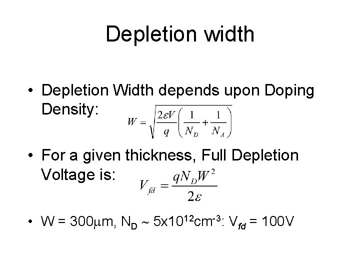
Depletion width • Depletion Width depends upon Doping Density: • For a given thickness, Full Depletion Voltage is: • W = 300 m, ND 5 x 1012 cm-3: Vfd = 100 V

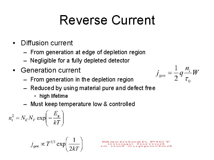
Reverse Current • Diffusion current – From generation at edge of depletion region – Negligible for a fully depleted detector • Generation current – From generation in the depletion region – Reduced by using material pure and defect free • high lifetime – Must keep temperature low & controlled

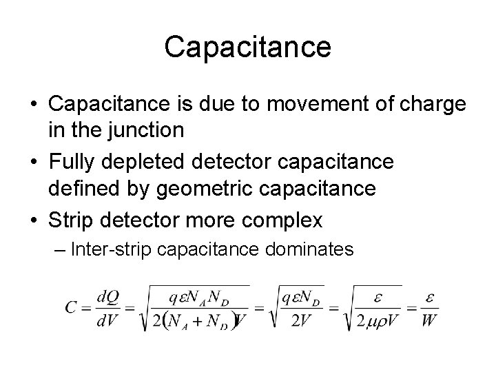
Capacitance • Capacitance is due to movement of charge in the junction • Fully depleted detector capacitance defined by geometric capacitance • Strip detector more complex – Inter-strip capacitance dominates

Noise • Depends upon detector capacitance and reverse current • Depends upon electronics design • Function of signal shaping time • Lower capacitance lower noise • Faster electronics noise contribution from reverse current less significant

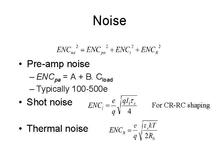
Noise • Pre-amp noise – ENCpa = A + B. Cload – Typically 100 -500 e • Shot noise • Thermal noise For CR-RC shaping

Fabrication • Use very pure material – High resistivity • Low bias to deplete device – Easy of operation, away from breakdown, charge spreading for better position resolution – Low defect concentration • No extra current sources • No trapping of charge carriers • Planar fabrication techniques – Make p-i-n diode – pattern of implants define type of detector (pixel/strip) – extra guard rings used to control surface leakage currents – metallisation structure effects E-field mag limits max bias

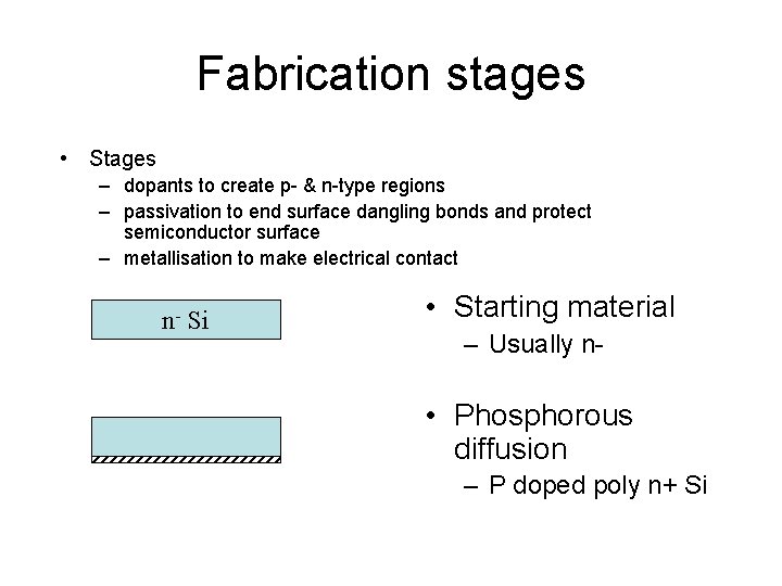
Fabrication stages • Stages – dopants to create p- & n-type regions – passivation to end surface dangling bonds and protect semiconductor surface – metallisation to make electrical contact n- Si • Starting material – Usually n- • Phosphorous diffusion – P doped poly n+ Si

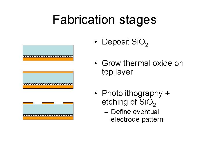
Fabrication stages • Deposit Si. O 2 • Grow thermal oxide on top layer • Photolithography + etching of Si. O 2 – Define eventual electrode pattern

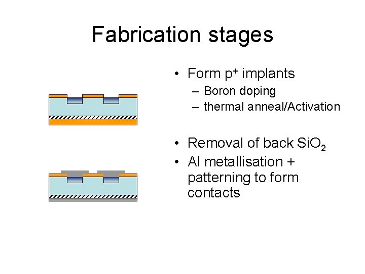
Fabrication stages • Form p+ implants – Boron doping – thermal anneal/Activation • Removal of back Si. O 2 • Al metallisation + patterning to form contacts

Fabrication • Tricks for low leakage currents – low temperature processing • simple, cheap • marginal activation of implants, can’t use IC tech – gettering • very effective at removal of contaminants • complex

Energy Deposition • Charge particles – Bethe-Bloch – Bragg Peak • Not covered – Neutrons – Gamma Rays • Rayleigh scattering, Photo-electric effect, Compton scattering, Pair production

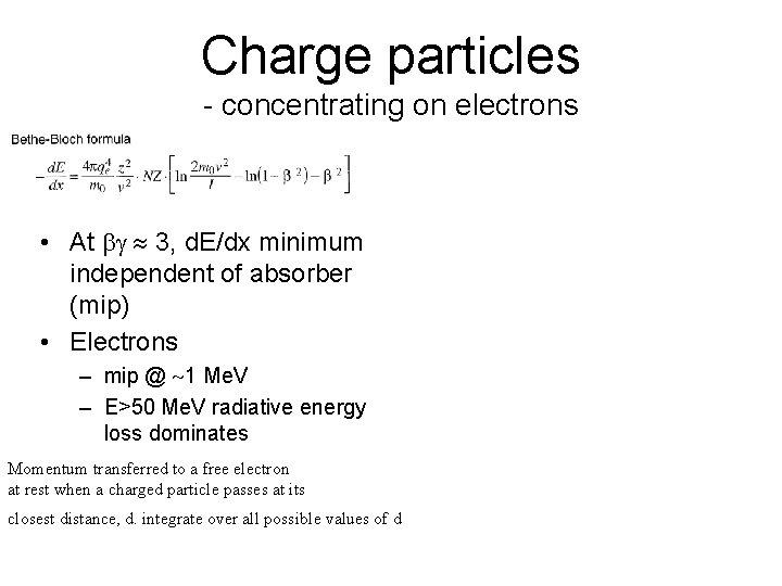
Charge particles - concentrating on electrons • At 3, d. E/dx minimum independent of absorber (mip) • Electrons – mip @ 1 Me. V – E>50 Me. V radiative energy loss dominates Momentum transferred to a free electron at rest when a charged particle passes at its closest distance, d. integrate over all possible values of d

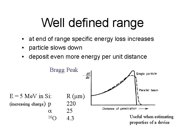
Well defined range • at end of range specific energy loss increases • particle slows down • deposit even more energy per unit distance Bragg Peak E = 5 Me. V in Si: (increasing charge) p 16 O R ( m) 220 25 4. 3 Useful when estimating properties of a device

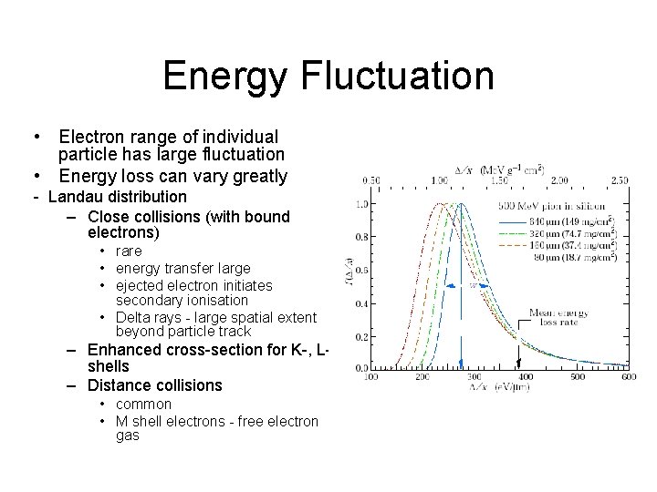
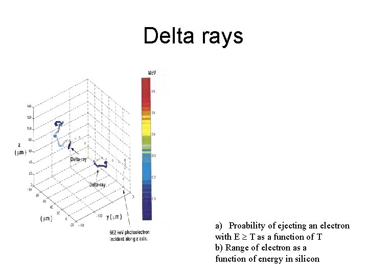
Energy Fluctuation • Electron range of individual particle has large fluctuation • Energy loss can vary greatly - Landau distribution – Close collisions (with bound electrons) • rare • energy transfer large • ejected electron initiates secondary ionisation • Delta rays - large spatial extent beyond particle track – Enhanced cross-section for K-, Lshells – Distance collisions • common • M shell electrons - free electron gas

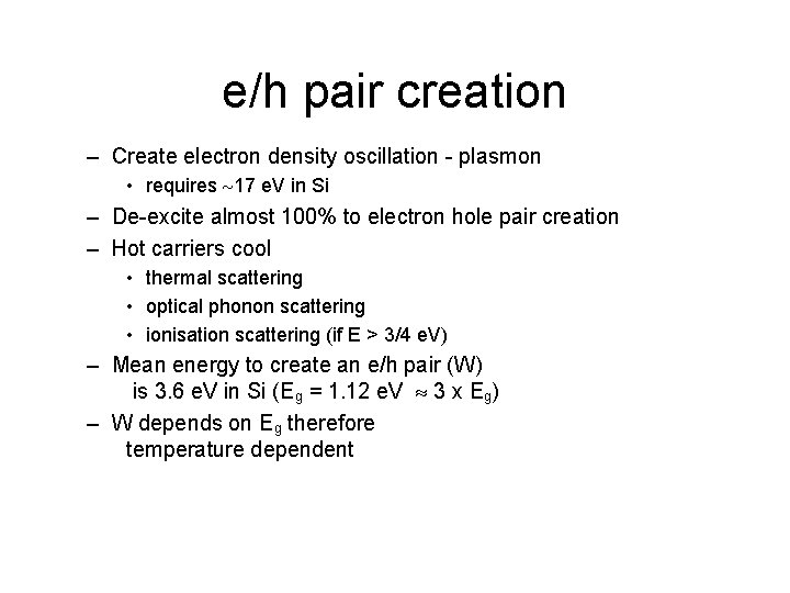
e/h pair creation – Create electron density oscillation - plasmon • requires 17 e. V in Si – De-excite almost 100% to electron hole pair creation – Hot carriers cool • thermal scattering • optical phonon scattering • ionisation scattering (if E > 3/4 e. V) – Mean energy to create an e/h pair (W) is 3. 6 e. V in Si (Eg = 1. 12 e. V 3 x Eg) – W depends on Eg therefore temperature dependent

Delta rays a) Proability of ejecting an electron with E T as a function of T b) Range of electron as a function of energy in silicon

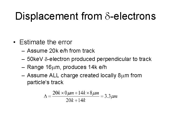
Displacement from -electrons • Estimate the error – – Assume 20 k e/h from track 50 ke. V -electron produced perpendicular to track Range 16 m, produces 14 k e/h Assume ALL charge created locally 8 m from particle’s track

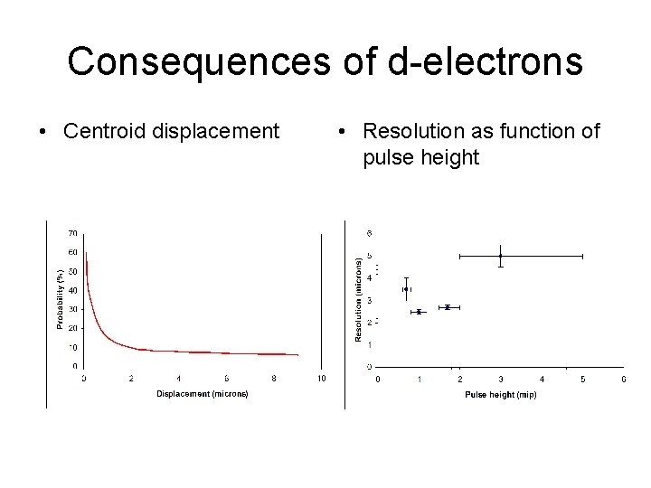
Consequences of d-electrons • Centroid displacement • Resolution as function of pulse height

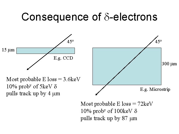
Consequence of -electrons 45º 15 m E. g. CCD Most probable E loss = 3. 6 ke. V 10% proby of 5 ke. V pulls track up by 4 m 300 m E. g. Microstrip Most probable E loss = 72 ke. V 10% proby of 100 ke. V pulls track up by 87 m

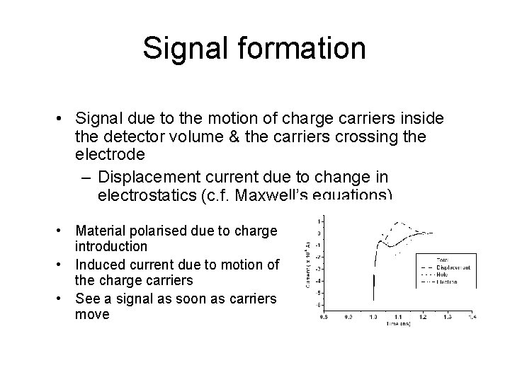
Signal formation • Signal due to the motion of charge carriers inside the detector volume & the carriers crossing the electrode – Displacement current due to change in electrostatics (c. f. Maxwell’s equations) • Material polarised due to charge introduction • Induced current due to motion of the charge carriers • See a signal as soon as carriers move

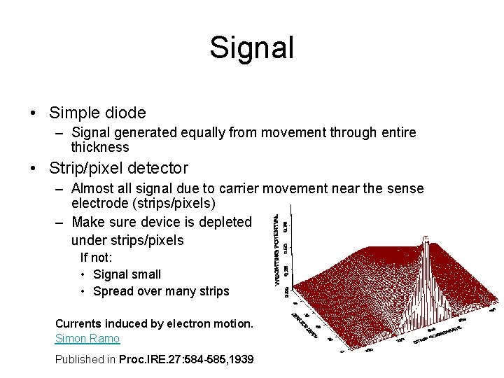
Signal • Simple diode – Signal generated equally from movement through entire thickness • Strip/pixel detector – Almost all signal due to carrier movement near the sense electrode (strips/pixels) – Make sure device is depleted under strips/pixels If not: • Signal small • Spread over many strips Currents induced by electron motion. Simon Ramo Published in Proc. IRE. 27: 584 -585, 1939