Chapter 1 Fundamental SolidState Principles Semiconductor n Semiconductor

- Slides: 22

Chapter 1 Fundamental Solid-State Principles

Semiconductor n Semiconductor - An element that is neither an insulator nor a conductor.

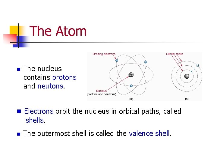
The Atom n The nucleus contains protons and neutons. n Electrons orbit the nucleus in orbital paths, called shells. n The outermost shell is called the valence shell.

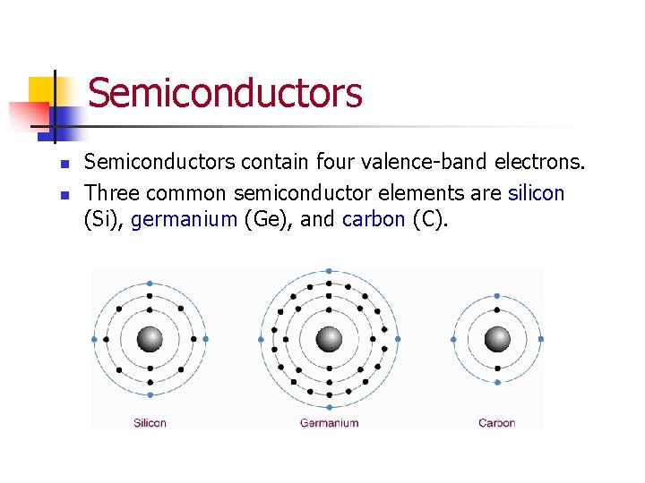
Semiconductors n n Semiconductors contain four valence-band electrons. Three common semiconductor elements are silicon (Si), germanium (Ge), and carbon (C).

Electrons and Orbital Shells n n Energy gap – The difference between the energy levels of any two orbital shells. Band – Another name for an orbital shell. Electron-volt (e. V) – The energy absorbed by an electron when it is subjected to a 1 V difference of potential. Conduction band – The band outside the valence shell.

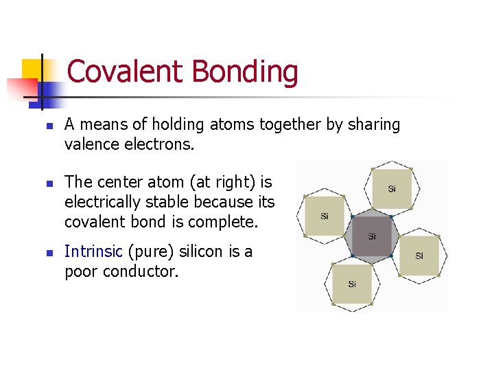
Covalent Bonding n n n A means of holding atoms together by sharing valence electrons. The center atom (at right) is electrically stable because its covalent bond is complete. Intrinsic (pure) silicon is a poor conductor.

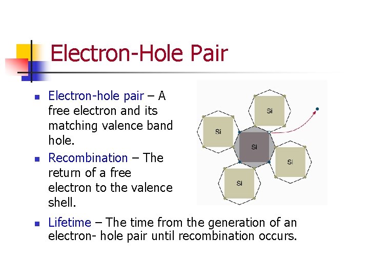
Electron-Hole Pair n n n Electron-hole pair – A free electron and its matching valence band hole. Recombination – The return of a free electron to the valence shell. Lifetime – The time from the generation of an electron- hole pair until recombination occurs.

Doping The process of adding impurity elements to intrinsic semiconductors. n n Trivalent element – One that has three valence electrons. p-type material – A semiconductor that has added trivalent impurities. Pentavalent element – One that has five valence electrons. n-type material – A semiconductor that has added pentavalent impurities.

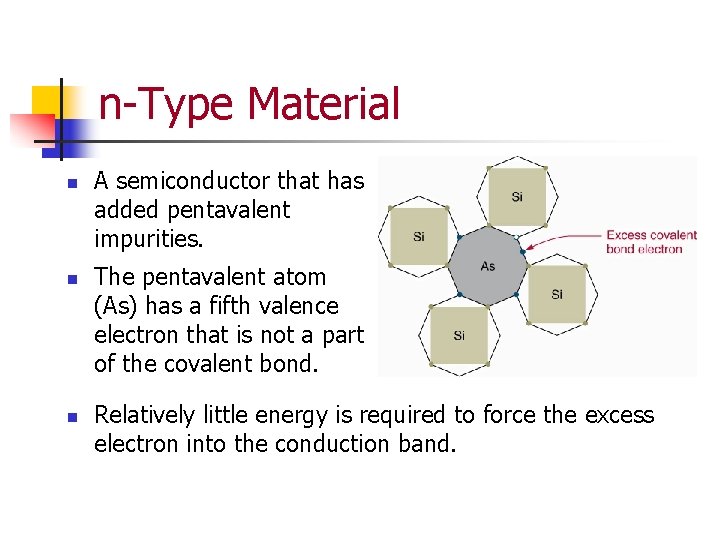
n-Type Material n n n A semiconductor that has added pentavalent impurities. The pentavalent atom (As) has a fifth valence electron that is not a part of the covalent bond. Relatively little energy is required to force the excess electron into the conduction band.

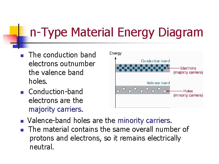
n-Type Material Energy Diagram n n The conduction band electrons outnumber the valence band holes. Conduction-band electrons are the majority carriers. Valence-band holes are the minority carriers. The material contains the same overall number of protons and electrons, so it remains electrically neutral.

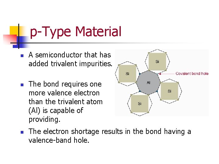
p-Type Material n n n A semiconductor that has added trivalent impurities. The bond requires one more valence electron than the trivalent atom (Al) is capable of providing. The electron shortage results in the bond having a valence-band hole.

p-Type Material Energy Diagram n n The valence-band holes outnumber the conduction-band electrons. Valence-band holes are the majority carriers. Conduction-band electrons are the minority carriers. The material contains the same overall number of protons and electrons, so it remains electrically neutral.

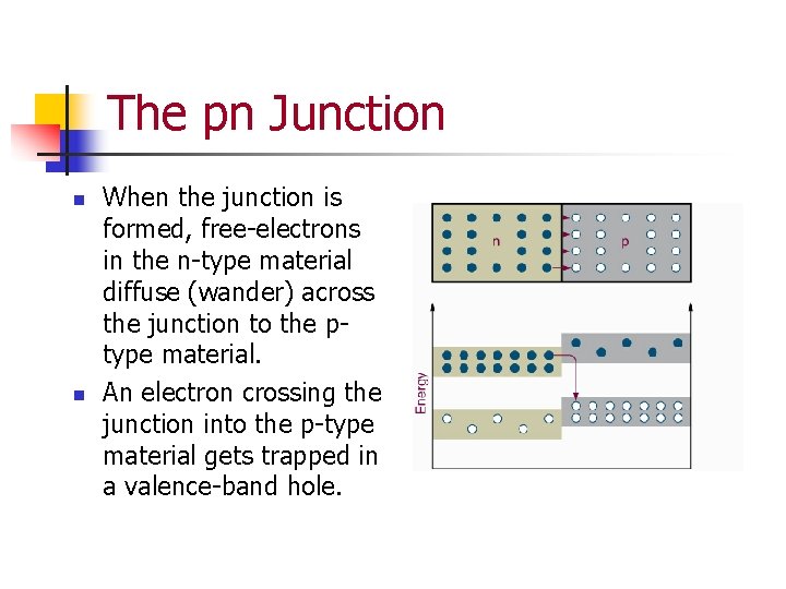
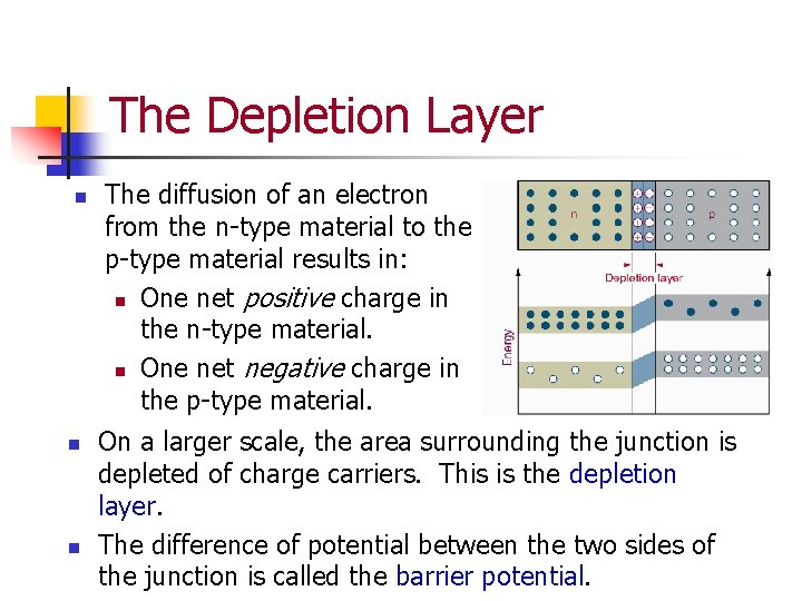
The pn Junction n n When the junction is formed, free-electrons in the n-type material diffuse (wander) across the junction to the ptype material. An electron crossing the junction into the p-type material gets trapped in a valence-band hole.

The Depletion Layer n n n The diffusion of an electron from the n-type material to the p-type material results in: n One net positive charge in the n-type material. n One net negative charge in the p-type material. On a larger scale, the area surrounding the junction is depleted of charge carriers. This is the depletion layer. The difference of potential between the two sides of the junction is called the barrier potential.

Bias A potential applied to a pn junction to obtain a desired mode of operation. n Forward bias – A potential used to reduce the resistance of a pn junction. n Reverse bias – A potential used to increase the resistance of a pn junction.

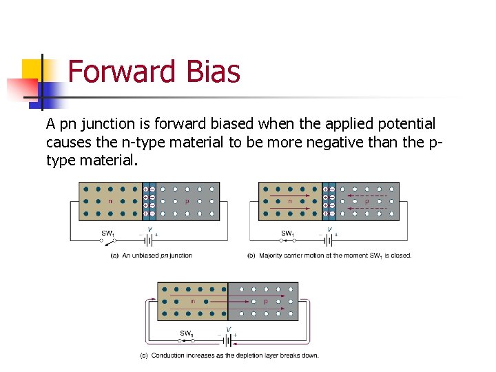
Forward Bias A pn junction is forward biased when the applied potential causes the n-type material to be more negative than the ptype material.

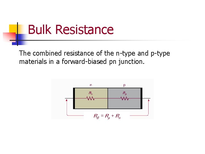
Bulk Resistance The combined resistance of the n-type and p-type materials in a forward-biased pn junction. RB = Rp + Rn

Forward Voltage n n Forward voltage (VF) is the voltage across a forward biased pn junction. VF is greater than the junction barrier potential. VF 0. 7 V (for silicon) VF 0. 3 V (for germanium) n Any differences between the measured and approximated values of VF result primarily from the current through the diode bulk resistance.

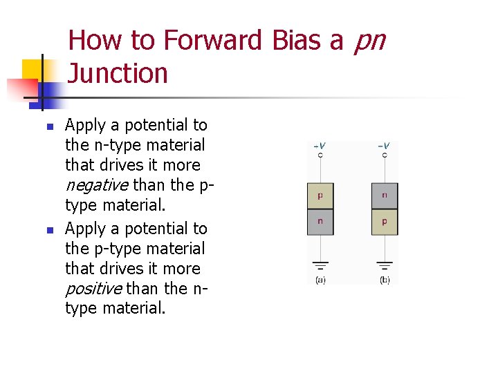
How to Forward Bias a pn Junction n n Apply a potential to the n-type material that drives it more negative than the ptype material. Apply a potential to the p-type material that drives it more positive than the ntype material.

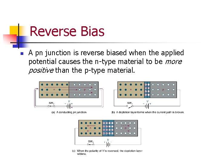
Reverse Bias n A pn junction is reverse biased when the applied potential causes the n-type material to be more positive than the p-type material.

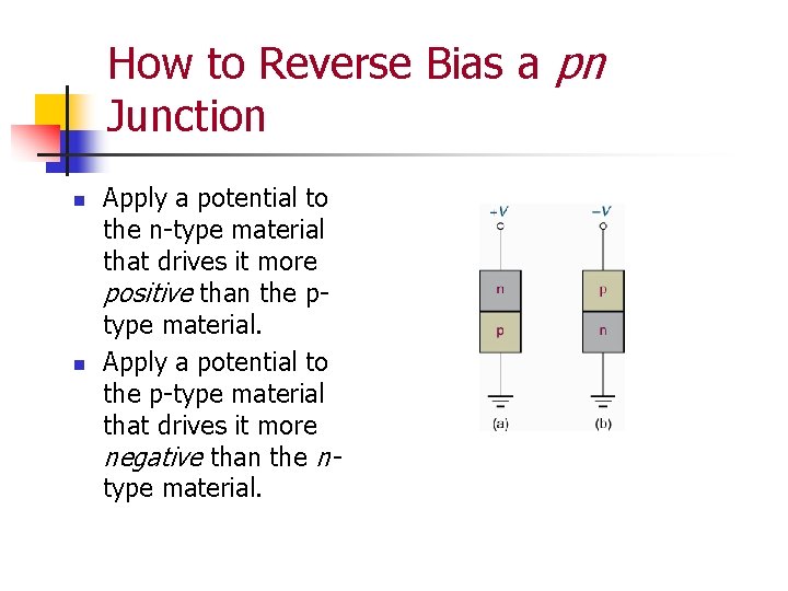
How to Reverse Bias a pn Junction n n Apply a potential to the n-type material that drives it more positive than the ptype material. Apply a potential to the p-type material that drives it more negative than the ntype material.

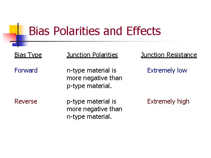
Bias Polarities and Effects Bias Type Junction Polarities Junction Resistance Forward n-type material is more negative than p-type material. Extremely low Reverse p-type material is more negative than n-type material. Extremely high