Outcome from the VMMs TGC Workshop at Weizmann

- Slides: 48

Outcome from the VMM/s. TGC Workshop at Weizmann Institute May 14 -15, 2015 Gianluigi De Geronimo Brookhaven National Laboratory, Upton, NY Acknowledgement Brigitte Vachon, Vladimir Smakhtin, Alex Vdovin, Nachman Lupu, Benoit Lefebvre, George Mikenberg, Lorne Levinson, Daniel Lellouch, Venetios Polychronakos 1 May 22 nd, 2015

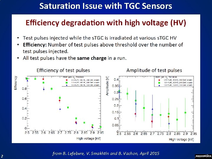
Saturation Issue with TGC Sensors 2 from B. Lefebvre, V. Smakhtin and B. Vachon, April 2015

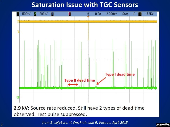
Saturation Issue with TGC Sensors 3 from B. Lefebvre, V. Smakhtin and B. Vachon, April 2015

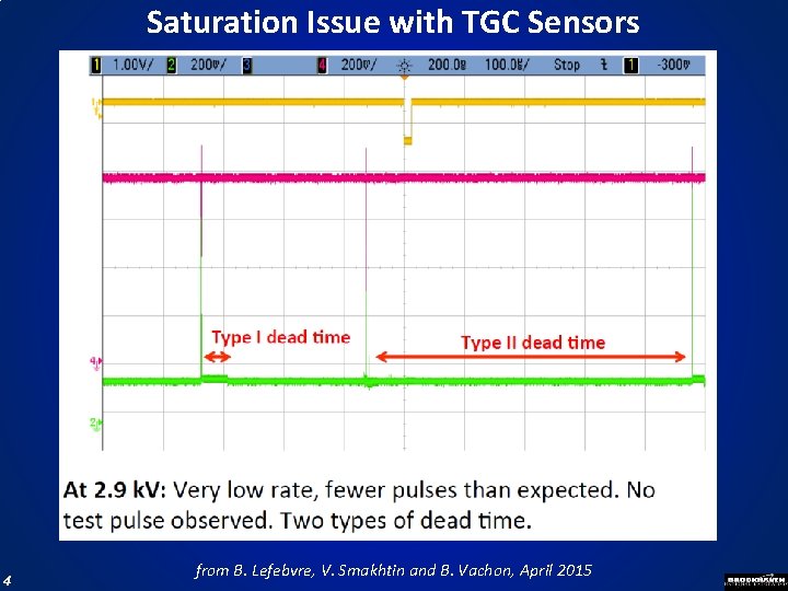
Saturation Issue with TGC Sensors 4 from B. Lefebvre, V. Smakhtin and B. Vachon, April 2015

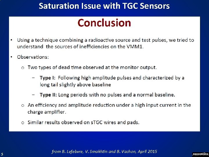
Saturation Issue with TGC Sensors 5 from B. Lefebvre, V. Smakhtin and B. Vachon, April 2015

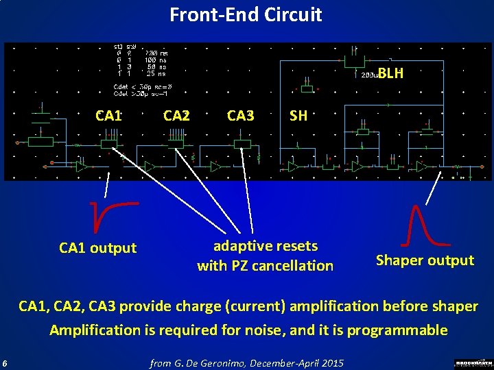
Front-End Circuit BLH CA 1 output CA 2 CA 3 SH adaptive resets with PZ cancellation Shaper output CA 1, CA 2, CA 3 provide charge (current) amplification before shaper Amplification is required for noise, and it is programmable 6 from G. De Geronimo, December-April 2015

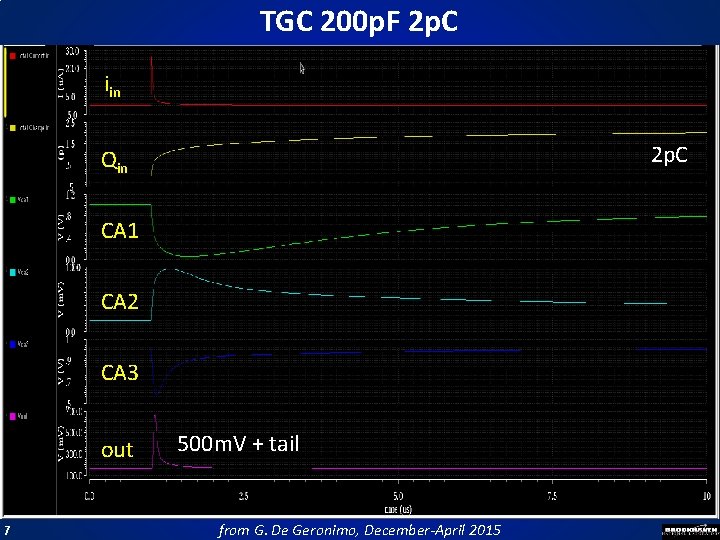
TGC 200 p. F 2 p. C iin 2 p. C Qin CA 1 CA 2 CA 3 out 7 500 m. V + tail from G. De Geronimo, December-April 2015

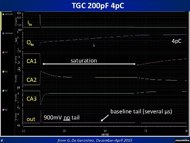
TGC 200 p. F 4 p. C iin 4 p. C Qin CA 1 saturation CA 2 CA 3 out 8 900 m. V no tail baseline tail (several µs) from G. De Geronimo, December-April 2015

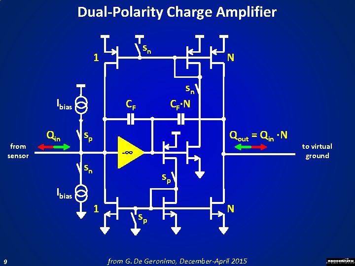
Dual-Polarity Charge Amplifier sn 1 Ibias from sensor Qin sn CF·N CF sp Qout = Qin ·N -∞ sn sp Ibias 1 9 N sp N from G. De Geronimo, December-April 2015 to virtual ground

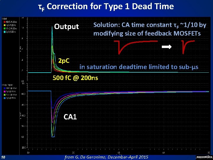
τF Correction for Type 1 Dead Time Output 2 p. C Solution: CA time constant τF ~1/10 by modifying size of feedback MOSFETs in saturation deadtime limited to sub-µs 500 f. C @ 200 ns CA 1 10 from G. De Geronimo, December-April 2015

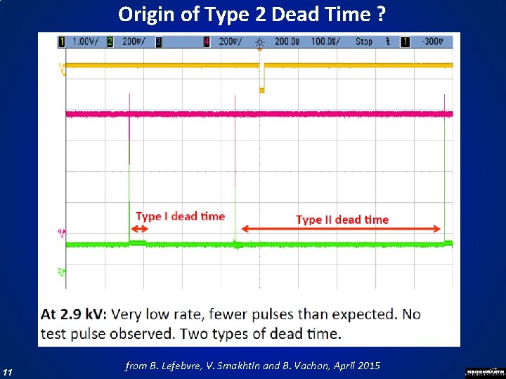
Origin of Type 2 Dead Time ? 11 from B. Lefebvre, V. Smakhtin and B. Vachon, April 2015

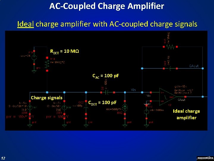
AC-Coupled Charge Amplifier Ideal charge amplifier with AC-coupled charge signals RDET = 10 MΩ CAC = 100 p. F Charge signals CDET = 100 p. F Ideal charge amplifier 12

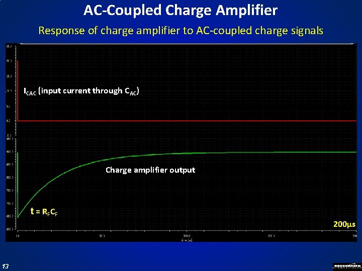
AC-Coupled Charge Amplifier Response of charge amplifier to AC-coupled charge signals ICAC (input current through CAC) Charge amplifier output t = R F CF 200µs 13

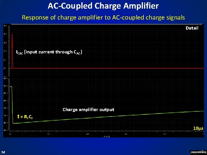
AC-Coupled Charge Amplifier Response of charge amplifier to AC-coupled charge signals Detail ICAC (input current through CAC) Charge amplifier output t = R F CF 10µs 14

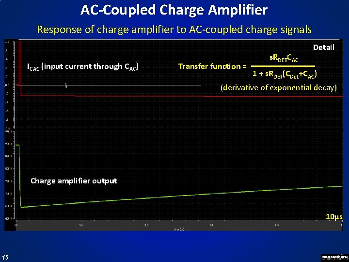
AC-Coupled Charge Amplifier Response of charge amplifier to AC-coupled charge signals ICAC (input current through CAC) Transfer function = s. RDETCAC Detail 1 + s. RDET(CDet+CAC) (derivative of exponential decay) Charge amplifier output 10µs 15

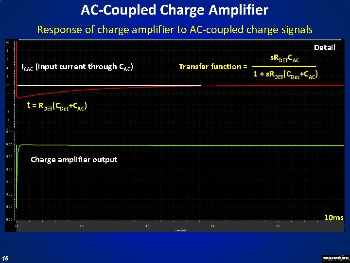
AC-Coupled Charge Amplifier Response of charge amplifier to AC-coupled charge signals ICAC (input current through CAC) Transfer function = s. RDETCAC Detail 1 + s. RDET(CDet+CAC) t = RDET(CDet+CAC) Charge amplifier output 10 ms 16

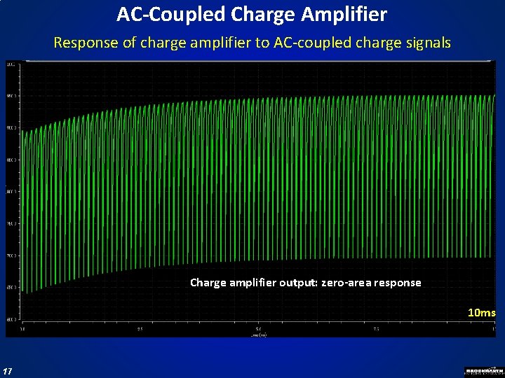
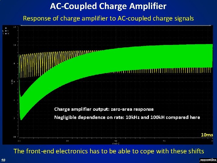
AC-Coupled Charge Amplifier Response of charge amplifier to AC-coupled charge signals Charge amplifier output: zero-area response 10 ms 17

AC-Coupled Charge Amplifier Response of charge amplifier to AC-coupled charge signals Charge amplifier output: zero-area response Negligible dependence on rate: 10 k. Hz and 100 k. H compared here 10 ms The front-end electronics has to be able to cope with these shifts 18

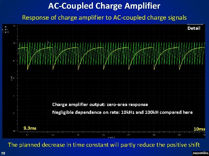
AC-Coupled Charge Amplifier Response of charge amplifier to AC-coupled charge signals Detail Charge amplifier output: zero-area response Negligible dependence on rate: 10 k. Hz and 100 k. H compared here 9. 3 ms 10 ms The planned decrease in time constant will partly reduce the positive shift 19

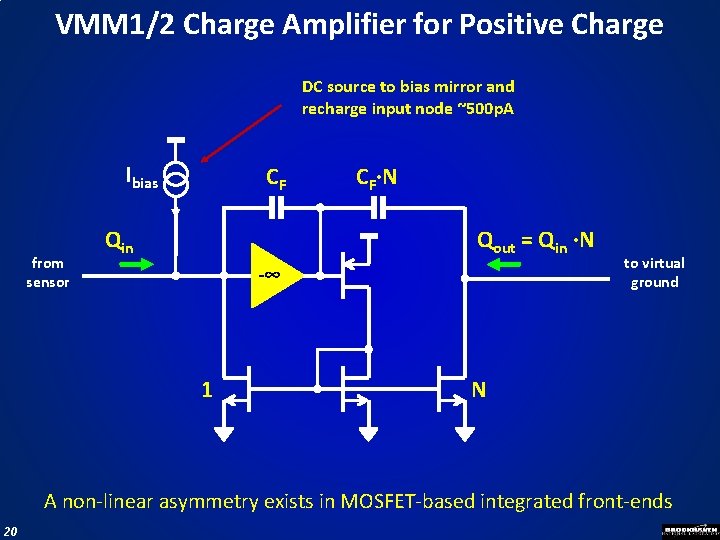
VMM 1/2 Charge Amplifier for Positive Charge DC source to bias mirror and recharge input node ~500 p. A Ibias from sensor CF Qin CF·N Qout = Qin ·N -∞ 1 to virtual ground N A non-linear asymmetry exists in MOSFET-based integrated front-ends 20

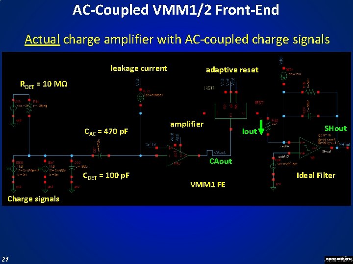
AC-Coupled VMM 1/2 Front-End Actual charge amplifier with AC-coupled charge signals leakage current adaptive reset RDET = 10 MΩ CAC = 470 p. F amplifier Iout SHout CAout CDET = 100 p. F Charge signals 21 VMM 1 FE Ideal Filter

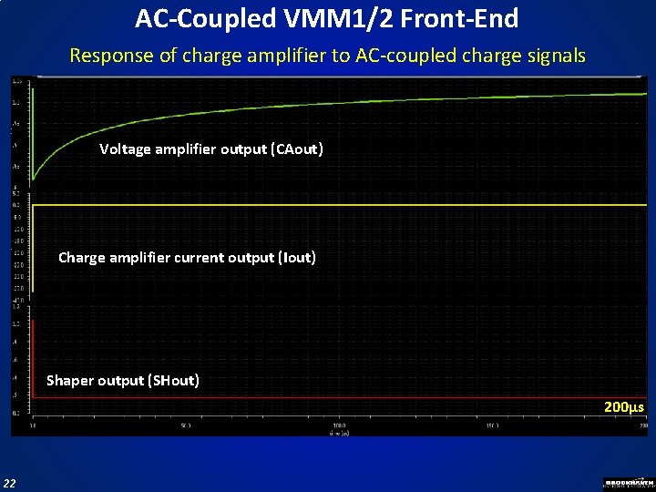
AC-Coupled VMM 1/2 Front-End Response of charge amplifier to AC-coupled charge signals Voltage amplifier output (CAout) Charge amplifier current output (Iout) Shaper output (SHout) 200µs 22

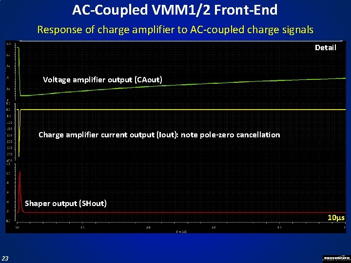
AC-Coupled VMM 1/2 Front-End Response of charge amplifier to AC-coupled charge signals Detail Voltage amplifier output (CAout) Charge amplifier current output (Iout): note pole-zero cancellation Shaper output (SHout) 10µs 23

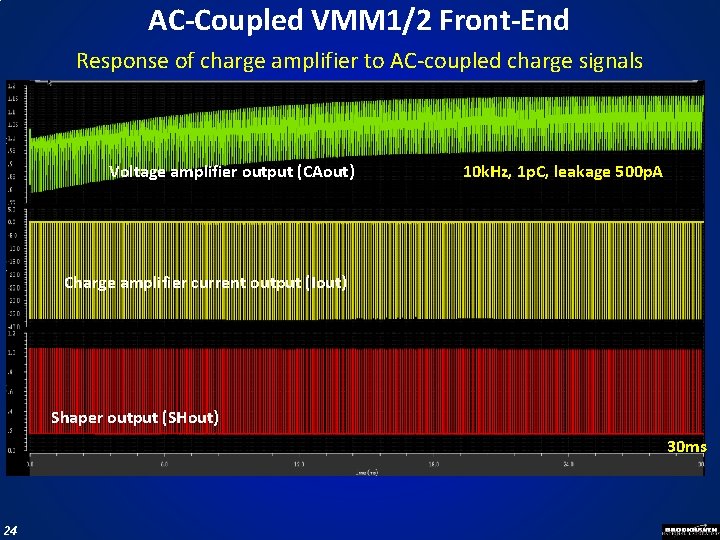
AC-Coupled VMM 1/2 Front-End Response of charge amplifier to AC-coupled charge signals Voltage amplifier output (CAout) 10 k. Hz, 1 p. C, leakage 500 p. A Charge amplifier current output (Iout) Shaper output (SHout) 30 ms 24

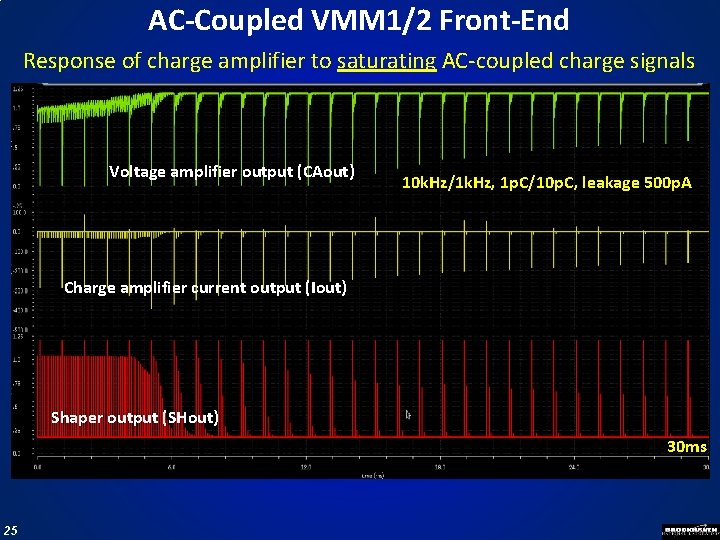
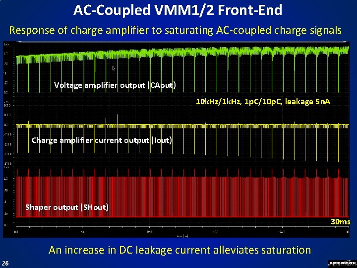
AC-Coupled VMM 1/2 Front-End Response of charge amplifier to saturating AC-coupled charge signals Voltage amplifier output (CAout) 10 k. Hz/1 k. Hz, 1 p. C/10 p. C, leakage 500 p. A Charge amplifier current output (Iout) Shaper output (SHout) 30 ms 25

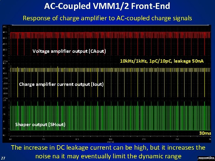
AC-Coupled VMM 1/2 Front-End Response of charge amplifier to saturating AC-coupled charge signals Voltage amplifier output (CAout) 10 k. Hz/1 k. Hz, 1 p. C/10 p. C, leakage 5 n. A Charge amplifier current output (Iout) Shaper output (SHout) 30 ms An increase in DC leakage current alleviates saturation 26

AC-Coupled VMM 1/2 Front-End Response of charge amplifier to AC-coupled charge signals Voltage amplifier output (CAout) 10 k. Hz/1 k. Hz, 1 p. C/10 p. C, leakage 50 n. A Charge amplifier current output (Iout) Shaper output (SHout) 30 ms 27 The increase in DC leakage current can be high, but it increases the noise na it may eventually limit the dynamic range

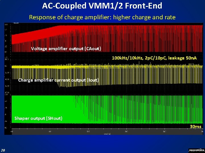
AC-Coupled VMM 1/2 Front-End Response of charge amplifier: higher charge and rate Voltage amplifier output (CAout) 100 k. Hz/10 k. Hz, 2 p. C/10 p. C, leakage 50 n. A Charge amplifier current output (Iout) Shaper output (SHout) 30 ms 28

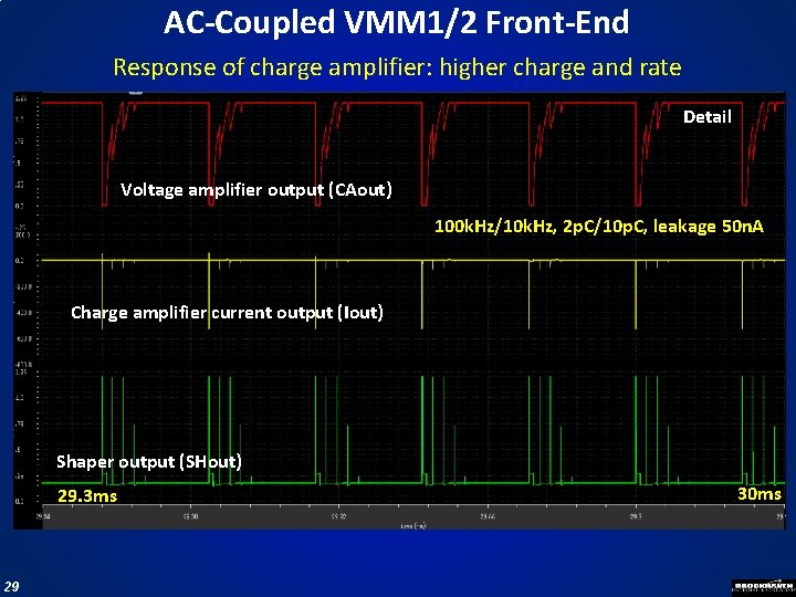
AC-Coupled VMM 1/2 Front-End Response of charge amplifier: higher charge and rate Detail Voltage amplifier output (CAout) 100 k. Hz/10 k. Hz, 2 p. C/10 p. C, leakage 50 n. A Charge amplifier current output (Iout) Shaper output (SHout) 29. 3 ms 29 30 ms

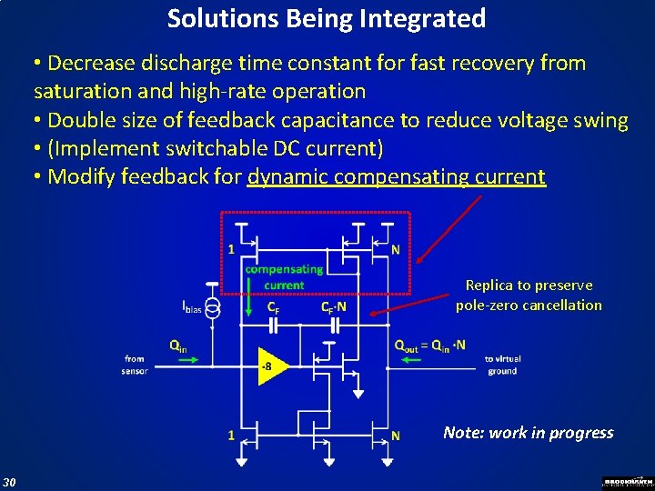
Solutions Being Integrated • Decrease discharge time constant for fast recovery from saturation and high-rate operation • Double size of feedback capacitance to reduce voltage swing • (Implement switchable DC current) • Modify feedback for dynamic compensating current Replica to preserve pole-zero cancellation Note: work in progress 30

Description of experimental setup and observations made at the Weizmann Institute on 15 May 2015. 1) Readout of small s. TGC prototype strips 2) Readout of Module-1 s. TGC pad 31 from Brigitte Vachon and Vladimir Smakhtin, May 2015

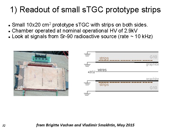
1) Readout of small s. TGC prototype strips Small 10 x 20 cm 2 prototype s. TGC with strips on both sides. Chamber operated at nominal operational HV of 2. 9 k. V Look at signals from Sr-90 radioactive source (rate ~ 10 k. Hz) strips G 10 graphite +HV wires graphite strips 32 from Brigitte Vachon and Vladimir Smakhtin, May 2015 G 10

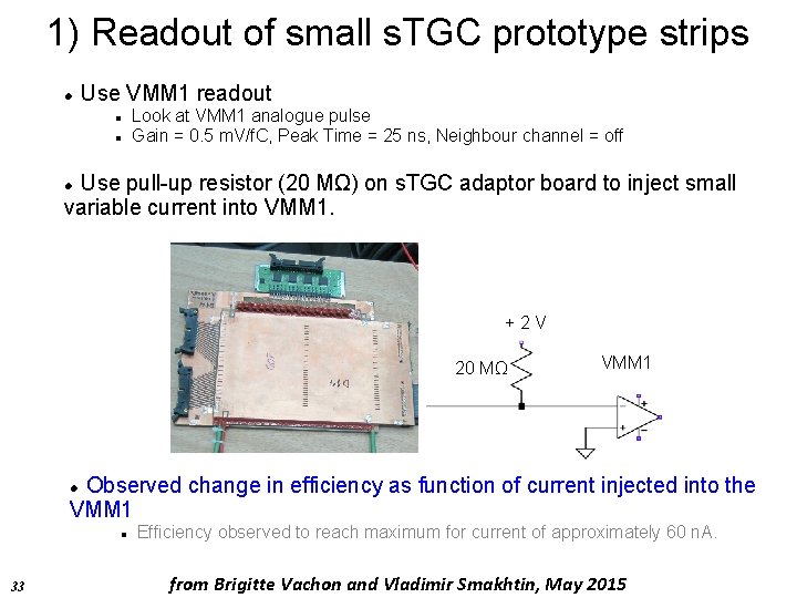
1) Readout of small s. TGC prototype strips Use VMM 1 readout Look at VMM 1 analogue pulse Gain = 0. 5 m. V/f. C, Peak Time = 25 ns, Neighbour channel = off Use pull-up resistor (20 MΩ) on s. TGC adaptor board to inject small variable current into VMM 1. +2 V 20 MΩ VMM 1 Observed change in efficiency as function of current injected into the VMM 1 33 Efficiency observed to reach maximum for current of approximately 60 n. A. from Brigitte Vachon and Vladimir Smakhtin, May 2015

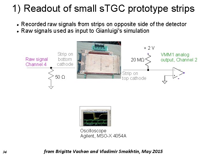
1) Readout of small s. TGC prototype strips Recorded raw signals from strips on opposite side of the detector Raw signals used as input to Gianluigi's simulation +2 V Raw signal Channel 4 Strip on bottom cathode 50 Ω 20 MΩ VMM 1 analog output, Channel 2 Strip on top cathode Oscilloscope Agilent, MSO-X 4054 A 34 from Brigitte Vachon and Vladimir Smakhtin, May 2015

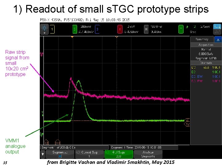
1) Readout of small s. TGC prototype strips Raw strip signal from small 10 x 20 cm 2 prototype VMM 1 analogue output 35 35 from Brigitte Vachon and Vladimir Smakhtin, May 2015

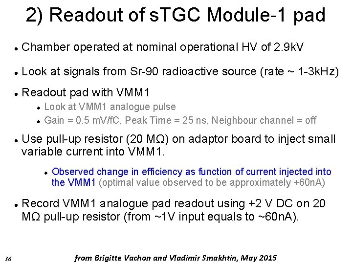
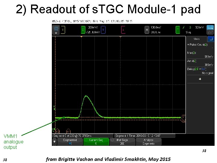
2) Readout of s. TGC Module-1 pad Chamber operated at nominal operational HV of 2. 9 k. V Look at signals from Sr-90 radioactive source (rate ~ 1 -3 k. Hz) Readout pad with VMM 1 Look at VMM 1 analogue pulse Gain = 0. 5 m. V/f. C, Peak Time = 25 ns, Neighbour channel = off Use pull-up resistor (20 MΩ) on adaptor board to inject small variable current into VMM 1. 36 Observed change in efficiency as function of current injected into the VMM 1 (optimal value observed to be approximately +60 n. A) Record VMM 1 analogue pad readout using +2 V DC on 20 MΩ pull-up resistor (from ~1 V input equals to ~60 n. A). from Brigitte Vachon and Vladimir Smakhtin, May 2015

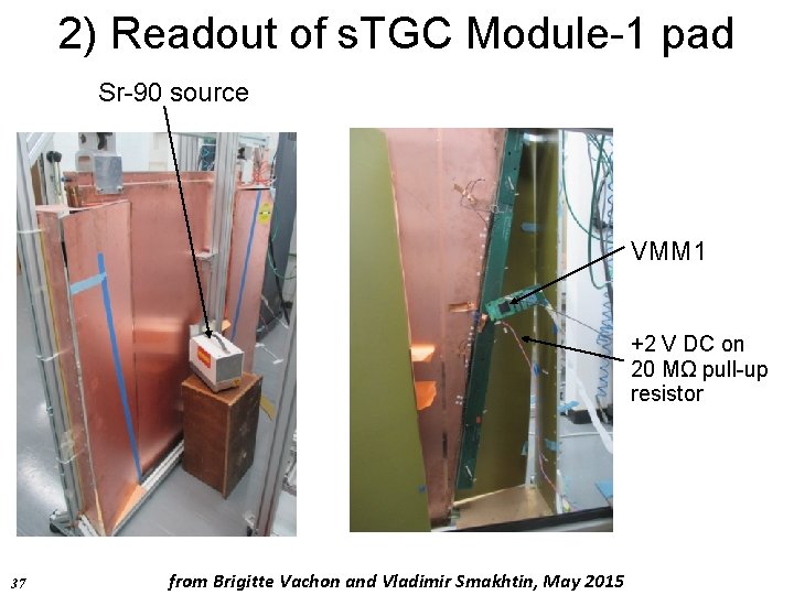
2) Readout of s. TGC Module-1 pad Sr-90 source VMM 1 +2 V DC on 20 MΩ pull-up resistor 37 from Brigitte Vachon and Vladimir Smakhtin, May 2015

2) Readout of s. TGC Module-1 pad VMM 1 analogue output 38 38 from Brigitte Vachon and Vladimir Smakhtin, May 2015

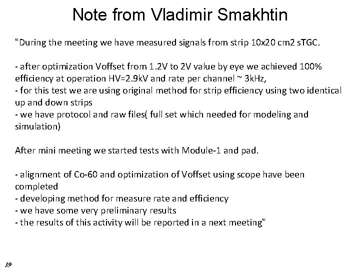
Note from Vladimir Smakhtin "During the meeting we have measured signals from strip 10 x 20 cm 2 s. TGC. - after optimization Voffset from 1. 2 V to 2 V value by eye we achieved 100% efficiency at operation HV=2. 9 k. V and rate per channel ~ 3 k. Hz, - for this test we are using original method for strip efficiency using two identical up and down strips - we have protocol and raw files( full set which needed for modeling and simulation) After mini meeting we started tests with Module-1 and pad. - alignment of Co-60 and optimization of Voffset using scope have been completed - developing method for measure rate and efficiency - we have some very preliminary results - the results of this activity will be reported in a next meeting" 39

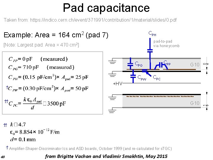
Pad capacitance Taken from: https: //indico. cern. ch/event/371991/contribution/1/material/slides/0. pdf CPH Example: Area = 164 cm 2 (pad 7) pad-to-pad via honeycomb [Note: Largest pad: Area = 470 cm 2] CPP CPG CPW ϯ CPC +HV ϯϯ G 10 ϯϯ ϯ Amplifier-Shaper-Discriminator Ics and ASD boards, October 1999 (and re-calculated for s. TGC) 40 G 10 from Brigitte Vachon and Vladimir Smakhtin, May 2015

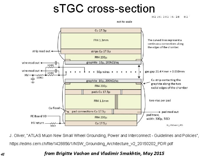
s. TGC cross-section J. Oliver, “ATLAS Muon New Small Wheel Grounding, Power and Interconnect - Guidelines and Policies”, https: //edms. cern. ch/file/1428856/1/NSW_Grounding_Architecture_v 2_20150202_PDR. pdf 41 from Brigitte Vachon and Vladimir Smakhtin, May 2015

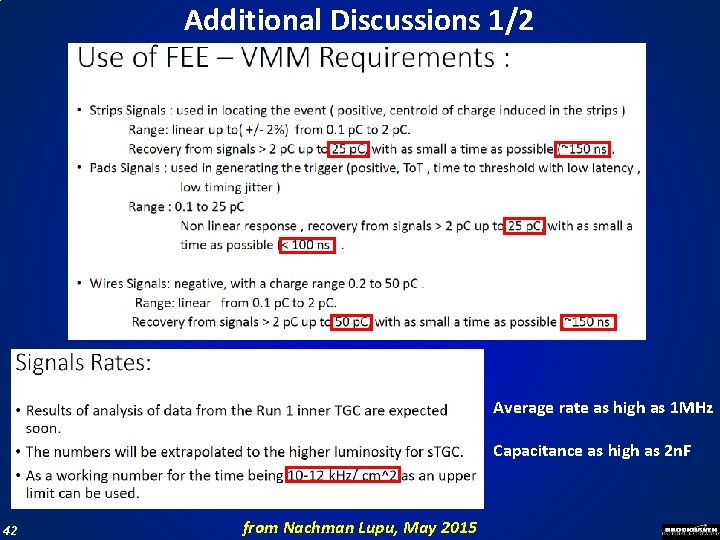
Additional Discussions 1/2 Average rate as high as 1 MHz Capacitance as high as 2 n. F 42 from Nachman Lupu, May 2015

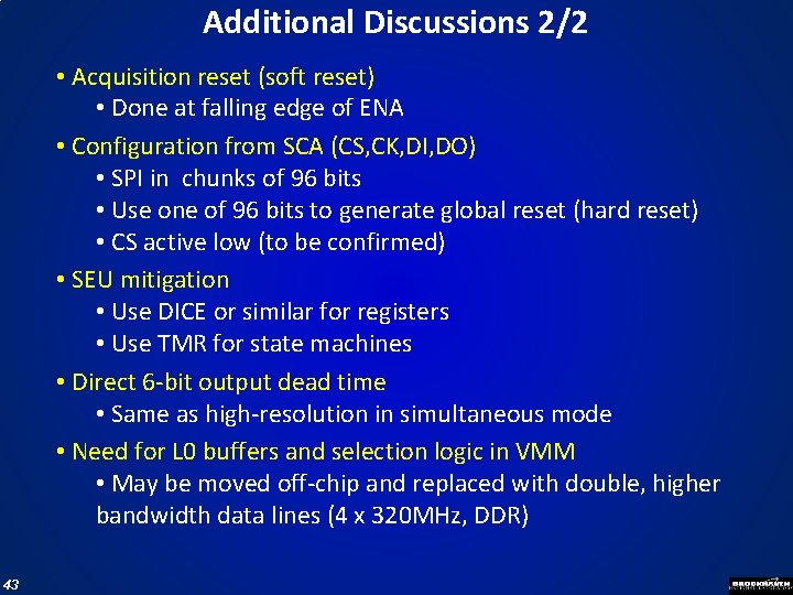
Additional Discussions 2/2 • Acquisition reset (soft reset) • Done at falling edge of ENA • Configuration from SCA (CS, CK, DI, DO) • SPI in chunks of 96 bits • Use one of 96 bits to generate global reset (hard reset) • CS active low (to be confirmed) • SEU mitigation • Use DICE or similar for registers • Use TMR for state machines • Direct 6 -bit output dead time • Same as high-resolution in simultaneous mode • Need for L 0 buffers and selection logic in VMM • May be moved off-chip and replaced with double, higher bandwidth data lines (4 x 320 MHz, DDR) 43

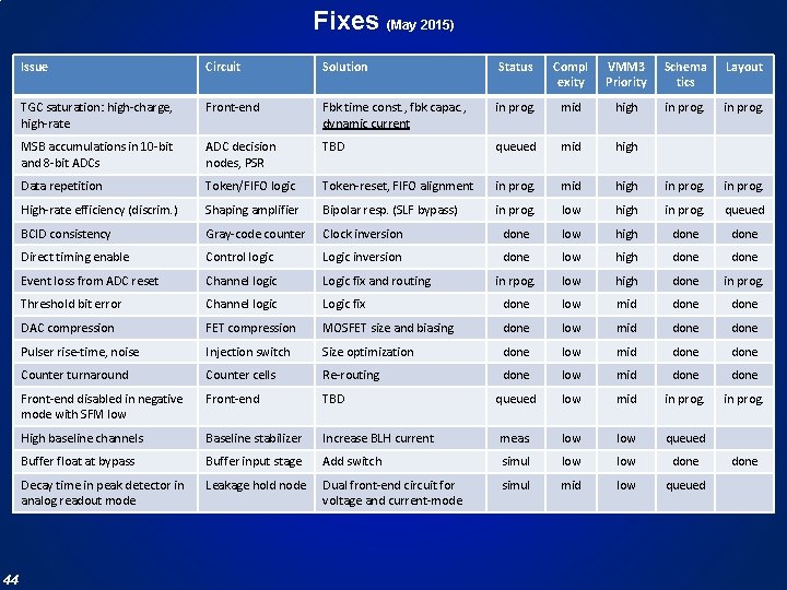
Fixes (May 2015) 44 Issue Circuit Solution Status Compl exity VMM 3 Priority Schema tics Layout TGC saturation: high-charge, high-rate Front-end Fbk time const. , fbk capac. , dynamic current in prog. mid high in prog. MSB accumulations in 10 -bit and 8 -bit ADCs ADC decision nodes, PSR TBD queued mid high Data repetition Token/FIFO logic Token-reset, FIFO alignment in prog. mid high in prog. High-rate efficiency (discrim. ) Shaping amplifier Bipolar resp. (SLF bypass) in prog. low high in prog. queued BCID consistency Gray-code counter Clock inversion done low high done Direct timing enable Control logic Logic inversion done low high done Event loss from ADC reset Channel logic Logic fix and routing in rpog. low high done in prog. Threshold bit error Channel logic Logic fix done low mid done DAC compression FET compression MOSFET size and biasing done low mid done Pulser rise-time, noise Injection switch Size optimization done low mid done Counter turnaround Counter cells Re-routing done low mid done Front-end disabled in negative mode with SFM low Front-end TBD queued low mid in prog. High baseline channels Baseline stabilizer Increase BLH current meas. low queued Buffer float at bypass Buffer input stage Add switch simul low done Decay time in peak detector in analog readout mode Leakage hold node Dual front-end circuit for voltage and current-mode simul mid low queued done

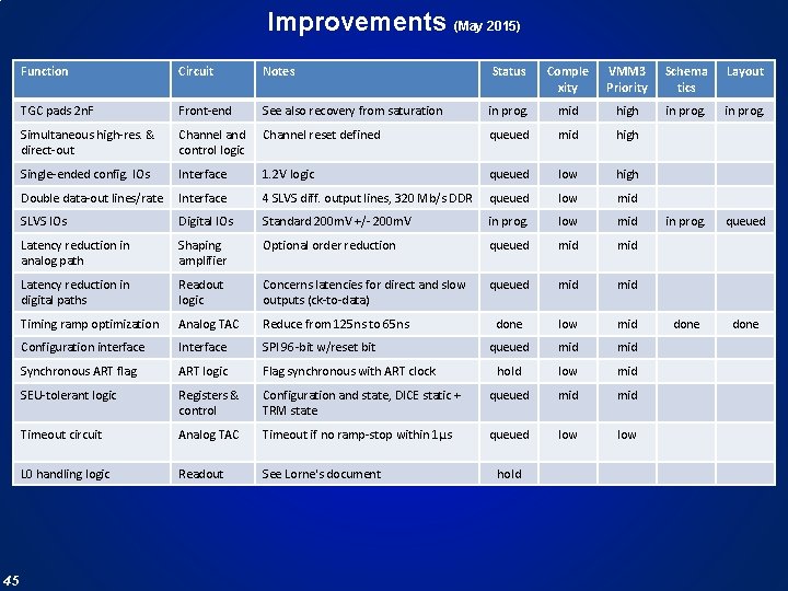
Improvements (May 2015) 45 Function Circuit Notes Status Comple xity VMM 3 Priority Schema tics Layout TGC pads 2 n. F Front-end See also recovery from saturation in prog. mid high in prog. Simultaneous high-res. & direct-out Channel and control logic Channel reset defined queued mid high Single-ended config. IOs Interface 1. 2 V logic queued low high Double data-out lines/rate Interface 4 SLVS diff. output lines, 320 Mb/s DDR queued low mid SLVS IOs Digital IOs Standard 200 m. V +/- 200 m. V in prog. low mid in prog. queued Latency reduction in analog path Shaping amplifier Optional order reduction queued mid Latency reduction in digital paths Readout logic Concerns latencies for direct and slow outputs (ck-to-data) queued mid Timing ramp optimization Analog TAC Reduce from 125 ns to 65 ns done low mid done Configuration interface Interface SPI 96 -bit w/reset bit queued mid Synchronous ART flag ART logic Flag synchronous with ART clock hold low mid SEU-tolerant logic Registers & control Configuration and state, DICE static + TRM state queued mid Timeout circuit Analog TAC Timeout if no ramp-stop within 1µs queued low L 0 handling logic Readout See Lorne's document hold

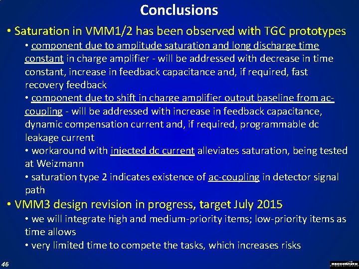
Conclusions • Saturation in VMM 1/2 has been observed with TGC prototypes • component due to amplitude saturation and long discharge time constant in charge amplifier - will be addressed with decrease in time constant, increase in feedback capacitance and, if required, fast recovery feedback • component due to shift in charge amplifier output baseline from accoupling - will be addressed with increase in feedback capacitance, dynamic compensation current and, if required, programmable dc leakage current • workaround with injected dc current alleviates saturation, being tested at Weizmann • saturation type 2 indicates existence of ac-coupling in detector signal path • VMM 3 design revision in progress, target July 2015 • we will integrate high and medium-priority items; low-priority items as time allows • very limited time to compete the tasks, which increases risks 46

Backup Slides 47

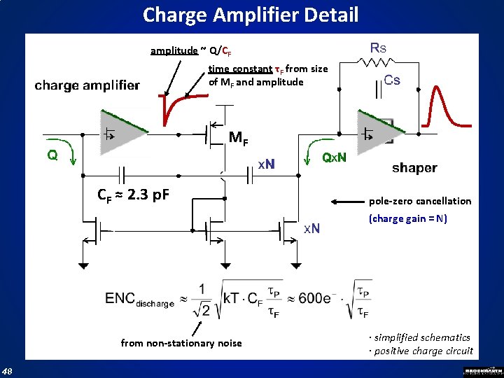
Charge Amplifier Detail amplitude ~ Q/CF time constant τF from size of MF and amplitude MF CF ≈ 2. 3 p. F pole-zero cancellation (charge gain = N) from non-stationary noise 48 · simplified schematics · positive charge circuit