Photovoltaics Fundamental concepts and novel systems First practical
- Slides: 46

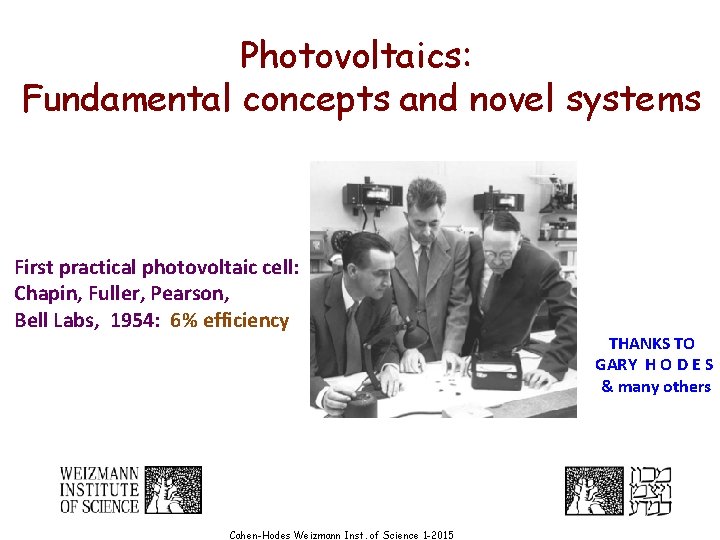
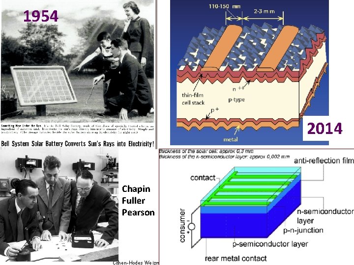
Photovoltaics: Fundamental concepts and novel systems First practical photovoltaic cell: Chapin, Fuller, Pearson, Bell Labs, 1954: 6% efficiency Cahen-Hodes Weizmann Inst. of Science 1 -2015 THANKS TO GARY H O D E S & many others

Outline • • • Energy levels bands Doping of semiconductors Energy band alignments between different phases Space charge layers p-n junctions, Schottky barriers p-n cells, Si cells, thin film cells Schottky cells (solid and liquid junction) p-i-n cells Fundamental limits of photovoltaic cells How to overcome/ bypass these limits New generation cells (brief survey) PV stability, efficiencies and economics Cahen-Hodes Weizmann Inst. of Science 1 -2015

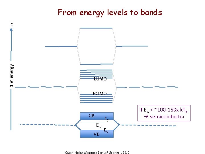
From energy levels to bands 1 e- energy E LUMO HOMO CB EG VB EC EV Cahen-Hodes Weizmann Inst. of Science 1 -2015 If EG < ~100 -150 x k. TB semiconductor

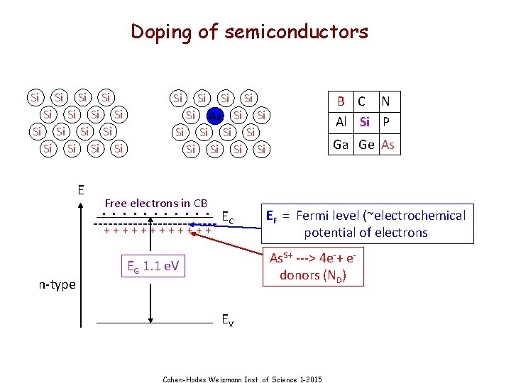
Doping of semiconductors Si Si Si Si As Si Si Si Si E Si Si Si Free electrons in CB ++++++ n-type EC B C N Al Si P Ga Ge As EF = Fermi level (~electrochemical potential of electrons As 5+ ---> 4 e-+ edonors (ND) EG 1. 1 e. V EV Cahen-Hodes Weizmann Inst. of Science 1 -2015

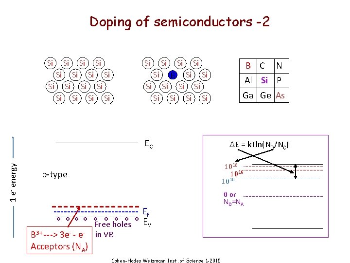
Doping of semiconductors -2 Si Si Si Si Si Si B Si Si B C N Al Si P Si Ga Ge As Si Si 1 e- energy EC 1018 1016 1010 p-type B 3+ ---> 3 e- - e. Acceptors (NA) DE = k. Tln(ND/NC) Free holes in VB EF EV Cahen-Hodes Weizmann Inst. of Science 1 -2015 0 or ND=NA

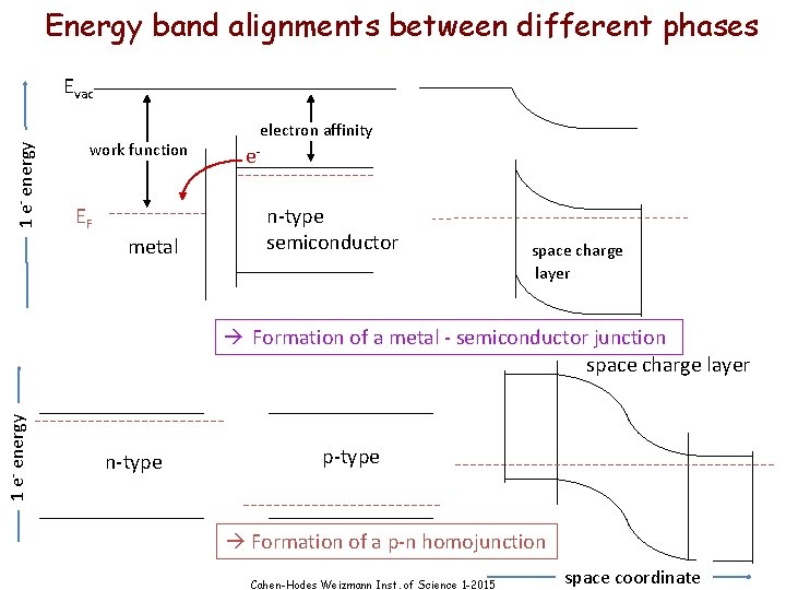
Energy band alignments between different phases 1 e- energy Evac work function EF metal electron affinity en-type semiconductor space charge layer 1 e- energy Formation of a metal - semiconductor junction space charge layer n-type p-type Formation of a p-n homojunction Cahen-Hodes Weizmann Inst. of Science 1 -2015 space coordinate

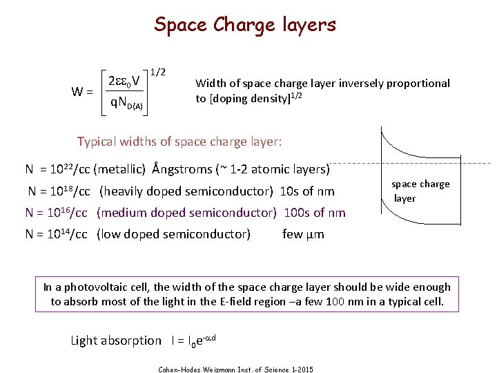
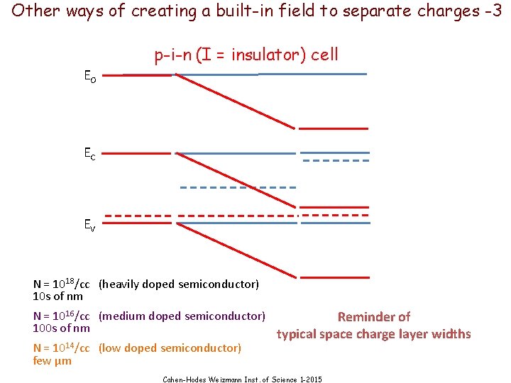
Space Charge layers W= 2 ee 0 V q. ND(A) 1/2 Width of space charge layer inversely proportional to [doping density]1/2 Typical widths of space charge layer: N = 1022/cc (metallic) Ångstroms (~ 1 -2 atomic layers) N = 1018/cc (heavily doped semiconductor) 10 s of nm N = 1016/cc (medium doped semiconductor) 100 s of nm N = 1014/cc (low doped semiconductor) space charge layer few µm In a photovoltaic cell, the width of the space charge layer should be wide enough to absorb most of the light in the E-field region –a few 100 nm in a typical cell. Light absorption I = I 0 e-ad Cahen-Hodes Weizmann Inst. of Science 1 -2015

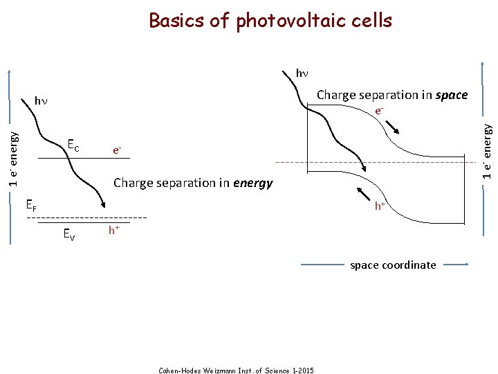
Basics of photovoltaic cells hn Charge separation in space e- EC 1 e- energy hn e- Charge separation in energy EF h+ EV h+ space coordinate Cahen-Hodes Weizmann Inst. of Science 1 -2015

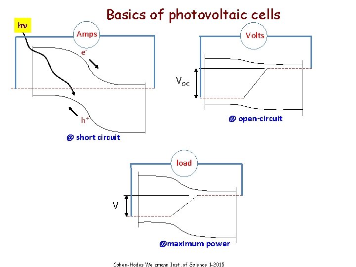
hn Basics of photovoltaic cells Amps Volts e- VOC @ open-circuit h+ @ short circuit load V @maximum power Cahen-Hodes Weizmann Inst. of Science 1 -2015

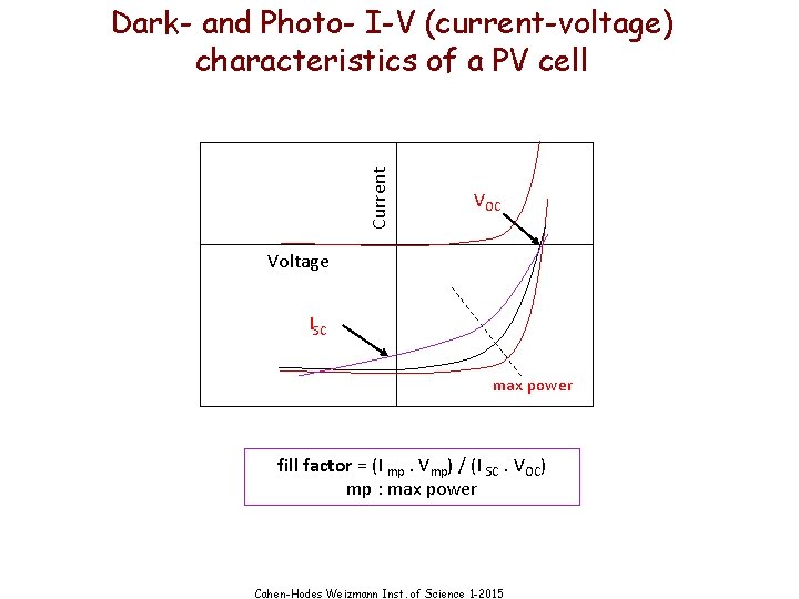
Current Dark- and Photo- I-V (current-voltage) characteristics of a PV cell VOC Voltage ISC max power fill factor = (I mp. Vmp) / (I SC. VOC) mp : max power Cahen-Hodes Weizmann Inst. of Science 1 -2015

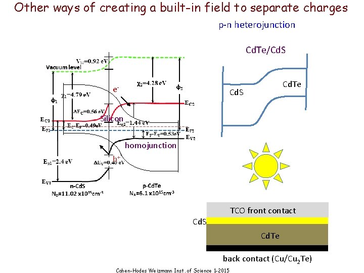
Other ways of creating a built-in field to separate charges p-n heterojunction Cd. Te/Cd. S e- Cd. Te Cd. S Silicon homojunction h+ TCO front contact Cd. S Cd. Te back contact (Cu/Cu 2 Te) Cahen-Hodes Weizmann Inst. of Science 1 -2015

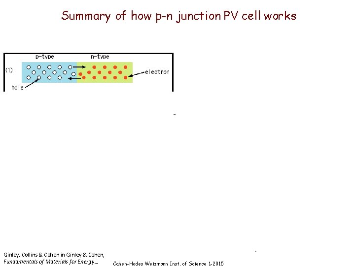
Summary of how p-n junction PV cell works 1 e- energy • Absorb light • Absorbed light creates carriers • Carrier collection, by diffusion, drift space Ginley, Collins & Cahen in Ginley & Cahen, Fundamentals of Materials for Energy… Cahen-Hodes Weizmann Inst. of Science 1 -2015

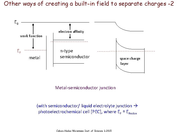
Other ways of creating a built-in field to separate charges -2 E 0 work function EF metal electron affinity n-type semiconductor space charge layer Metal-semiconductor junction (with semiconductor/ liquid electrolyte junction photoelectrochemical cell [PEC], where EF ≅ ERedox Cahen-Hodes Weizmann Inst. of Science 1 -2015

Other ways of creating a built-in field to separate charges -3 p-i-n (I = insulator) cell EO EC EV N = 1018/cc (heavily doped semiconductor) 10 s of nm N = 1016/cc (medium doped semiconductor) Reminder of 100 s of nm typical space charge layer widths 14 N = 10 /cc (low doped semiconductor) few µm Cahen-Hodes Weizmann Inst. of Science 1 -2015

1954 2014 Chapin Fuller Pearson Cahen-Hodes Weizmann Inst. of Science 1 -2015

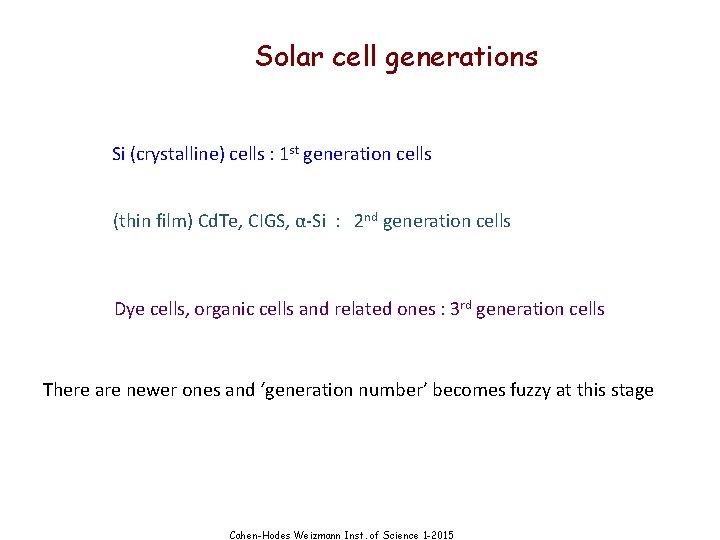
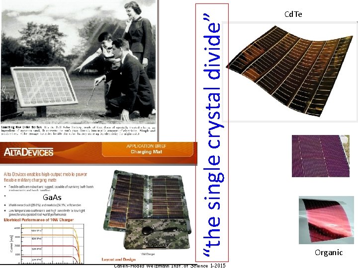
Solar cell generations Si (crystalline) cells : 1 st generation cells (thin film) Cd. Te, CIGS, α-Si : 2 nd generation cells Dye cells, organic cells and related ones : 3 rd generation cells There are newer ones and ‘generation number’ becomes fuzzy at this stage Cahen-Hodes Weizmann Inst. of Science 1 -2015

“the single crystal divide” Ga. As Cahen-Hodes Weizmann Inst. of Science 1 -2015 Cd. Te Organic

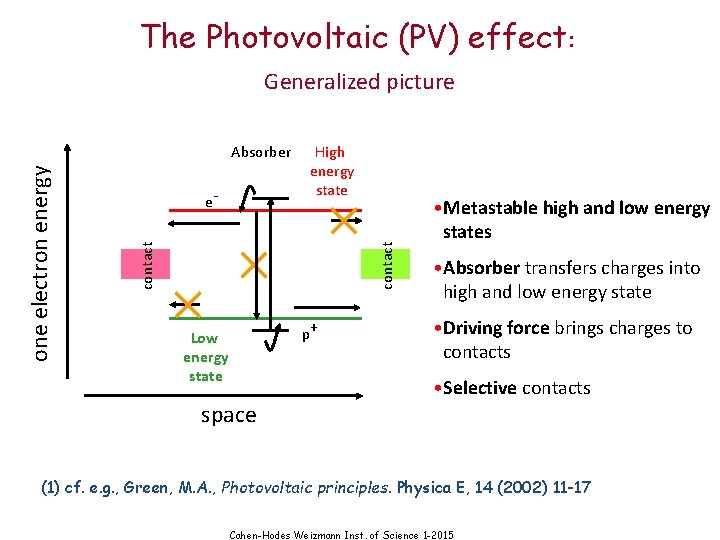
The Photovoltaic (PV) effect: Generalized picture contact e- High energy state contact one electron energy Absorber p+ Low energy state space • Metastable high and low energy states • Absorber transfers charges into high and low energy state • Driving force brings charges to contacts • Selective contacts (1) cf. e. g. , Green, M. A. , Photovoltaic principles. Physica E, 14 (2002) 11 -17 Cahen-Hodes Weizmann Inst. of Science 1 -2015

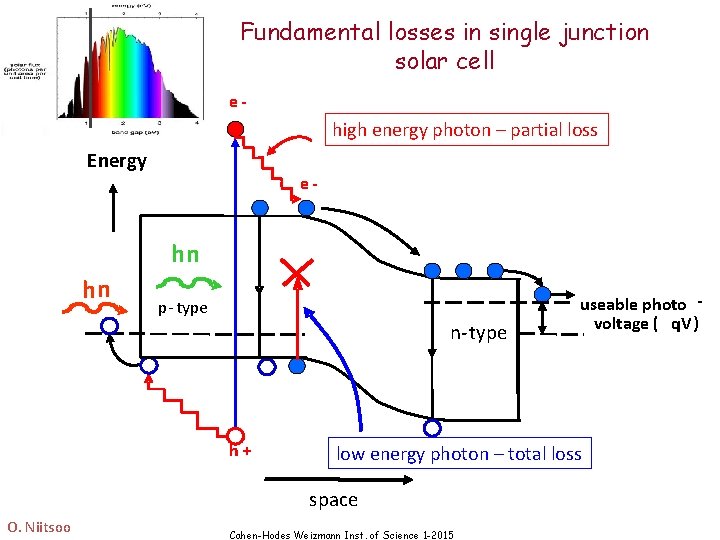
Fundamental losses in single junction solar cell e- high energy photon – partial loss Energy e- hn hn p- type n- type h+ low energy photon – total loss space O. Niitsoo useable photo voltage ( q. V) Cahen-Hodes Weizmann Inst. of Science 1 -2015

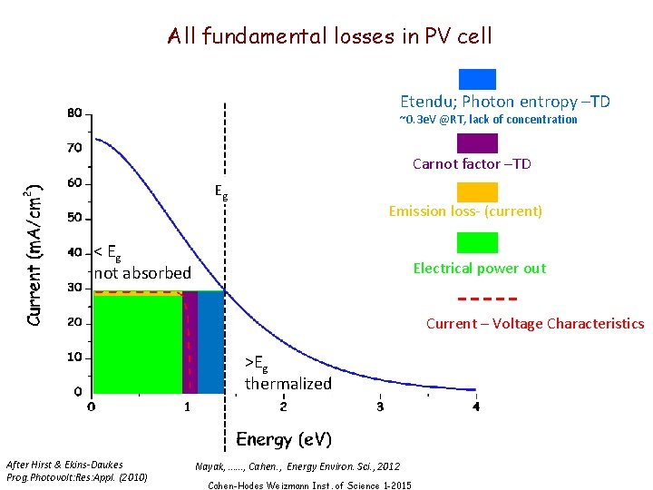
All fundamental losses in PV cell Etendu; Photon entropy –TD ~0. 3 e. V @RT, lack of concentration Carnot factor –TD Eg Emission loss- (current) < Eg not absorbed Electrical power out Current – Voltage Characteristics >Eg thermalized After Hirst & Ekins-Daukes Prog. Photovolt: Res: Appl. (2010) Nayak, ……, Cahen. , Energy Environ. Sci. , 2012 Cahen-Hodes Weizmann Inst. of Science 1 -2015

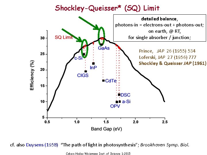
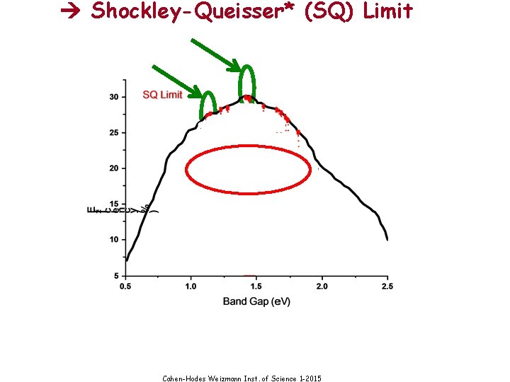
Shockley-Queisser* (SQ) Limit detailed balance, photons-in = electrons-out + photons-out; on earth, @ RT, for single absorber / junction; Prince, JAP 26 (1955) 534 Loferski, JAP 27 (1956) 777 Shockley & Queisser JAP (1961) cf. also Duysens (1958) “The path of light in photosynthesis”; Brookhaven Symp. Biol. Cahen-Hodes Weizmann Inst. of Science 1 -2015

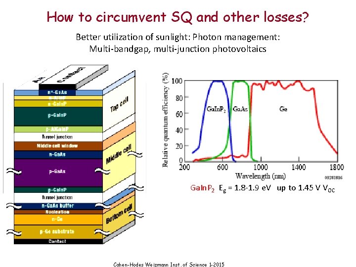
How to circumvent SQ and other losses? Better utilization of sunlight: Photon management: Multi-bandgap, multi-junction photovoltaics Ga. In. P 2 Eg = 1. 8 -1. 9 e. V up to 1. 45 V VOC Cahen-Hodes Weizmann Inst. of Science 1 -2015

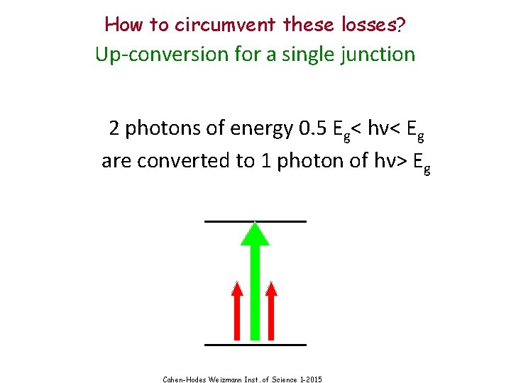
How to circumvent these losses? Up-conversion for a single junction 2 photons of energy 0. 5 Eg< hν< Eg are converted to 1 photon of hν> Eg Cahen-Hodes Weizmann Inst. of Science 1 -2015

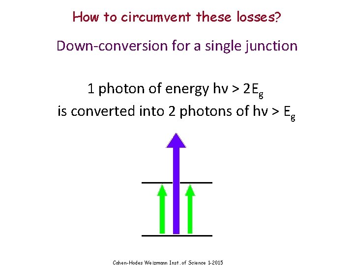
How to circumvent these losses? Down-conversion for a single junction 1 photon of energy hν > 2 Eg is converted into 2 photons of hν > Eg Cahen-Hodes Weizmann Inst. of Science 1 -2015

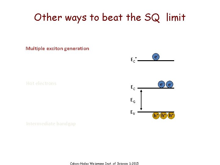
Other ways to beat the SQ limit Multiple exciton generation EC Hot electrons * EC e- e- e- EG EV Intermediate bandgap Cahen-Hodes Weizmann Inst. of Science 1 -2015 h+ h+ h+

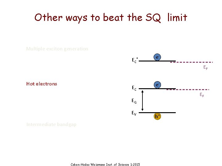
Other ways to beat the SQ limit Multiple exciton generation EC Hot electrons * EC e. EF EG EV Intermediate bandgap Cahen-Hodes Weizmann Inst. of Science 1 -2015 h+

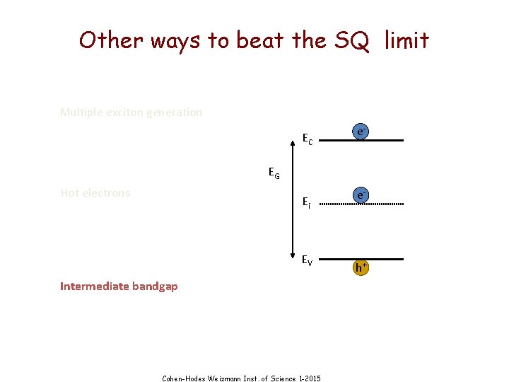
Other ways to beat the SQ limit Multiple exciton generation EC e- EG Hot electrons Ei EV Intermediate bandgap Cahen-Hodes Weizmann Inst. of Science 1 -2015 e- h+

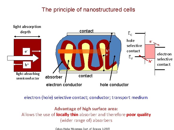
The principle of nanostructured cells light absorption depth contact EC h+ e- e- hole selective contact EV h+ light-absorbing semiconductor absorber e- h+ contact electron conductor hole conductor electron (hole) selective contact; conductor; transport medium Advantage of high surface area: Allows the use of locally thin absorber and therefore poor quality (wider range of) absorbers Cahen-Hodes Weizmann Inst. of Science 1 -2015 electron selective contact

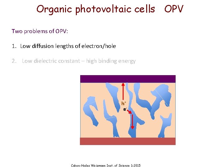
Organic photovoltaic cells OPV Two problems of OPV: 1. Low diffusion lengths of electron/hole 2. Low dielectric constant – high binding energy h+ e- Cahen-Hodes Weizmann Inst. of Science 1 -2015

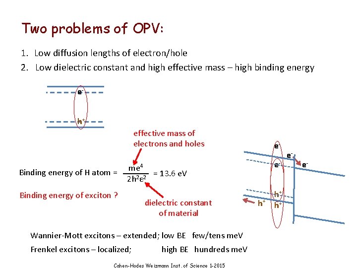
Two problems of OPV: 1. Low diffusion lengths of electron/hole 2. Low dielectric constant and high effective mass – high binding energy eh+ effective mass of electrons and holes Binding energy of H atom = ee- me 4 = 13. 6 e. V 2 h 2ε 2 Binding energy of exciton ? dielectric constant of material Wannier-Mott excitons – extended; low BE few/tens me. V Frenkel excitons – localized; high BE hundreds me. V Cahen-Hodes Weizmann Inst. of Science 1 -2015 h+ h+ h+ e- e-

Notwithstanding these problems, OPV is now at ~ 11% conversion efficiency Stability still not good enough for practical use, but improving Advantages: Cheap (in capital and in energy) Roll-to-roll manufacturing (large scale possible) Cahen-Hodes Weizmann Inst. of Science 1 -2015

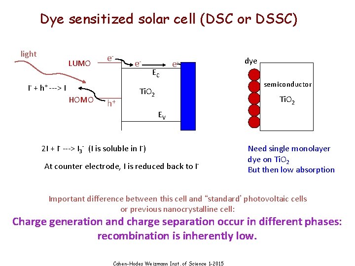
Dye sensitized solar cell (DSC or DSSC) light LUMO e- I- + h+ ---> I HOMO h+ e- EC e- dye semiconductor Ti. O 2 EV 2 I + I- ---> I 3 - (I is soluble in I-) At counter electrode, I is reduced back to I- Need single monolayer dye on Ti. O 2 But then low absorption Important difference between this cell and “standard’ photovoltaic cells or previous nanocrystalline cell: Charge generation and charge separation occur in different phases: recombination is inherently low. Cahen-Hodes Weizmann Inst. of Science 1 -2015

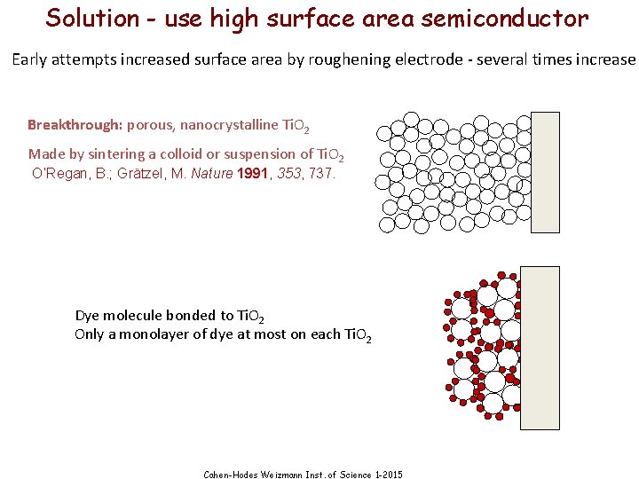
Solution - use high surface area semiconductor Early attempts increased surface area by roughening electrode - several times increase Breakthrough: porous, nanocrystalline Ti. O 2 Made by sintering a colloid or suspension of Ti. O 2 O’Regan, B. ; Grätzel, M. Nature 1991, 353, 737. Dye molecule bonded to Ti. O 2 Only a monolayer of dye at most on each Ti. O 2 Cahen-Hodes Weizmann Inst. of Science 1 -2015

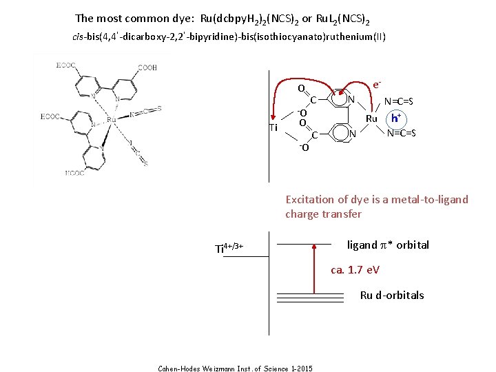
The most common dye: Ru(dcbpy. H 2)2(NCS)2 or Ru. L 2(NCS)2 cis-bis(4, 4’-dicarboxy-2, 2’-bipyridine)-bis(isothiocyanato)ruthenium(II) O -O Ti O -O e. C N N=C=S Ru C h+ N=C=S N Excitation of dye is a metal-to-ligand charge transfer Ti 4+/3+ ligand p* orbital ca. 1. 7 e. V Ru d-orbitals Cahen-Hodes Weizmann Inst. of Science 1 -2015

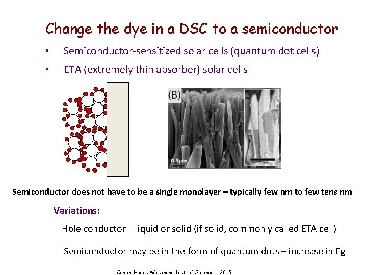
Change the dye in a DSC to a semiconductor • Semiconductor-sensitized solar cells (quantum dot cells) • ETA (extremely thin absorber) solar cells Semiconductor does not have to be a single monolayer – typically few nm to few tens nm Variations: Hole conductor – liquid or solid (if solid, commonly called ETA cell) Semiconductor may be in the form of quantum dots – increase in Eg Cahen-Hodes Weizmann Inst. of Science 1 -2015

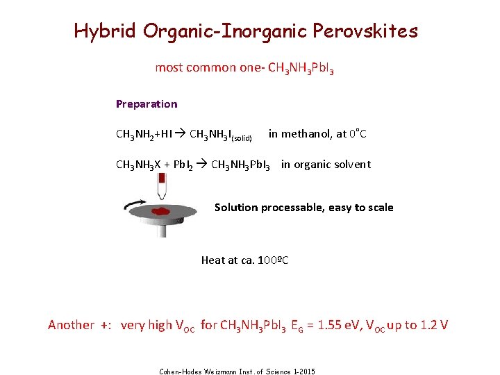
Hybrid Organic-Inorganic Perovskites most common one- CH 3 NH 3 Pb. I 3 Preparation CH 3 NH 2+HI CH 3 NH 3 I(solid) in methanol, at 0˚C CH 3 NH 3 X + Pb. I 2 CH 3 NH 3 Pb. I 3 in organic solvent Solution processable, easy to scale Heat at ca. 100ºC Another +: very high VOC for CH 3 NH 3 Pb. I 3 EG = 1. 55 e. V, VOC up to 1. 2 V Cahen-Hodes Weizmann Inst. of Science 1 -2015

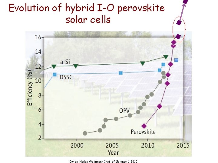
Evolution of hybrid I-O perovskite solar cells Cahen-Hodes Weizmann Inst. of Science 1 -2015

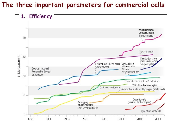
The three important parameters for commercial cells 1. Efficiency Cahen-Hodes Weizmann Inst. of Science 1 -2015

Shockley-Queisser* (SQ) Limit Cahen-Hodes Weizmann Inst. of Science 1 -2015

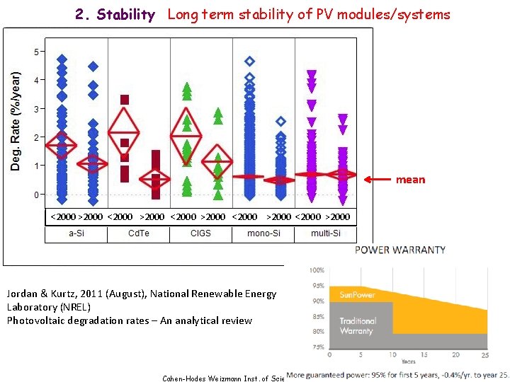
2. Stability Long term stability of PV modules/systems mean <2000 >2000 <2000 >2000 Jordan & Kurtz, 2011 (August), National Renewable Energy Laboratory (NREL) Photovoltaic degradation rates – An analytical review Cahen-Hodes Weizmann Inst. of Science 1 -2015

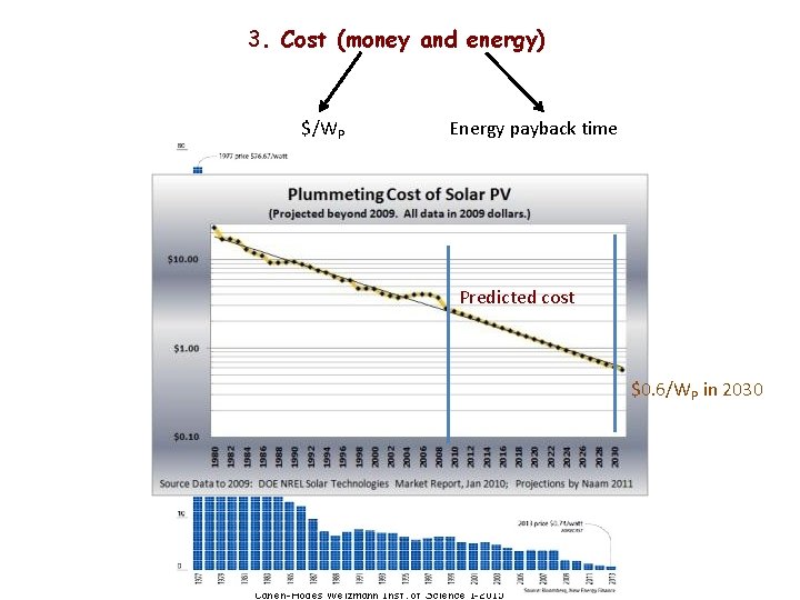
3. Cost (money and energy) $/WP Energy payback time Predicted cost $0. 6/WP in 2030 Cahen-Hodes Weizmann Inst. of Science 1 -2015

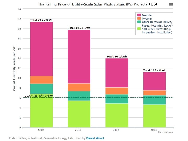
(US) Cahen-Hodes Weizmann Inst. of Science 1 -2015

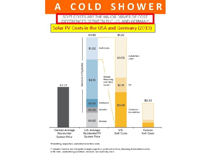
A COLD SHOWER Solar PV Costs in the USA and Germany (2013) Cahen-Hodes Weizmann Inst. of Science 1 -2015

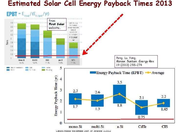
Estimated Solar Cell Energy Payback Times 2013 from First Solar website… Peng, Lu, Yang, Renew. Sustain. Energy Rev. 19 (2013) 255– 274 Cahen-Hodes Weizmann Inst. of Science 1 -2015

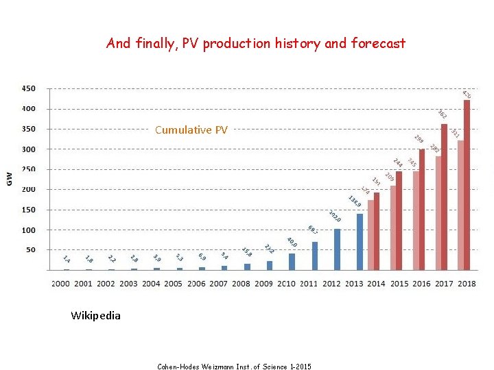
And finally, PV production history and forecast Cumulative PV Wikipedia Cahen-Hodes Weizmann Inst. of Science 1 -2015

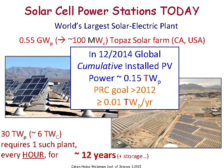
Solar Cell Power Stations TODAY World’s Largest Solar-Electric Plant 0. 55 GWp ( ~100 MWc) Topaz Solar farm (CA, USA) In 12/2014 Global Cumulative Installed PV Power ~ 0. 15 TWp PRC goal >2012 ≥ 0. 01 TWp/yr 30 TWp (~ 6 TWC) requires 1 such plant, every HOUR, for ~ 12 years (+ storage…) Cahen-Hodes Weizmann Inst. of Science 1 -2015