Electronics Diodes Introduction The simplest and most fundamental
- Slides: 66

Electronics - Diodes Introduction § § § The simplest and most fundamental nonlinear circuit element is the diode. It is a two terminal device like a resistor but the two terminals are not interchangeable. We will start by describing an “ideal” diode and then look at how closely a real diode approximates the ideal situation. We will be considering silicon diodes throughout this book. As electrical engineers we can analyze diode circuits if we have equations which describe the terminal characteristics of the device, but we need to look further and understand physically how the diode works since the diode is also the basis of the BJT and MOSFET devices we will be studying later in this course. One of the most common uses of diode is in rectifier circuits (conversion of ac signals to dc) so we will spend some time on examples and then look at some other diode applications We also need to look at how diode model parameters can be extracted for use in simulation programs such as SPICE. The parameters can then be used to simulate some of the application circuit examples. © REP 12/3/2020 EGRE 224 Page 3. 1 -1

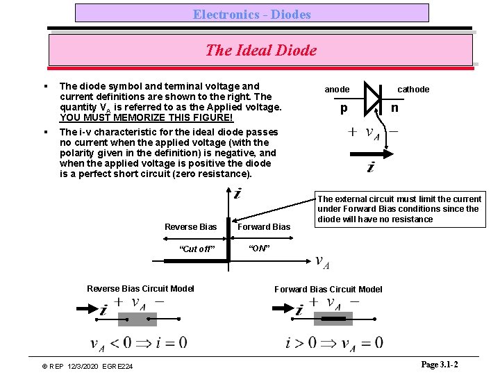
Electronics - Diodes The Ideal Diode § § The diode symbol and terminal voltage and current definitions are shown to the right. The quantity VA is referred to as the Applied voltage. YOU MUST MEMORIZE THIS FIGURE! The i-v characteristic for the ideal diode passes no current when the applied voltage (with the polarity given in the definition) is negative, and when the applied voltage is positive the diode is a perfect short circuit (zero resistance). Reverse Bias “Cut off” Reverse Bias Circuit Model © REP 12/3/2020 EGRE 224 Forward Bias anode p cathode n The external circuit must limit the current under Forward Bias conditions since the diode will have no resistance “ON” Forward Bias Circuit Model Page 3. 1 -2

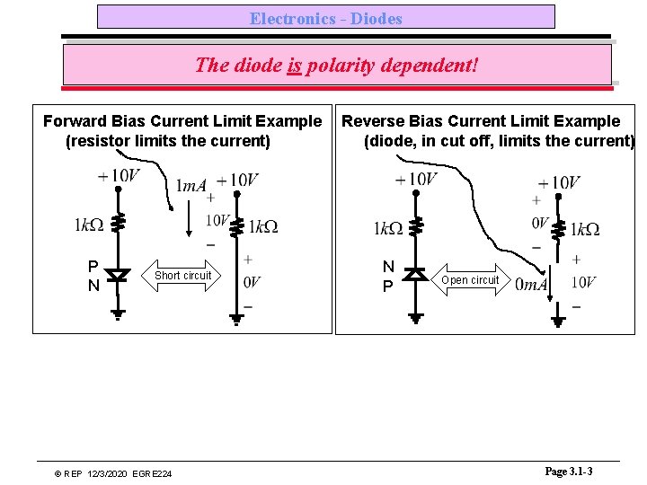
Electronics - Diodes The diode is polarity dependent! Forward Bias Current Limit Example (resistor limits the current) P N Short circuit © REP 12/3/2020 EGRE 224 Reverse Bias Current Limit Example (diode, in cut off, limits the current) N P Open circuit Page 3. 1 -3

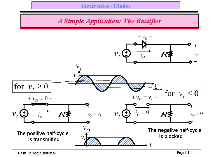
Electronics - Diodes A Simple Application: The Rectifier t The positive half-cycle is transmitted © REP 12/3/2020 EGRE 224 The negative half-cycle is blocked t Page 3. 1 -4

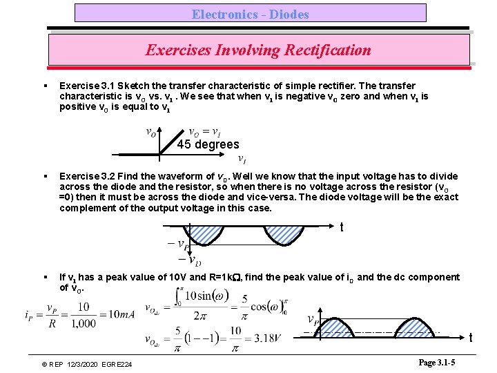
Electronics - Diodes Exercises Involving Rectification § Exercise 3. 1 Sketch the transfer characteristic of simple rectifier. The transfer characteristic is v. O vs. v. I. We see that when v. I is negative v. O zero and when v. I is positive v. O is equal to v. I 45 degrees § Exercise 3. 2 Find the waveform of v. D. Well we know that the input voltage has to divide across the diode and the resistor, so when there is no voltage across the resistor (v. O =0) then it must be across the diode and vice-versa. The diode voltage will be the exact complement of the output voltage in this case. t § If v. I has a peak value of 10 V and R=1 k. W, find the peak value of i. D and the dc component of v. O. t © REP 12/3/2020 EGRE 224 Page 3. 1 -5

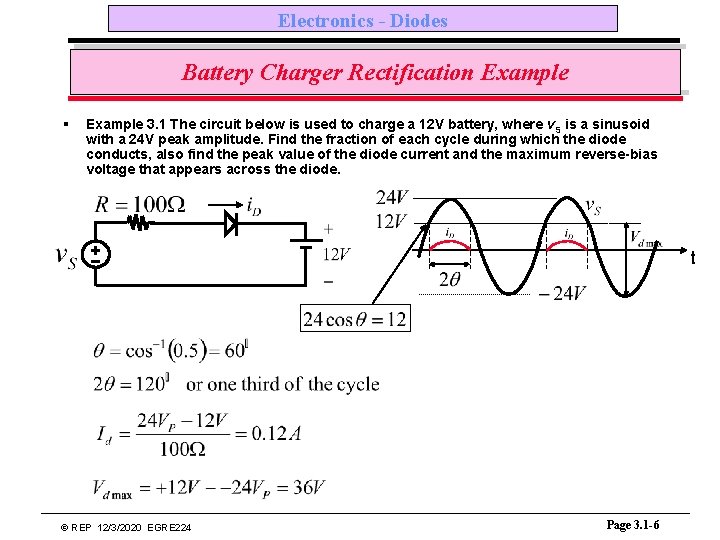
Electronics - Diodes Battery Charger Rectification Example § Example 3. 1 The circuit below is used to charge a 12 V battery, where v. S is a sinusoid with a 24 V peak amplitude. Find the fraction of each cycle during which the diode conducts, also find the peak value of the diode current and the maximum reverse-bias voltage that appears across the diode. t © REP 12/3/2020 EGRE 224 Page 3. 1 -6

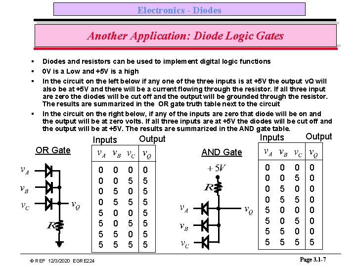
Electronics - Diodes Another Application: Diode Logic Gates § § Diodes and resistors can be used to implement digital logic functions 0 V is a Low and +5 V is a high In the circuit on the left below if any one of the three inputs is at +5 V the output v. Q will also be at +5 V and there will be a current flowing through the resistor. If all three input are zero the diodes will be cut off and the output will be grounded through the resistor. The results are summarized in the OR gate truth table next to the circuit In the circuit on the right below, if any of the inputs are zero that diode will be on and the output will be at zero volts. If all three inputs are at +5 V the diodes will be cut off and the output will be at +5 V. The results are summarized in the AND gate table. OR Gate AND Gate 0 0 5 5 © REP 12/3/2020 EGRE 224 Output Inputs 0 0 5 5 0 5 0 5 0 5 5 5 5 0 0 5 5 0 5 0 5 0 0 0 0 5 Page 3. 1 -7

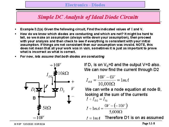
Electronics - Diodes Simple DC Analysis of Ideal Diode Circuits § § § Example 3. 2(a) Given the following circuit, Find the indicated values of I and V. How do we know which diodes are conducting and which are not? It might be hard to tell, so we make an assumption (always write down your assumption), then proceed with your analysis and then check to see if everything is consistent with your initial assumption. If things are not consistent then our assumption was invalid. NOTE, this does not mean that all your work was in vain, sometimes it is just as important to prove what is incorrect as what is correct. For now, lets assume that both diodes are conducting If D 1 is on VB=0 and the output V=0 also. We can now find the current through D 2 B We can write a node equation at node B, looking at the sum of the currents Therefore D 1 is on as assumed © REP 12/3/2020 EGRE 224 Page 3. 1 -8

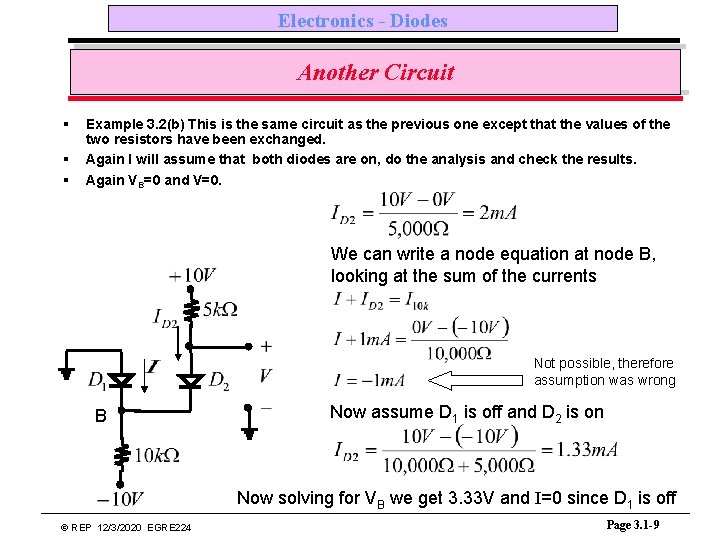
Electronics - Diodes Another Circuit § § § Example 3. 2(b) This is the same circuit as the previous one except that the values of the two resistors have been exchanged. Again I will assume that both diodes are on, do the analysis and check the results. Again VB=0 and V=0. We can write a node equation at node B, looking at the sum of the currents Not possible, therefore assumption was wrong B Now assume D 1 is off and D 2 is on Now solving for VB we get 3. 33 V and I=0 since D 1 is off © REP 12/3/2020 EGRE 224 Page 3. 1 -9

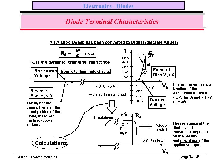
Electronics - Diodes Diode Terminal Characteristics An Analog sweep has been converted to Digital (discrete values) Rd = DV 1 = slope DI I 5 m. A Rd is the dynamic (changing) resistance Breakdown Voltage slope = 4 m. A DI 3 m. A from -6 to -hundreds of volts Reverse Bias Va < 0 The higher the doping levels of the n and p sides of the diode, the lower the breakdown voltage. Calculations DV 2 m. A 1 m. A slightly negative - 1 m. A - 2 m. A (+0. 2 volt increments) DI DV Forward Bias Va > 0 1. 0 Va - 3 m. A - 4 m. A Turn-on Voltage Rd breakdown “Off” R is high The resistance of the “closed” diode is not switch constant, it depends on the polarity “on” R is low and magnitude of the applied voltage Va © REP 12/3/2020 EGRE 224 The turn-on voltge is a function of the semiconductor used. ~ 0. 7 V for Si and ~ 1. 7 V for Ga. As Page 3. 1 -10

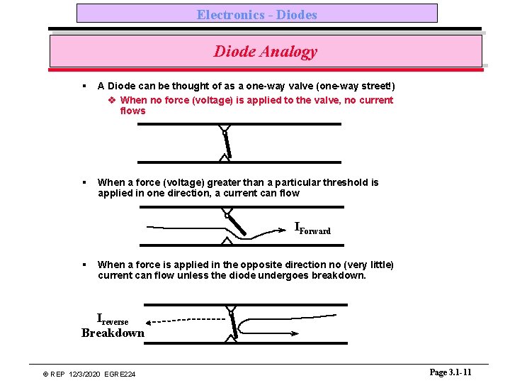
Electronics - Diodes Diode Analogy § A Diode can be thought of as a one-way valve (one-way street!) v When no force (voltage) is applied to the valve, no current flows § When a force (voltage) greater than a particular threshold is applied in one direction, a current can flow IForward § When a force is applied in the opposite direction no (very little) current can flow unless the diode undergoes breakdown. Ireverse Breakdown © REP 12/3/2020 EGRE 224 Page 3. 1 -11

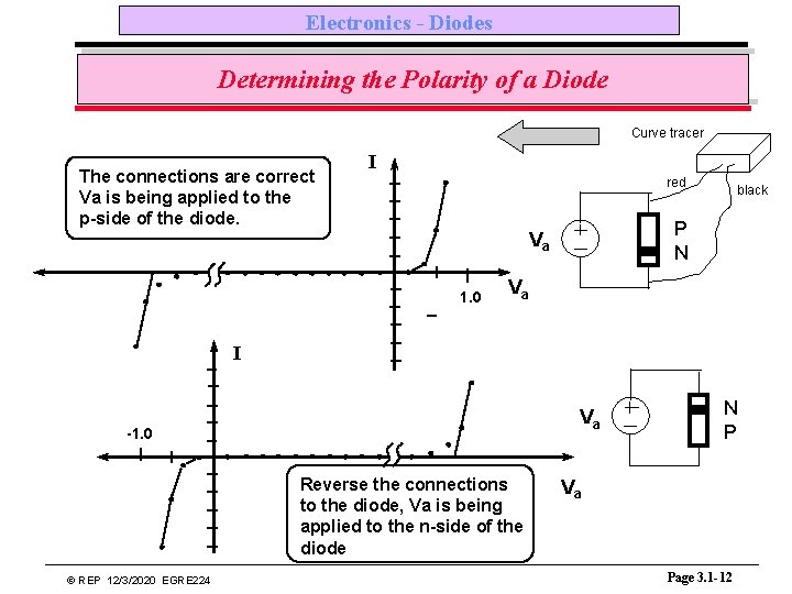
Electronics - Diodes Determining the Polarity of a Diode Curve tracer The connections are correct Va is being applied to the p-side of the diode. I red P N Va 1. 0 black Va I Va -1. 0 Reverse the connections to the diode, Va is being applied to the n-side of the diode © REP 12/3/2020 EGRE 224 N P Va Page 3. 1 -12

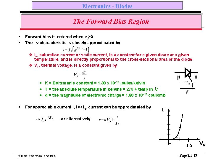
Electronics - Diodes The Forward Bias Region § § Forward-bias is entered when va>0 The i-v characteristic is closely approximated by v Is, saturation current or scale current, is a constant for a given diode at a given temperature, and is directly proportional to the cross-sectional area of the diode v VT, thermal voltage, is a constant given by n p w K = Boltzman’s constant = 1. 38 x 10 -23 joules/kelvin w T = the absolute temperature in kelvins = 273 + temp in C w q = the magnitude of electronic charge = 1. 60 x 10 -19 coulomb § For appreciable current i, i >>IS, current can be approximated by I or alternatively 1. 0 © REP 12/3/2020 EGRE 224 Page 3. 1 -13 Va

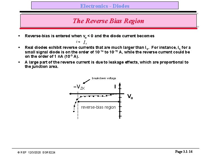
Electronics - Diodes The Reverse Bias Region § Reverse-bias is entered when va < 0 and the diode current becomes § Real diodes exhibit reverse currents that are much larger than IS. For instance, IS for a small signal diode is on the order of 10 -14 to 10 -15 A, while the reverse current could be on the order of 1 n. A (10 -9 A). A large part of the reverse current is due to leakage effects, which are proportional to the junction area. § breakdown voltage VZK I Va reverse-bias region © REP 12/3/2020 EGRE 224 Page 3. 1 -14

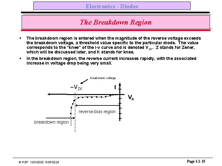
Electronics - Diodes The Breakdown Region § § The breakdown region is entered when the magnitude of the reverse voltage exceeds the breakdown voltage, a threshold value specific to the particular diode. The value corresponds to the “knee” of the i-v curve and is denoted VZK. Z stands for Zener, which will be discussed later, and K stands for knee. In the breakdown region, the reverse current increases rapidly, with the associated increase in voltage drop being very small. breakdown voltage VZK I Va reverse-bias region breakdown region © REP 12/3/2020 EGRE 224 Page 3. 1 -15

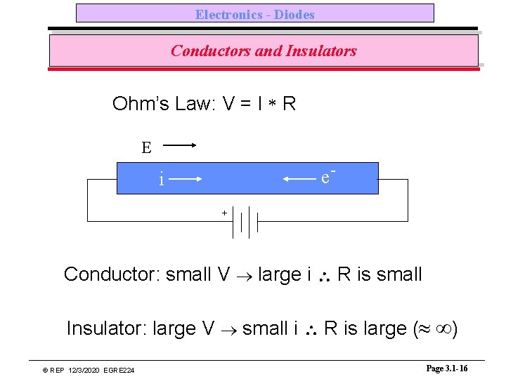
Electronics - Diodes Conductors and Insulators Ohm’s Law: V = I * R E e- i + Conductor: small V ® large i R is small Insulator: large V ® small i R is large (» ¥) © REP 12/3/2020 EGRE 224 Page 3. 1 -16

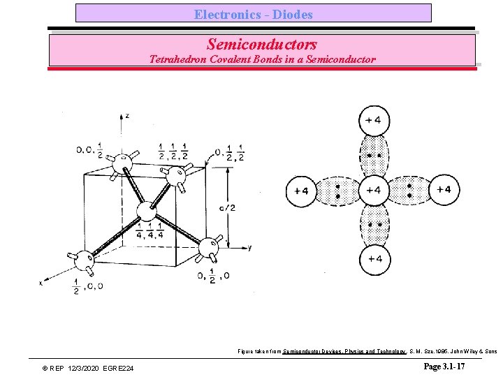
Electronics - Diodes Semiconductors Tetrahedron Covalent Bonds in a Semiconductor Figure taken from Semiconductor Devices, Physics and Technology , S. M. Sze, 1985, John Wiley & Sons © REP 12/3/2020 EGRE 224 Page 3. 1 -17

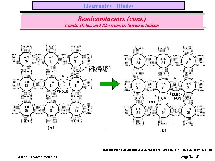
Electronics - Diodes Semiconductors (cont. ) Bonds, Holes, and Electrons in Intrinsic Silicon Figure taken from Semiconductor Devices, Physics and Technology , S. M. Sze, 1985, John Wiley & Sons © REP 12/3/2020 EGRE 224 Page 3. 1 -18

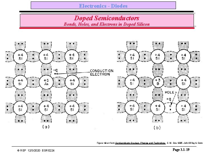
Electronics - Diodes Doped Semiconductors Bonds, Holes, and Electrons in Doped Silicon Figure taken from Semiconductor Devices, Physics and Technology , S. M. Sze, 1985, John Wiley & Sons © REP 12/3/2020 EGRE 224 Page 3. 1 -19

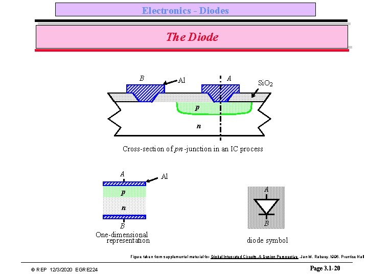
Electronics - Diodes The Diode B A Al Si. O 2 p n Cross-section of pn -junction in an IC process A Al A p n B One-dimensional representation B diode symbol Figure taken from supplemental material for Digital Integrated Circuits, A Design Perspective , Jan M. Rabaey, 1996, Prentice Hall © REP 12/3/2020 EGRE 224 Page 3. 1 -20

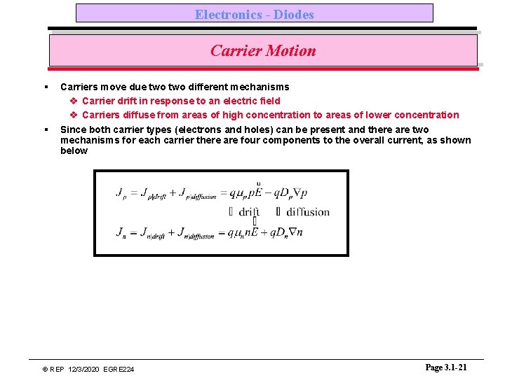
Electronics - Diodes Carrier Motion § § Carriers move due two different mechanisms v Carrier drift in response to an electric field v Carriers diffuse from areas of high concentration to areas of lower concentration Since both carrier types (electrons and holes) can be present and there are two mechanisms for each carrier there are four components to the overall current, as shown below © REP 12/3/2020 EGRE 224 Page 3. 1 -21

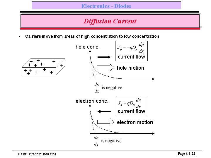
Electronics - Diodes Diffusion Current § Carriers move from areas of high concentration to low concentration hole conc. current flow ++ + + + ++ + hole motion electron conc. current flow electron motion © REP 12/3/2020 EGRE 224 Page 3. 1 -22

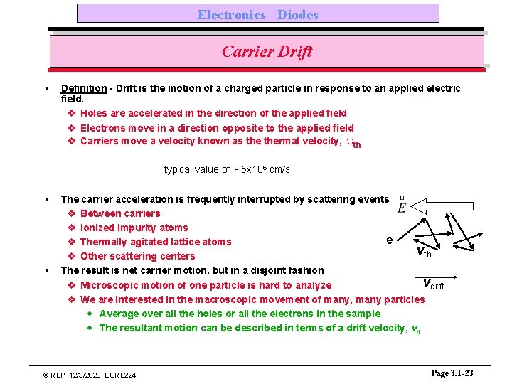
Electronics - Diodes Carrier Drift § Definition - Drift is the motion of a charged particle in response to an applied electric field. v Holes are accelerated in the direction of the applied field v Electrons move in a direction opposite to the applied field v Carriers move a velocity known as thermal velocity, uth typical value of ~ 5 x 106 cm/s § § The carrier acceleration is frequently interrupted by scattering events v Between carriers v Ionized impurity atoms ev Thermally agitated lattice atoms vth v Other scattering centers The result is net carrier motion, but in a disjoint fashion vdrift v Microscopic motion of one particle is hard to analyze v We are interested in the macroscopic movement of many, many particles w Average over all the holes or all the electrons in the sample w The resultant motion can be described in terms of a drift velocity, vd © REP 12/3/2020 EGRE 224 Page 3. 1 -23

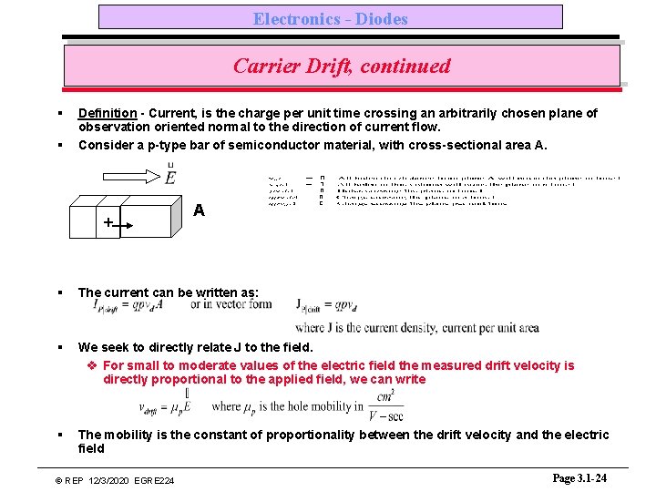
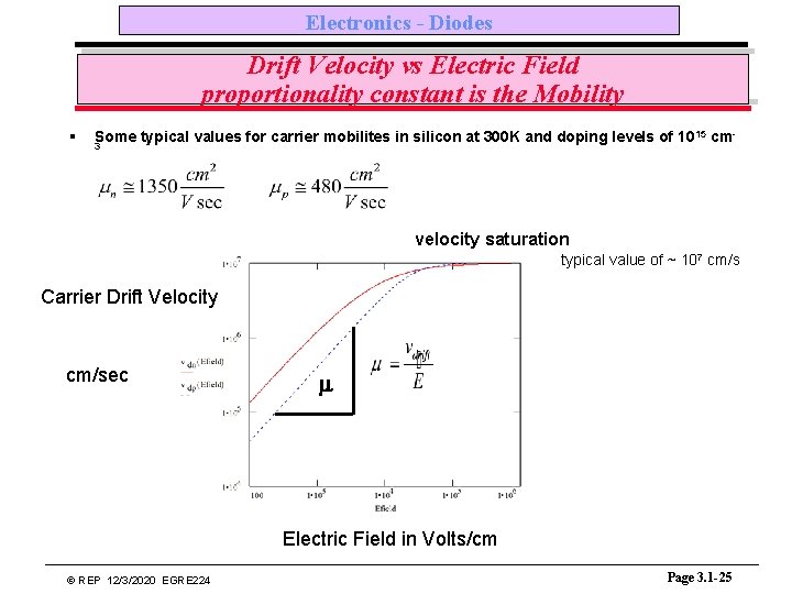
Electronics - Diodes Carrier Drift, continued § § Definition - Current, is the charge per unit time crossing an arbitrarily chosen plane of observation oriented normal to the direction of current flow. Consider a p-type bar of semiconductor material, with cross-sectional area A. + A § The current can be written as: § We seek to directly relate J to the field. v For small to moderate values of the electric field the measured drift velocity is directly proportional to the applied field, we can write § The mobility is the constant of proportionality between the drift velocity and the electric field © REP 12/3/2020 EGRE 224 Page 3. 1 -24

Electronics - Diodes Drift Velocity vs Electric Field proportionality constant is the Mobility § Some typical values for carrier mobilites in silicon at 300 K and doping levels of 1015 cm 3 velocity saturation typical value of ~ 107 cm/s Carrier Drift Velocity cm/sec m Electric Field in Volts/cm © REP 12/3/2020 EGRE 224 Page 3. 1 -25

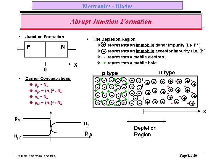
Electronics - Diodes Abrupt Junction Formation § Junction Formation N P 0 § § X The Depletion Region v + represents an immobile donor impurity (i. e. P+ ) v - represents an immobile acceptor impurity (i. e. B- ) v - represents a mobile electron v + represents a mobile hole p type - + - ++ -+ - +- + + ++ - - + -+ - Carrier Concentrations v pp ~ Na v np 0 ~ (ni )2 / Na v nn ~ Nd v pn 0 ~ (ni )2 / Nd - - - n type + + + - + -+ + ++ -+ + + - + -+ x pp np 0 © REP 12/3/2020 EGRE 224 nn pn 0 Depletion Region Page 3. 1 -26

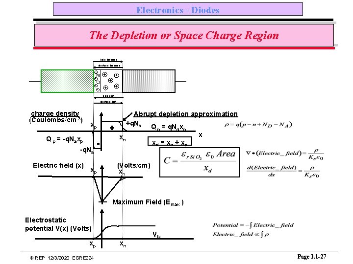
Electronics - Diodes The Depletion or Space Charge Region hole diffusion electron diffusion - + + + hole drift electron drift charge density (Coulombs/cm-3) xp Q p = -q. Naxp -q. Na Electric field (x) - xp + Abrupt depletion approximation +q. Nd Q n = q. Ndxn xd = x n + x p (Volts/cm) xn Maximum Field (Emax ) Electrostatic potential V(x) (Volts) xp © REP 12/3/2020 EGRE 224 Vbi xn Page 3. 1 -27

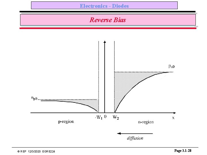
Electronics - Diodes Reverse Bias © REP 12/3/2020 EGRE 224 Page 3. 1 -28

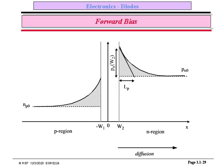
Electronics - Diodes Forward Bias © REP 12/3/2020 EGRE 224 Page 3. 1 -29

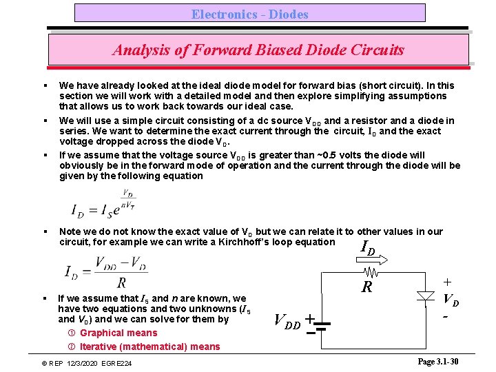
Electronics - Diodes Analysis of Forward Biased Diode Circuits § § § We have already looked at the ideal diode model forward bias (short circuit). In this section we will work with a detailed model and then explore simplifying assumptions that allows us to work back towards our ideal case. We will use a simple circuit consisting of a dc source V DD and a resistor and a diode in series. We want to determine the exact current through the circuit, ID and the exact voltage dropped across the diode VD. If we assume that the voltage source VDD is greater than ~0. 5 volts the diode will obviously be in the forward mode of operation and the current through the diode will be given by the following equation Note we do not know the exact value of VD but we can relate it to other values in our circuit, for example we can write a Kirchhoff’s loop equation ID If we assume that IS and n are known, we have two equations and two unknowns (IS and VD) and we can solve for them by Graphical means Iterative (mathematical) means © REP 12/3/2020 EGRE 224 R VDD + + VD - Page 3. 1 -30

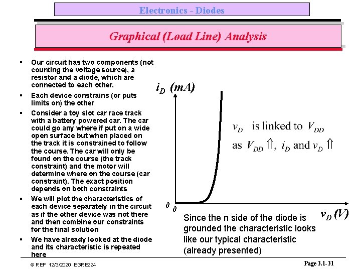
Electronics - Diodes Graphical (Load Line) Analysis § § § Our circuit has two components (not counting the voltage source), a resistor and a diode, which are connected to each other. D Each device constrains (or puts limits on) the other Consider a toy slot car race track with a battery powered car. The car could go any where if put on a wide open surface but when placed on the track it is constrained to follow the course. The car will only be found on the course (the track constraint) and the motor will determine where on the course (car constraint). The exact position depends on both constraints We will plot the characteristics of 0 each device separately in the circuit 0 as if the other device was not there and then combine our constraints for the final solution We have already looked at the diode and its characteristic is repeated here i (m. A) © REP 12/3/2020 EGRE 224 Since the n side of the diode is grounded the characteristic looks like our typical characteristic (already presented) v. D (V) Page 3. 1 -31

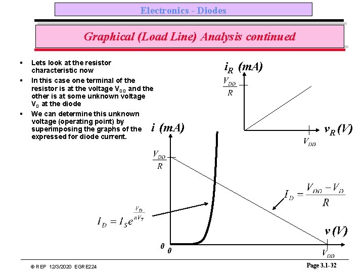
Electronics - Diodes Graphical (Load Line) Analysis continued § § § Lets look at the resistor characteristic now In this case one terminal of the resistor is at the voltage VDD and the other is at some unknown voltage VD at the diode We can determine this unknown voltage (operating point) by superimposing the graphs of the expressed for diode current. i. R (m. A) i (m. A) v. R (V) v (V) 0 © REP 12/3/2020 EGRE 224 0 Page 3. 1 -32

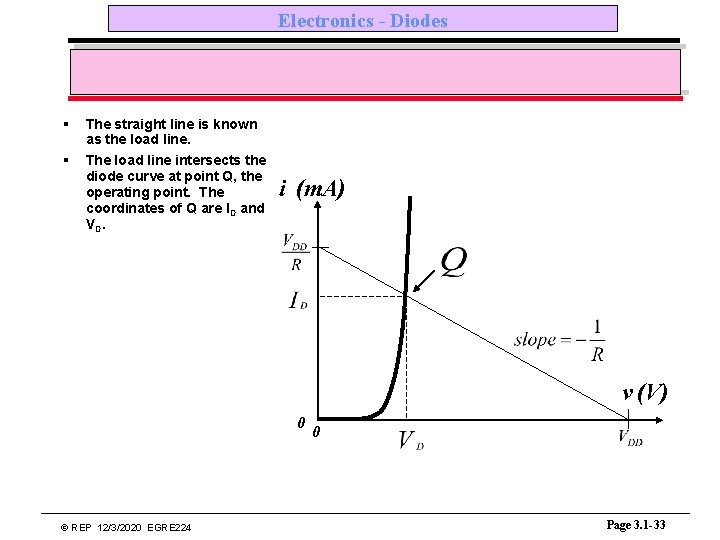
Electronics - Diodes § § The straight line is known as the load line. The load line intersects the diode curve at point Q, the operating point. The coordinates of Q are ID and VD. i (m. A) v (V) 0 © REP 12/3/2020 EGRE 224 0 Page 3. 1 -33

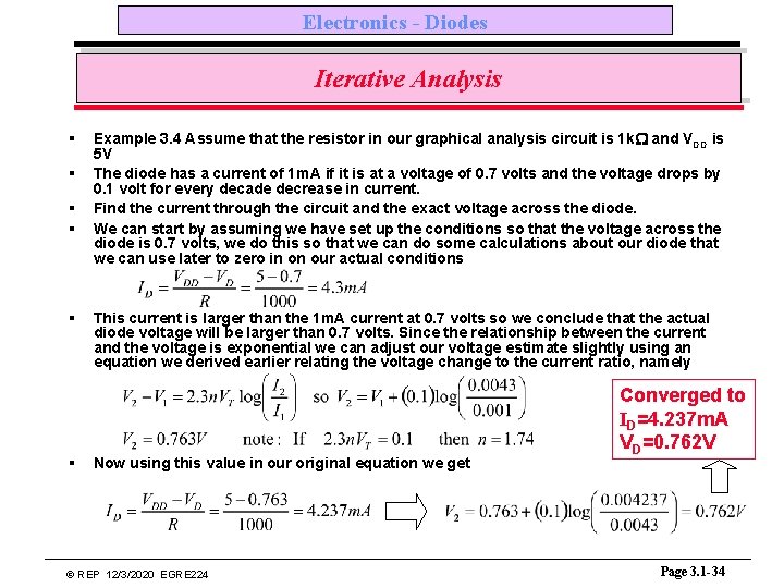
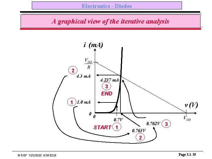
Electronics - Diodes Iterative Analysis § § § Example 3. 4 Assume that the resistor in our graphical analysis circuit is 1 k. W and VDD is 5 V The diode has a current of 1 m. A if it is at a voltage of 0. 7 volts and the voltage drops by 0. 1 volt for every decade decrease in current. Find the current through the circuit and the exact voltage across the diode. We can start by assuming we have set up the conditions so that the voltage across the diode is 0. 7 volts, we do this so that we can do some calculations about our diode that we can use later to zero in on our actual conditions This current is larger than the 1 m. A current at 0. 7 volts so we conclude that the actual diode voltage will be larger than 0. 7 volts. Since the relationship between the current and the voltage is exponential we can adjust our voltage estimate slightly using an equation we derived earlier relating the voltage change to the current ratio, namely Now using this value in our original equation we get © REP 12/3/2020 EGRE 224 Converged to ID=4. 237 m. A VD=0. 762 V Page 3. 1 -34

Electronics - Diodes A graphical view of the iterative analysis i (m. A) 2 4. 3 m. A 4. 237 m. A 3 END 1 1. 0 m. A 0 v (V) 0 0. 7 V START 1 0. 762 V 3 0. 763 V 2 © REP 12/3/2020 EGRE 224 Page 3. 1 -35

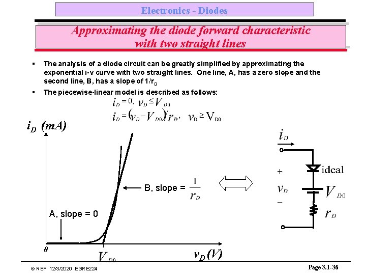
Electronics - Diodes Approximating the diode forward characteristic with two straight lines § The analysis of a diode circuit can be greatly simplified by approximating the exponential i-v curve with two straight lines. One line, A, has a zero slope and the second line, B, has a slope of 1/r. D § The piecewise-linear model is described as follows: i. D (m. A) B, slope = A, slope = 0 0 © REP 12/3/2020 EGRE 224 v. D (V) Page 3. 1 -36

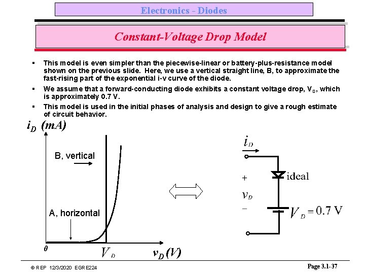
Electronics - Diodes Constant-Voltage Drop Model § § § This model is even simpler than the piecewise-linear or battery-plus-resistance model shown on the previous slide. Here, we use a vertical straight line, B, to approximate the fast-rising part of the exponential i-v curve of the diode. We assume that a forward-conducting diode exhibits a constant voltage drop, V D, which is approximately 0. 7 V. This model is used in the initial phases of analysis and design to give a rough estimate of circuit behavior. i. D (m. A) B, vertical A, horizontal 0 © REP 12/3/2020 EGRE 224 v. D (V) Page 3. 1 -37

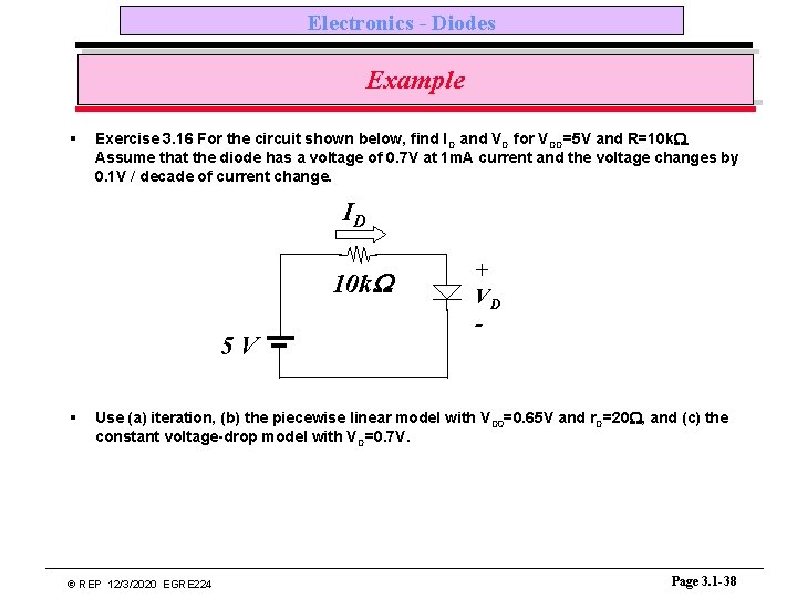
Electronics - Diodes Example § Exercise 3. 16 For the circuit shown below, find ID and VD for VDD=5 V and R=10 k. W. Assume that the diode has a voltage of 0. 7 V at 1 m. A current and the voltage changes by 0. 1 V / decade of current change. ID 10 k. W 5 V § + VD - Use (a) iteration, (b) the piecewise linear model with VD 0=0. 65 V and r. D=20 W, and (c) the constant voltage-drop model with VD=0. 7 V. © REP 12/3/2020 EGRE 224 Page 3. 1 -38

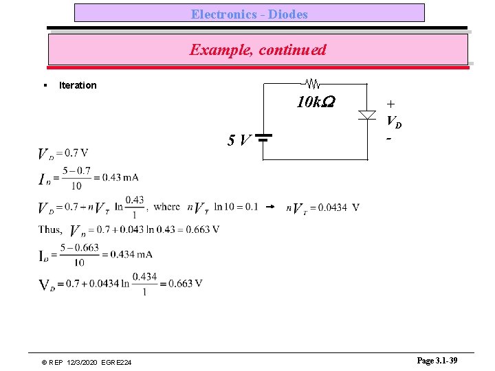
Electronics - Diodes Example, continued § Iteration 10 k. W 5 V © REP 12/3/2020 EGRE 224 + VD - Page 3. 1 -39

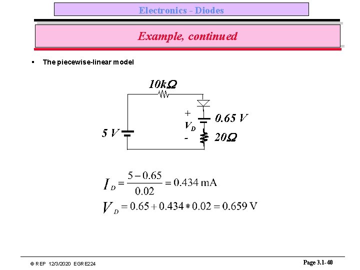
Electronics - Diodes Example, continued § The piecewise-linear model 10 k. W 5 V © REP 12/3/2020 EGRE 224 + VD - 0. 65 V 20 W Page 3. 1 -40

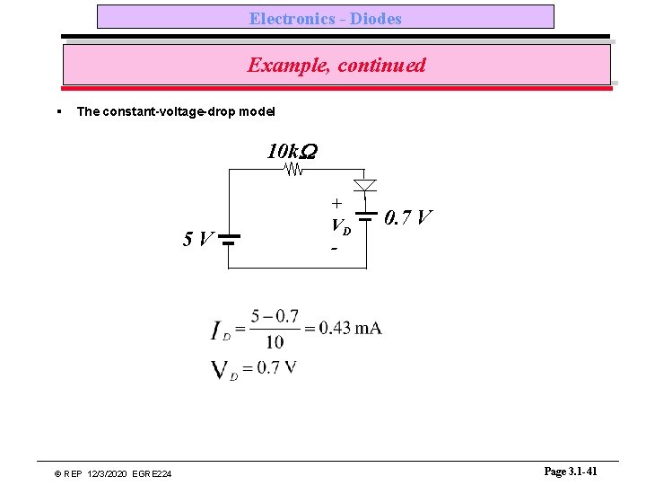
Electronics - Diodes Example, continued § The constant-voltage-drop model 10 k. W 5 V © REP 12/3/2020 EGRE 224 + VD - 0. 7 V Page 3. 1 -41

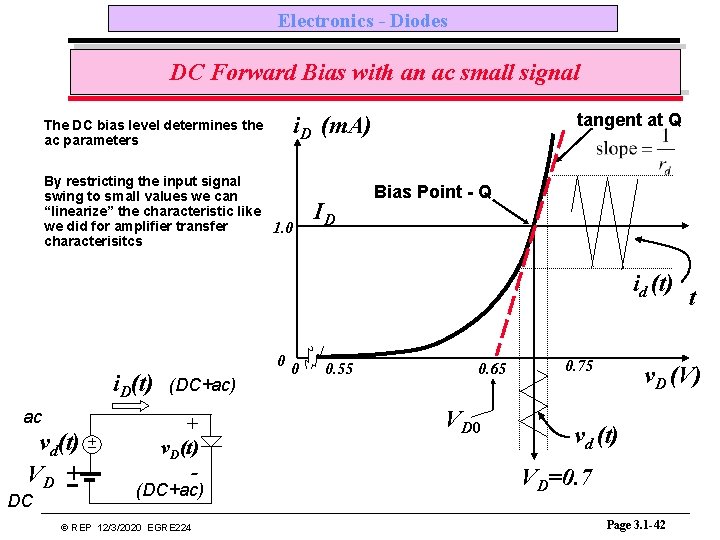
Electronics - Diodes DC Forward Bias with an ac small signal tangent at Q i. D (m. A) The DC bias level determines the ac parameters By restricting the input signal swing to small values we can “linearize” the characteristic like we did for amplifier transfer 1. 0 characterisitcs ID Bias Point - Q id (t) i. D(t) ac vd(t) VD + DC 0 (DC+ac) + v. D(t) - (DC+ac) © REP 12/3/2020 EGRE 224 0 0. 55 0. 65 VD 0 0. 75 t v. D (V) vd (t) VD=0. 7 Page 3. 1 -42

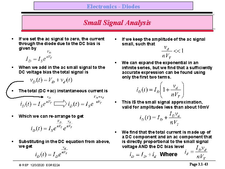
Electronics - Diodes Small Signal Analysis § If we set the ac signal to zero, the current through the diode due to the DC bias is given by § When we add in the ac small signal to the DC voltage bias the total signal is § The total (DC +ac) instantaneous current is § § § If we keep the amplitude of the ac signal small, such that § We can expand the exponential in an infinite series, but we find that a sufficiently accurate expression can be found using only the first two terms. § This IS the small signal approximation, valid for amplitudes less than about 10 m. V § We find that the total current is made up of a DC component and an ac component that is directly proportional to the small signal voltage AND the DC bias level Which we can re-arrange to get Substituting in the DC equation from above, we get Where © REP 12/3/2020 EGRE 224 Page 3. 1 -43

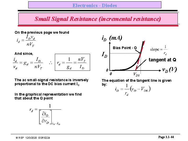
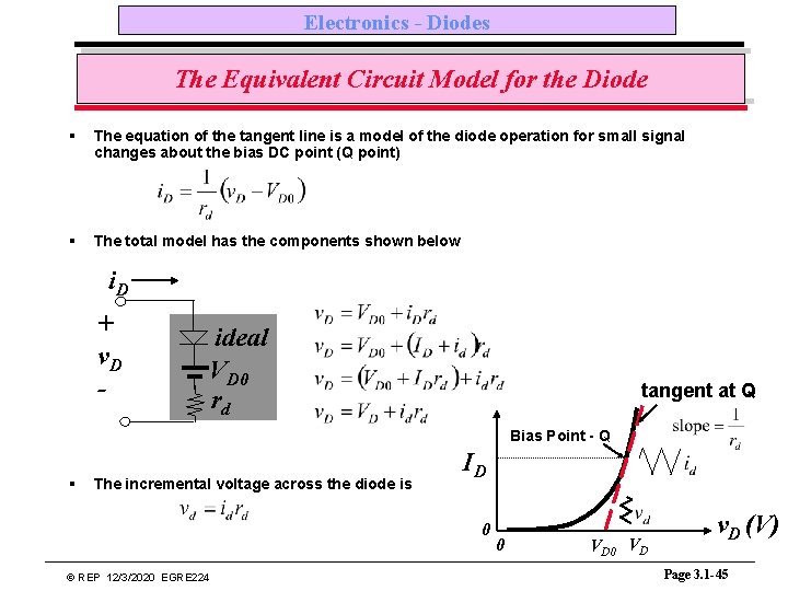
Electronics - Diodes Small Signal Resistance (incremental resistance) On the previous page we found i. D (m. A) Bias Point - Q And since, ID 0 The ac small-signal resistance is inversely proportional to the DC bias current ID tangent at Q 0 VD 0 v. D (V) The equation of the tangent line is given by: In the graphical representation we find that about the Q point © REP 12/3/2020 EGRE 224 Page 3. 1 -44

Electronics - Diodes The Equivalent Circuit Model for the Diode § The equation of the tangent line is a model of the diode operation for small signal changes about the bias DC point (Q point) § The total model has the components shown below i. D + v. D - ideal VD 0 rd tangent at Q Bias Point - Q § The incremental voltage across the diode is ID 0 © REP 12/3/2020 EGRE 224 0 VD v. D (V) Page 3. 1 -45

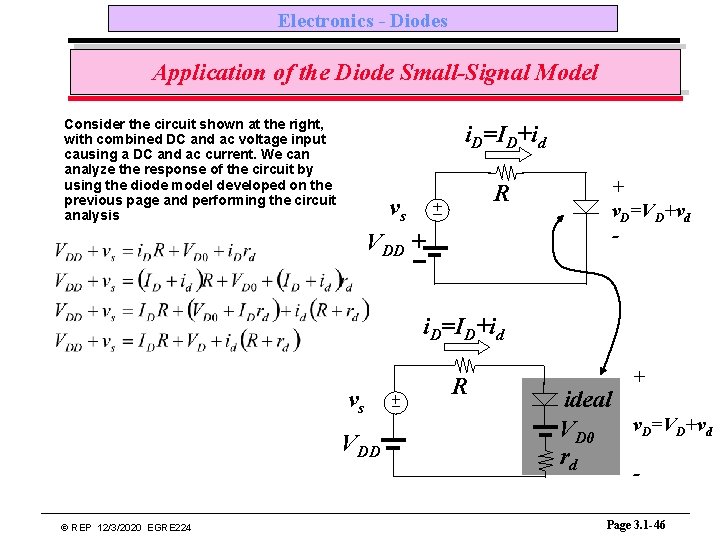
Electronics - Diodes Application of the Diode Small-Signal Model Consider the circuit shown at the right, with combined DC and ac voltage input causing a DC and ac current. We can analyze the response of the circuit by using the diode model developed on the previous page and performing the circuit analysis i. D=ID+id R vs VDD + + v. D=VD+vd - i. D=ID+id vs VDD R + ideal v. D=VD+vd VD 0 rd - © REP 12/3/2020 EGRE 224 Page 3. 1 -46

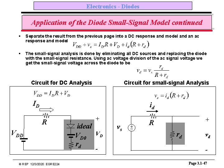
Electronics - Diodes Application of the Diode Small-Signal Model continued § Separate the result from the previous page into a DC response and model and an ac response and model § The small-signal analysis is done by eliminating all DC sources and replacing the diode with the small-signal resistance. Using ac voltage division of the ac signal voltage we get the small-signal voltage across the diode to be Circuit for DC Analysis Circuit for small-signal Analysis ID id R VDD + ideal VD 0 VD rd - © REP 12/3/2020 EGRE 224 vs + R rd vd Page 3. 1 -47

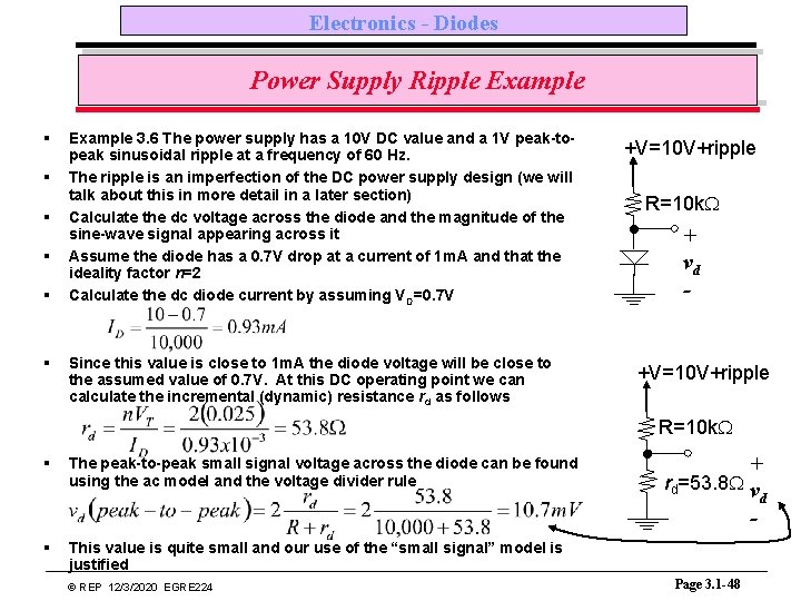
Electronics - Diodes Power Supply Ripple Example § § § Example 3. 6 The power supply has a 10 V DC value and a 1 V peak-topeak sinusoidal ripple at a frequency of 60 Hz. The ripple is an imperfection of the DC power supply design (we will talk about this in more detail in a later section) Calculate the dc voltage across the diode and the magnitude of the sine-wave signal appearing across it Assume the diode has a 0. 7 V drop at a current of 1 m. A and that the ideality factor n=2 Calculate the dc diode current by assuming VD=0. 7 V Since this value is close to 1 m. A the diode voltage will be close to the assumed value of 0. 7 V. At this DC operating point we can calculate the incremental (dynamic) resistance rd as follows +V=10 V+ripple R=10 k. W + vd - +V=10 V+ripple R=10 k. W § The peak-to-peak small signal voltage across the diode can be found using the ac model and the voltage divider rule § This value is quite small and our use of the “small signal” model is justified © REP 12/3/2020 EGRE 224 + rd=53. 8 W v d Page 3. 1 -48

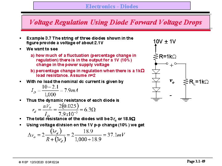
Electronics - Diodes Voltage Regulation Using Diode Forward Voltage Drops § § § Example 3. 7 The string of three diodes shown in the figure provide a voltage of about 2. 1 V We want to see a) how much of a fluctuation (percentage change in regulation) there is in the output for a 1 V (10%) change in the power supply voltage b) percentage change in regulation when there is a 1 k. W load resistance. Assume n=2 With no load the nominal dc current is given by § Thus the dynamic resistance of each diode is § § The total resistance of the diodes will be 3 rd or 18. 9 W Using voltage division on the 1 V p-p change (10%) we get © REP 12/3/2020 EGRE 224 10 V + 1 V R=1 k. W + vo RL=1 k. W - Page 3. 1 -49

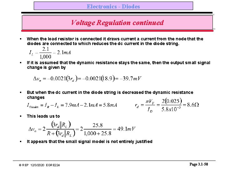
Electronics - Diodes Voltage Regulation continued § When the load resistor is connected it draws current a current from the node that the diodes are connected to which reduces the dc current in the diode string. § If it is assumed that the dynamic resistance stays the same, then the output small signal change is given by § But when the dc current in the diode string is decreased the dynamic resistance changes § This leads us to § It appears that the small signal model is not entirely justified © REP 12/3/2020 EGRE 224 Page 3. 1 -50

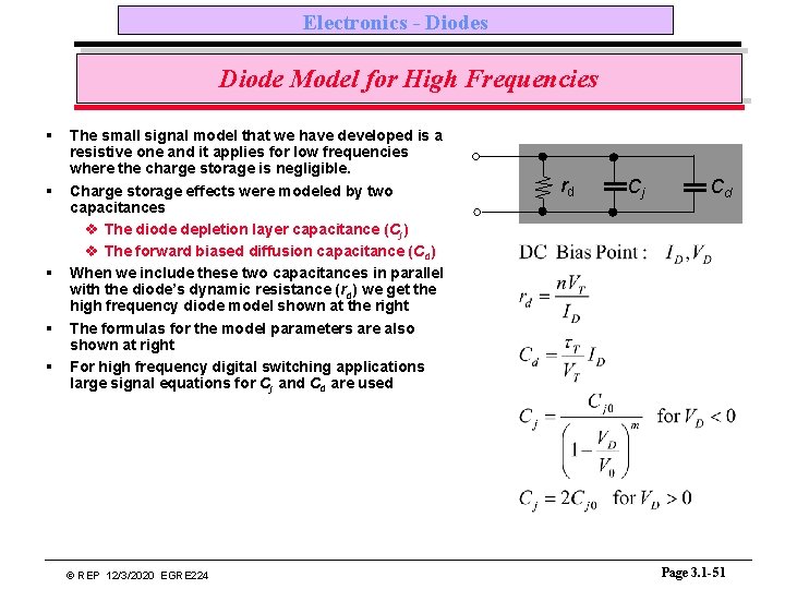
Electronics - Diodes Diode Model for High Frequencies § § § The small signal model that we have developed is a resistive one and it applies for low frequencies where the charge storage is negligible. Charge storage effects were modeled by two capacitances v The diode depletion layer capacitance (Cj) v The forward biased diffusion capacitance (Cd) When we include these two capacitances in parallel with the diode’s dynamic resistance (rd) we get the high frequency diode model shown at the right The formulas for the model parameters are also shown at right For high frequency digital switching applications large signal equations for Cj and Cd are used © REP 12/3/2020 EGRE 224 rd Cj Cd Page 3. 1 -51

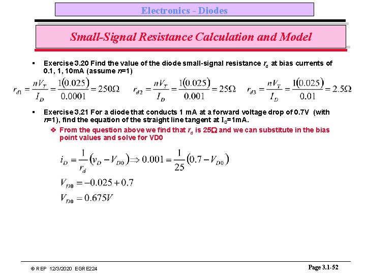
Electronics - Diodes Small-Signal Resistance Calculation and Model § Exercise 3. 20 Find the value of the diode small-signal resistance rd at bias currents of 0. 1, 1, 10 m. A (assume n=1) § Exercise 3. 21 For a diode that conducts 1 m. A at a forward voltage drop of 0. 7 V (with n=1), find the equation of the straight line tangent at ID=1 m. A. v From the question above we find that rd is 25 W and we can substitute in the bias point values and solve for VD 0 © REP 12/3/2020 EGRE 224 Page 3. 1 -52

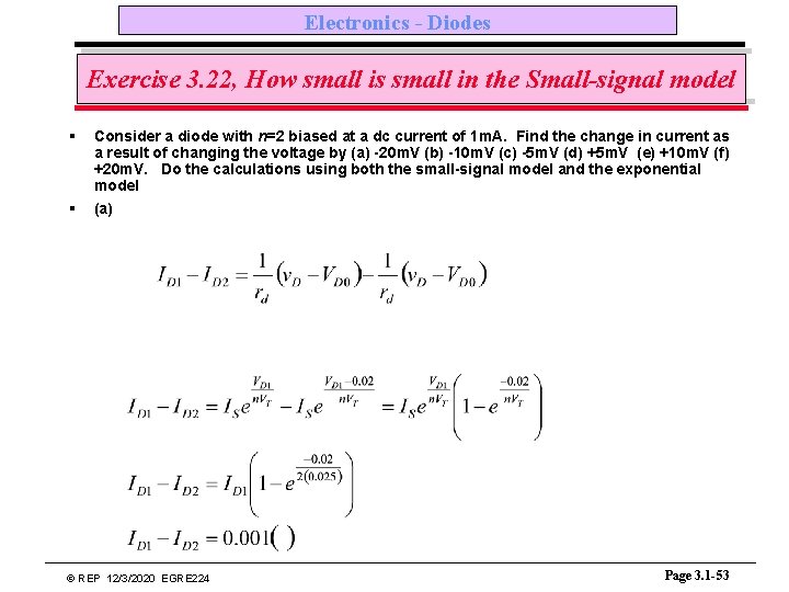
Electronics - Diodes Exercise 3. 22, How small is small in the Small-signal model § § Consider a diode with n=2 biased at a dc current of 1 m. A. Find the change in current as a result of changing the voltage by (a) -20 m. V (b) -10 m. V (c) -5 m. V (d) +5 m. V (e) +10 m. V (f) +20 m. V. Do the calculations using both the small-signal model and the exponential model (a) © REP 12/3/2020 EGRE 224 Page 3. 1 -53

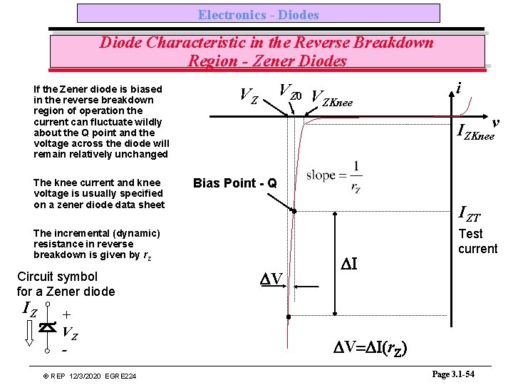
Electronics - Diodes Diode Characteristic in the Reverse Breakdown Region - Zener Diodes If the Zener diode is biased in the reverse breakdown region of operation the current can fluctuate wildly about the Q point and the voltage across the diode will remain relatively unchanged The knee current and knee voltage is usually specified on a zener diode data sheet VZ 0 V ZKnee VZ IZKneev Bias Point - Q IZT The incremental (dynamic) resistance in reverse breakdown is given by r. Z Circuit symbol for a Zener diode IZ + VZ © REP 12/3/2020 EGRE 224 i DV DI Test current DV=DI(r. Z) Page 3. 1 -54

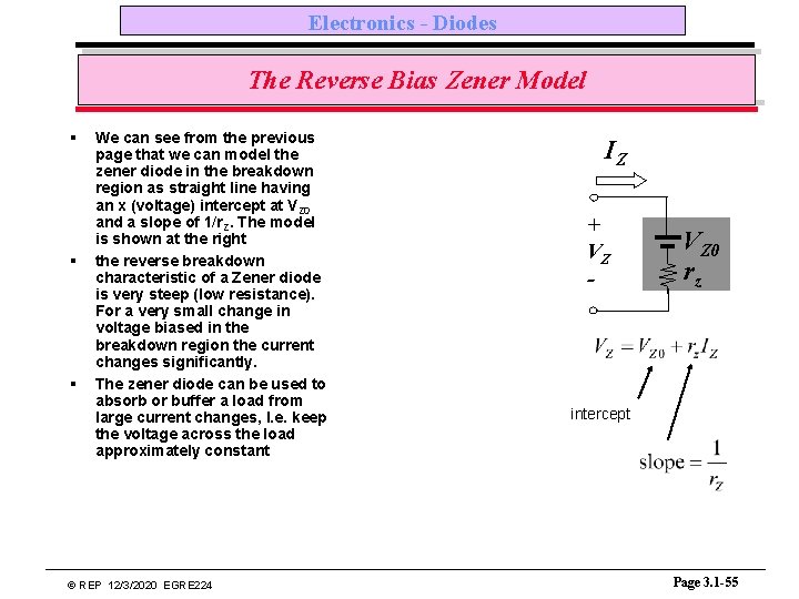
Electronics - Diodes The Reverse Bias Zener Model § § § We can see from the previous page that we can model the zener diode in the breakdown region as straight line having an x (voltage) intercept at VZ 0 and a slope of 1/r. Z. The model is shown at the right the reverse breakdown characteristic of a Zener diode is very steep (low resistance). For a very small change in voltage biased in the breakdown region the current changes significantly. The zener diode can be used to absorb or buffer a load from large current changes, I. e. keep the voltage across the load approximately constant © REP 12/3/2020 EGRE 224 IZ + VZ - VZ 0 rz intercept Page 3. 1 -55

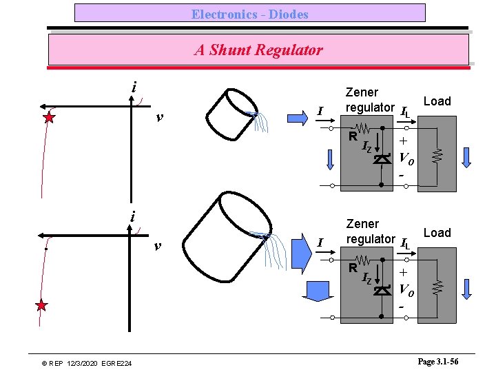
Electronics - Diodes A Shunt Regulator i v I Zener regulator I L R i v I + VO - Zener regulator I L R © REP 12/3/2020 EGRE 224 IZ IZ Load + VO - Page 3. 1 -56

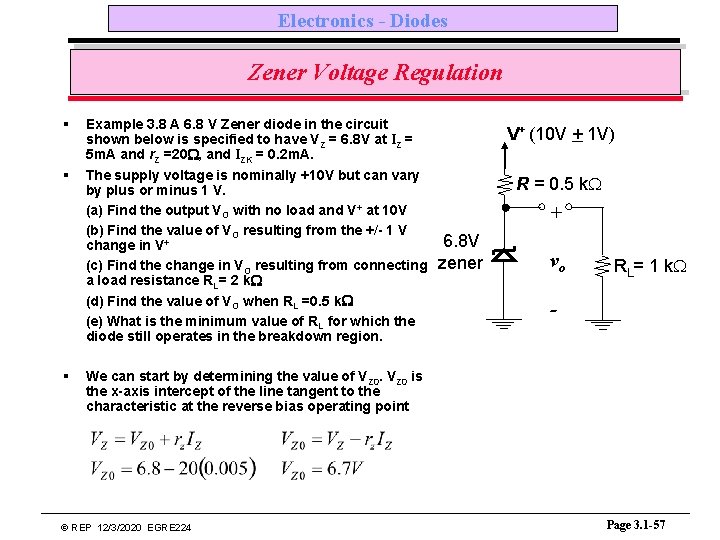
Electronics - Diodes Zener Voltage Regulation § § § Example 3. 8 A 6. 8 V Zener diode in the circuit shown below is specified to have VZ = 6. 8 V at IZ = 5 m. A and r. Z =20 W, and IZK = 0. 2 m. A. The supply voltage is nominally +10 V but can vary by plus or minus 1 V. (a) Find the output VO with no load and V+ at 10 V (b) Find the value of VO resulting from the +/- 1 V change in V+ (c) Find the change in VO resulting from connecting a load resistance RL= 2 k. W (d) Find the value of VO when RL =0. 5 k. W (e) What is the minimum value of RL for which the diode still operates in the breakdown region. V+ (10 V + 1 V) R = 0. 5 k. W + 6. 8 V zener vo RL= 1 k. W - We can start by determining the value of VZ 0 is the x-axis intercept of the line tangent to the characteristic at the reverse bias operating point © REP 12/3/2020 EGRE 224 Page 3. 1 -57

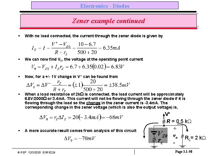
Electronics - Diodes Zener example continued § With no load connected, the current through the zener diode is given by § We can now find V 0, the voltage at the operating point current § Now, for a +/- 1 V change in V+ can be found from § When a load resistance of 2 k. W is connected, the load current will be approximately 6. 8 V/2000 W or 3. 4 m. A. This current will not be flowing through the zener diode if it is flowing through the load so the change in the zener current is -3. 4 m. A. The corresponding change in the zener voltage (which is also the output voltage) is, V+ R = 0. 5 k. W § A more accurate result comes from analysis of this circuit © REP 12/3/2020 EGRE 224 VZ 0 rz + vo - RL= 2 k. W Page 3. 1 -58

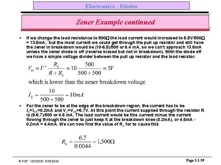
Electronics - Diodes Zener Example continued § If we change the load resistance to 500 W the load current would increased to 6. 8 V/500 W = 13. 6 m. A, but the most current we could get through the pull up resistor and still have the zener in breakdown would be (10 -6. 8)/500 or 6. 4 m. A, so we can’t approach 13. 6 m. A unless the zener diode is off (reverse biased but not in breakdown). With the diode off we have a simple voltage divider between the pull up resistor and the load resistor. § For the zener to be at the edge of the breakdown region, the current has to be IZ=IZK=0. 2 m. A and VZ=VZK=6. 7 V. At this point the current supplied through the resistor R is (9 -6. 7)/500 or 4. 6 m. A. The load current would be this current minus the current flowing through the zener to just keep it at the breakdown knee (0. 2 m. A), or 4. 6 m. A 0. 2 m. A = 4. 4 m. A. We can now find the value of RL for to cause this © REP 12/3/2020 EGRE 224 Page 3. 1 -59

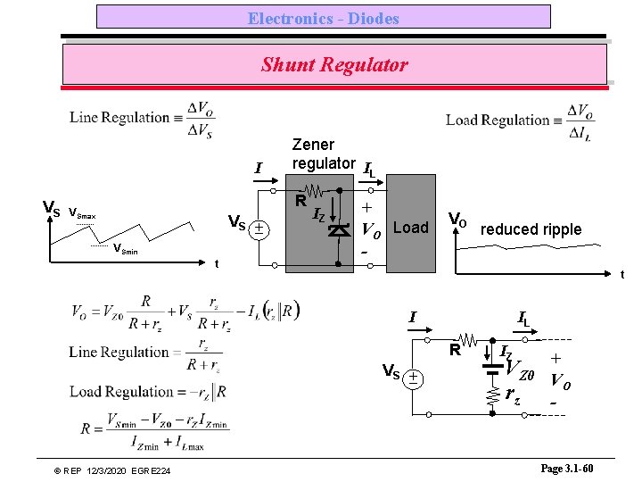
Electronics - Diodes Shunt Regulator I VS Zener regulator I L R VSmax VS VSmin t IZ + VO Load - VO reduced ripple t IL I R VS © REP 12/3/2020 EGRE 224 IZ + VZ 0 V rz - O Page 3. 1 -60

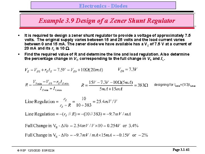
Electronics - Diodes Example 3. 9 Design of a Zener Shunt Regulator § § It is required to design a zener shunt regulator to provide a voltage of approximately 7. 5 volts. The original supply varies between 15 and 25 volts and the load current varies between 0 and 15 m. A. The zener diode we have available has a VZ of 7. 5 V at a current of 20 m. A and its r. Z is 10 W. Find the required value of R and determine the line and load regulation. Also determine the percentage change in VO corresponding to the full change in VS and IL. designing for Izmin=(1/3)ILmax © REP 12/3/2020 EGRE 224 Page 3. 1 -61

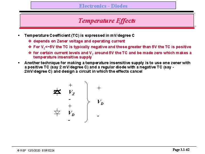
Electronics - Diodes Temperature Effects § § Temperature Coefficient (TC) is expressed in m. V/degree C v depends on Zener voltage and operating current v For VZ<~5 V the TC is typically negative and those greater than 5 V the TC is positive v for certain current levels and VZ around 5 V the TC and be made zero which makes a temperature insensitive supply Another technique for making a temperature insensitive supply is to use one zener with a positive TC (say 2 m. V/degree C) and a regular diode with a negative TC (say 2 m. V/degree C) and design a circuit in which the effects cancel + VZ + VD - © REP 12/3/2020 EGRE 224 + VD - Page 3. 1 -62

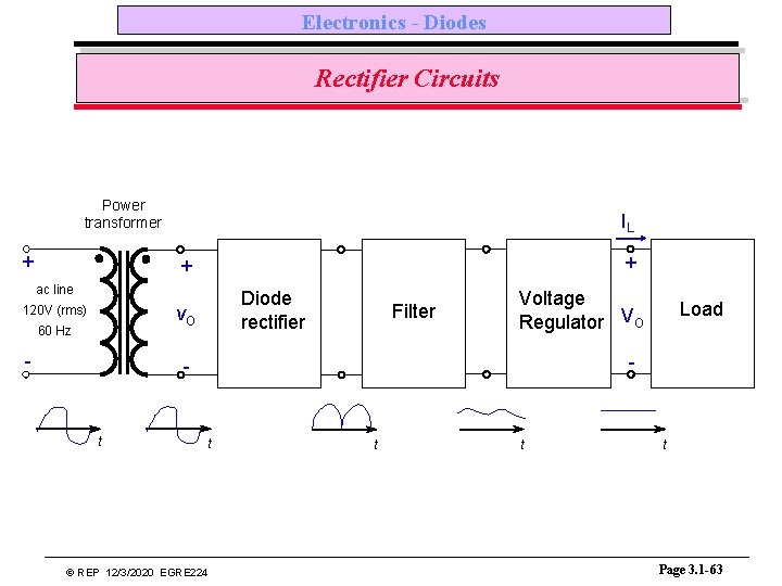
Electronics - Diodes Rectifier Circuits Power transformer + IL + + ac line Diode rectifier v. O 120 V (rms) 60 Hz - Filter Voltage Regulator VO - - t Load t © REP 12/3/2020 EGRE 224 t t t Page 3. 1 -63

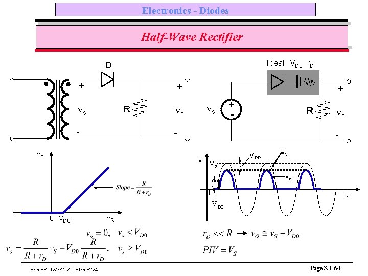
Electronics - Diodes Half-Wave Rectifier Ideal VD 0 r. D D + + vs R - + vs vo + - R - vo vo - v VS VD 0 v. S vo t VD 0 0 VD 0 © REP 12/3/2020 EGRE 224 v. S Page 3. 1 -64

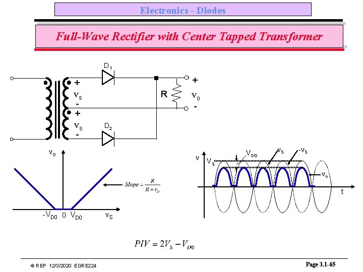
Electronics - Diodes Full-Wave Rectifier with Center Tapped Transformer D 1 + + vs R + vs - vo - D 2 vo v VS VD 0 v. S -v. S vo t -VD 0 0 VD 0 © REP 12/3/2020 EGRE 224 v. S Page 3. 1 -65

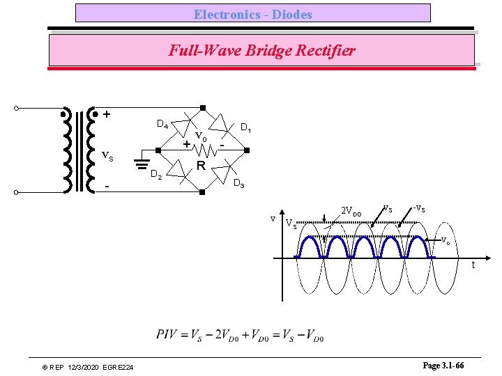
Electronics - Diodes Full-Wave Bridge Rectifier + D 4 + vs - D 2 vo D 1 - R D 3 v VS 2 VD 0 v. S -v. S vo t © REP 12/3/2020 EGRE 224 Page 3. 1 -66