ECE 243 Storage 1 Storage A storage mechanism
![Locality Example for (I=0; I<n; I++){ sum+=A[I]); } • What kinds of locality are Locality Example for (I=0; I<n; I++){ sum+=A[I]); } • What kinds of locality are](https://slidetodoc.com/presentation_image_h/246b8aa72932650634d47fd72bf3e1bf/image-9.jpg)
![Ex: ACCESS PATTERNS • Assume: – – 1 KB direct-mapped 32 B blocks A[i] Ex: ACCESS PATTERNS • Assume: – – 1 KB direct-mapped 32 B blocks A[i]](https://slidetodoc.com/presentation_image_h/246b8aa72932650634d47fd72bf3e1bf/image-39.jpg)

- Slides: 99

ECE 243 Storage 1

Storage • A storage mechanism can be two of: – fast – large – cheap • ie. , any given storage mechanism is either: – slow, small, or expensive • Examples: – fast/small/cheap: – slow/large/cheap: – fast/large/expensive: 2

Storage Topics • • Cache Design Memory Design Virtual Memory Disks 3

ECE 243 Caches 4

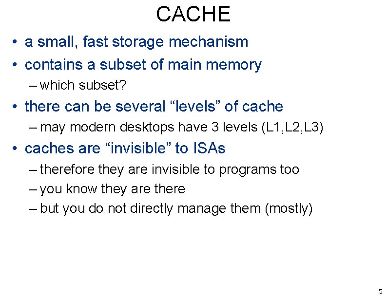
CACHE • a small, fast storage mechanism • contains a subset of main memory – which subset? • there can be several “levels” of cache – may modern desktops have 3 levels (L 1, L 2, L 3) • caches are “invisible” to ISAs – therefore they are invisible to programs too – you know they are there – but you do not directly manage them (mostly) 5

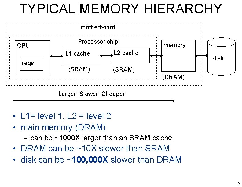
TYPICAL MEMORY HIERARCHY motherboard CPU Processor chip L 1 cache regs (SRAM) memory L 2 cache disk (SRAM) (DRAM) Larger, Slower, Cheaper • L 1= level 1, L 2 = level 2 • main memory (DRAM) – can be ~1000 X larger than an SRAM cache • DRAM can be ~10 X slower than SRAM • disk can be ~100, 000 X slower than DRAM 6

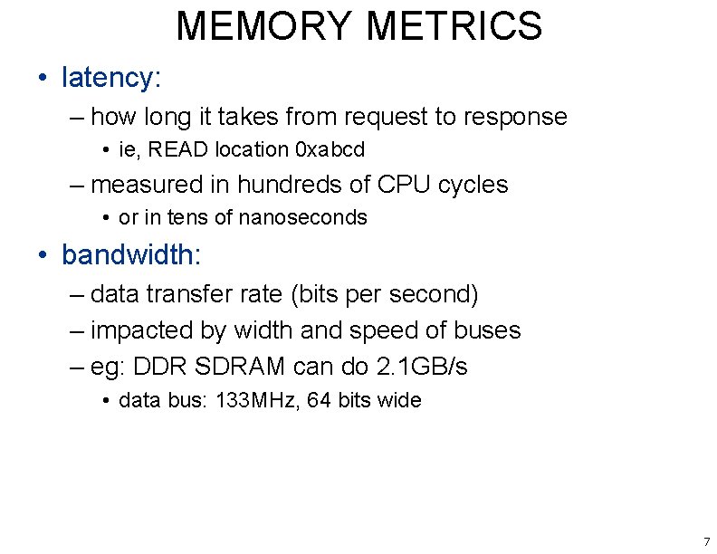
MEMORY METRICS • latency: – how long it takes from request to response • ie, READ location 0 xabcd – measured in hundreds of CPU cycles • or in tens of nanoseconds • bandwidth: – data transfer rate (bits per second) – impacted by width and speed of buses – eg: DDR SDRAM can do 2. 1 GB/s • data bus: 133 MHz, 64 bits wide 7

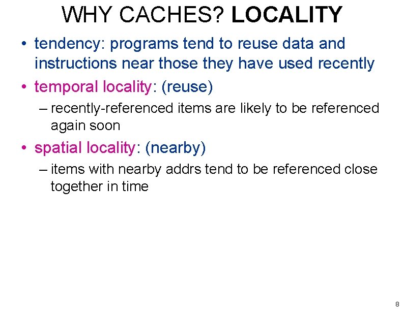
WHY CACHES? LOCALITY • tendency: programs tend to reuse data and instructions near those they have used recently • temporal locality: (reuse) – recently-referenced items are likely to be referenced again soon • spatial locality: (nearby) – items with nearby addrs tend to be referenced close together in time 8
![Locality Example for I0 In I sumAI What kinds of locality are Locality Example for (I=0; I<n; I++){ sum+=A[I]); } • What kinds of locality are](https://slidetodoc.com/presentation_image_h/246b8aa72932650634d47fd72bf3e1bf/image-9.jpg)
Locality Example for (I=0; I<n; I++){ sum+=A[I]); } • What kinds of locality are in this code? 9

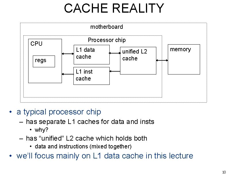
CACHE REALITY motherboard CPU regs Processor chip L 1 data cache unified L 2 cache memory L 1 inst cache • a typical processor chip – has separate L 1 caches for data and insts • why? – has “unified” L 2 cache which holds both • data and instructions (mixed together) • we’ll focus mainly on L 1 data cache in this lecture 10

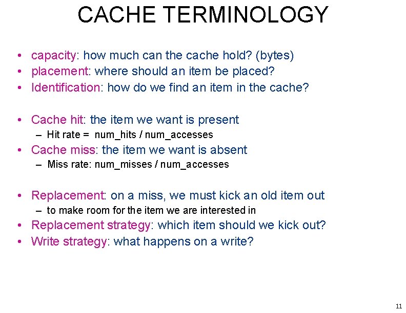
CACHE TERMINOLOGY • capacity: how much can the cache hold? (bytes) • placement: where should an item be placed? • Identification: how do we find an item in the cache? • Cache hit: the item we want is present – Hit rate = num_hits / num_accesses • Cache miss: the item we want is absent – Miss rate: num_misses / num_accesses • Replacement: on a miss, we must kick an old item out – to make room for the item we are interested in • Replacement strategy: which item should we kick out? • Write strategy: what happens on a write? 11

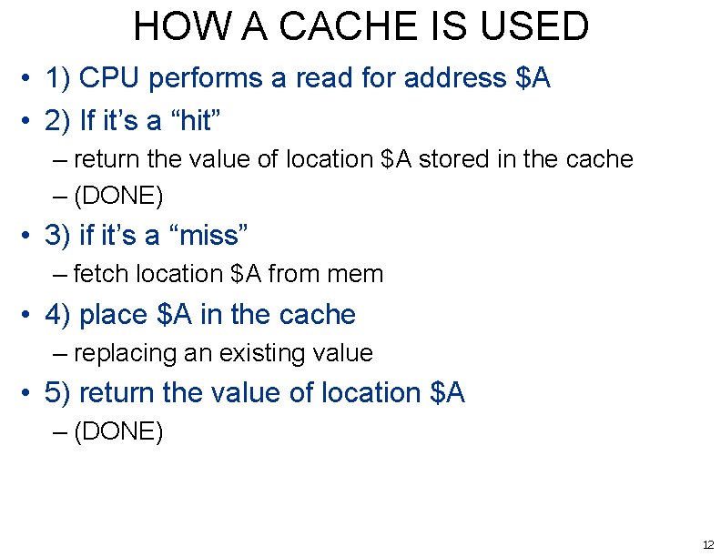
HOW A CACHE IS USED • 1) CPU performs a read for address $A • 2) If it’s a “hit” – return the value of location $A stored in the cache – (DONE) • 3) if it’s a “miss” – fetch location $A from mem • 4) place $A in the cache – replacing an existing value • 5) return the value of location $A – (DONE) 12

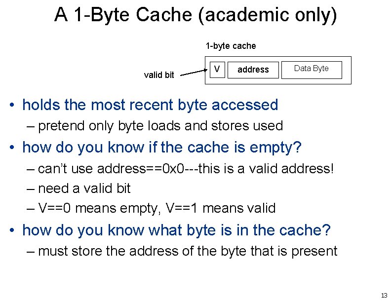
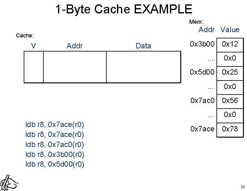
A 1 -Byte Cache (academic only) 1 -byte cache valid bit V address Data Byte • holds the most recent byte accessed – pretend only byte loads and stores used • how do you know if the cache is empty? – can’t use address==0 x 0 ---this is a valid address! – need a valid bit – V==0 means empty, V==1 means valid • how do you know what byte is in the cache? – must store the address of the byte that is present 13

1 -Byte Cache EXAMPLE Mem: Addr Value Cache: V Addr Data 0 x 3 b 00 0 x 12 … 0 x 0 0 x 5 d 00 0 x 25 … 0 x 0 0 x 7 ac 0 0 x 56 … ldb r 8, 0 x 7 ace(r 0) ldb r 8, 0 x 7 ac 0(r 0) ldb r 8, 0 x 3 b 00(r 0) ldb r 8, 0 x 5 d 00(r 0) 0 x 0 0 x 7 ace 0 x 78 14

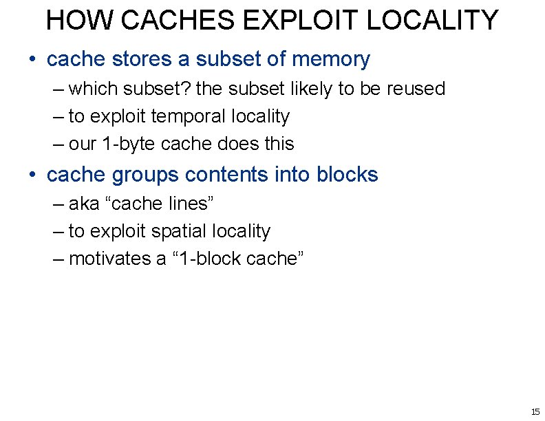
HOW CACHES EXPLOIT LOCALITY • cache stores a subset of memory – which subset? the subset likely to be reused – to exploit temporal locality – our 1 -byte cache does this • cache groups contents into blocks – aka “cache lines” – to exploit spatial locality – motivates a “ 1 -block cache” 15

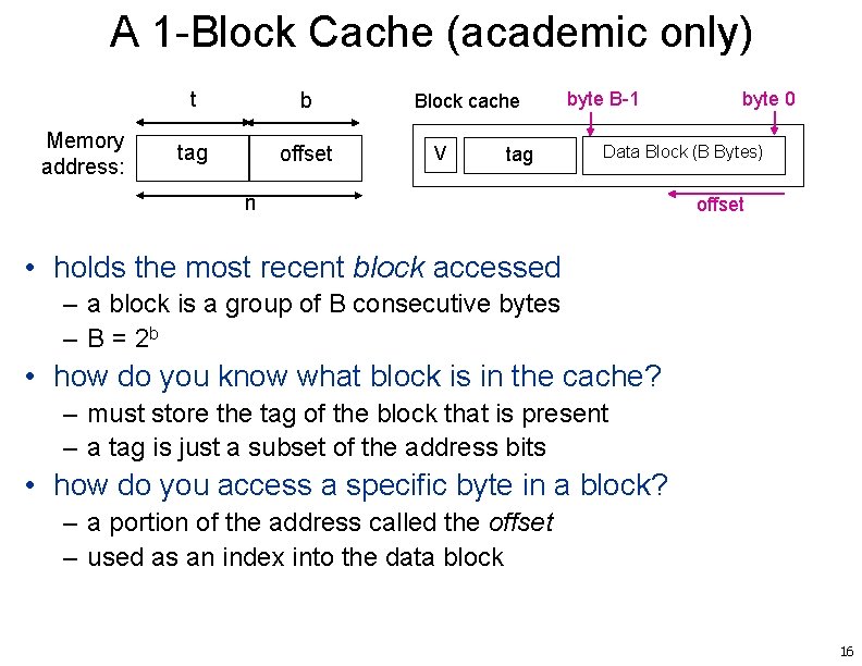
A 1 -Block Cache (academic only) Memory address: t b tag offset Block cache V tag byte B-1 byte 0 Data Block (B Bytes) n offset • holds the most recent block accessed – a block is a group of B consecutive bytes – B = 2 b • how do you know what block is in the cache? – must store the tag of the block that is present – a tag is just a subset of the address bits • how do you access a specific byte in a block? – a portion of the address called the offset – used as an index into the data block 16

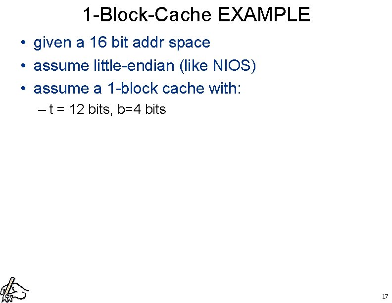
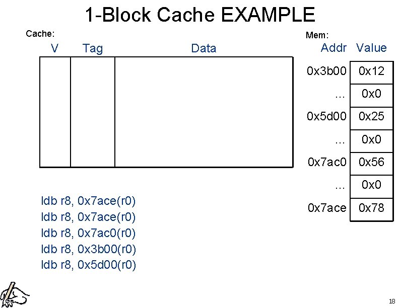
1 -Block-Cache EXAMPLE • given a 16 bit addr space • assume little-endian (like NIOS) • assume a 1 -block cache with: – t = 12 bits, b=4 bits 17

1 -Block Cache EXAMPLE Cache: V Mem: Tag Data Addr Value 0 x 3 b 00 0 x 12 … 0 x 0 0 x 5 d 00 0 x 25 … 0 x 0 0 x 7 ac 0 0 x 56 … ldb r 8, 0 x 7 ace(r 0) ldb r 8, 0 x 7 ac 0(r 0) ldb r 8, 0 x 3 b 00(r 0) ldb r 8, 0 x 5 d 00(r 0) 0 x 0 0 x 7 ace 0 x 78 18

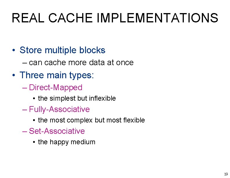
REAL CACHE IMPLEMENTATIONS • Store multiple blocks – can cache more data at once • Three main types: – Direct-Mapped • the simplest but inflexible – Fully-Associative • the most complex but most flexible – Set-Associative • the happy medium 19

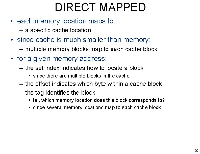
DIRECT MAPPED • each memory location maps to: – a specific cache location • since cache is much smaller than memory: – multiple memory blocks map to each cache block • for a given memory address: – the set index indicates how to locate a block • since there are multiple blocks in the cache – the offset indicates which byte within a cache block – the tag identifies the block • ie. , which memory location does this block corresponds to? • since several memory locations map to each cache block 20

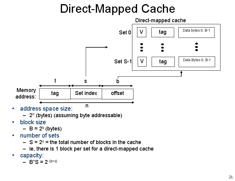
Direct-Mapped Cache Direct-mapped cache Memory address: Set 0 V tag Data bytes 0. . B-1 Set S-1 V tag Data Bytes 0. . B-1 t s b tag Set index offset • address space size: n – 2 n (bytes) (assuming byte addressable) • block size – B = 2 b (bytes) • number of sets – S = 2 s = the total number of blocks in the cache – ie, there is 1 block per set for a direct-mapped cache • capacity: – B*S = 2 (b+s) 21

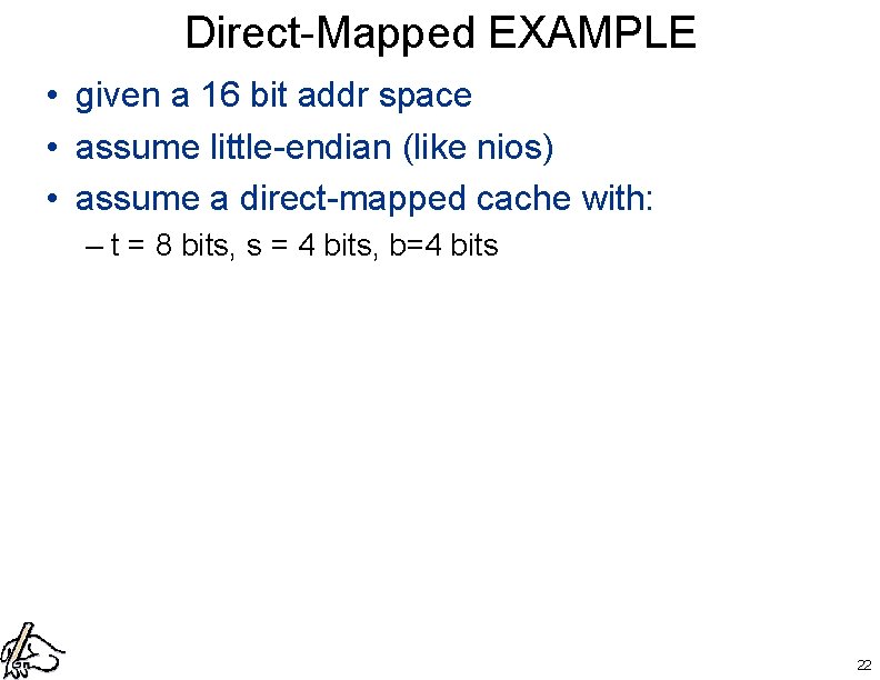
Direct-Mapped EXAMPLE • given a 16 bit addr space • assume little-endian (like nios) • assume a direct-mapped cache with: – t = 8 bits, s = 4 bits, b=4 bits 22

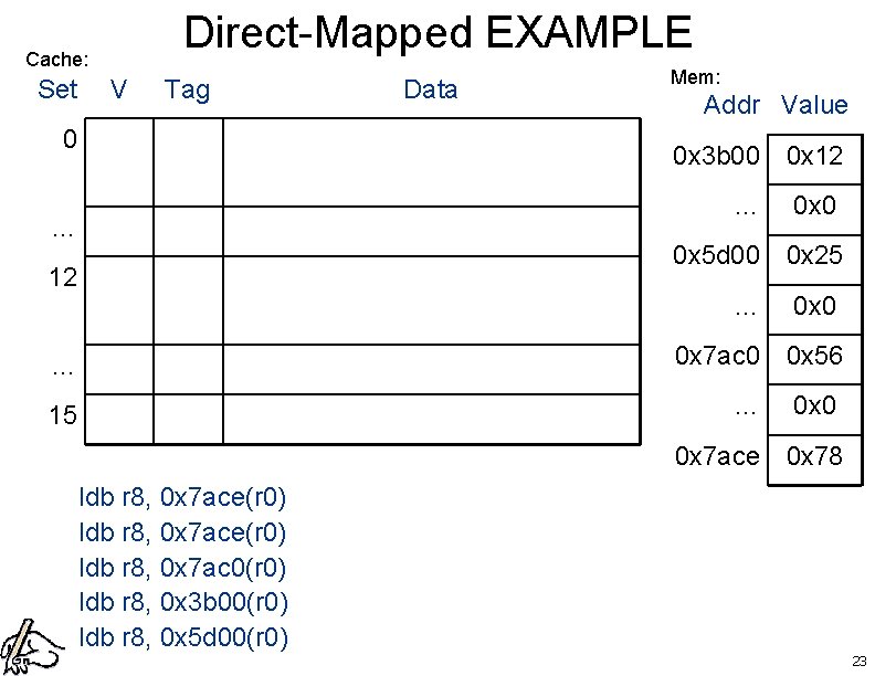
Direct-Mapped EXAMPLE Cache: Set V Tag 0 Data Mem: Addr Value 0 x 3 b 00 0 x 12 … … 0 x 0 0 x 5 d 00 0 x 25 12 … 0 x 0 0 x 7 ac 0 0 x 56 … … 15 0 x 0 0 x 7 ace 0 x 78 ldb r 8, 0 x 7 ace(r 0) ldb r 8, 0 x 7 ac 0(r 0) ldb r 8, 0 x 3 b 00(r 0) ldb r 8, 0 x 5 d 00(r 0) 23

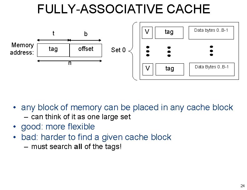
FULLY-ASSOCIATIVE CACHE Memory address: t b tag offset V tag Data bytes 0. . B-1 V tag Data Bytes 0. . B-1 Set 0 n • any block of memory can be placed in any cache block – can think of it as one large set • good: more flexible • bad: harder to find a given cache block – must search all of the tags! 24

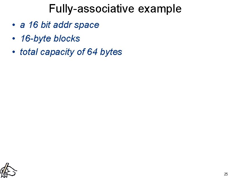
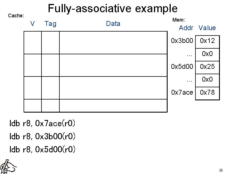
Fully-associative example • a 16 bit addr space • 16 -byte blocks • total capacity of 64 bytes 25

Fully-associative example Cache: V Tag Data Mem: Addr Value 0 x 3 b 00 0 x 12 … 0 x 0 0 x 5 d 00 0 x 25 … 0 x 0 0 x 7 ace 0 x 78 ldb r 8, 0 x 7 ace(r 0) ldb r 8, 0 x 3 b 00(r 0) ldb r 8, 0 x 5 d 00(r 0) 26

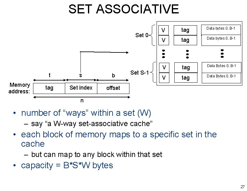
SET ASSOCIATIVE Set 0 Memory address: t s b tag Set index offset V tag Data bytes 0. . B-1 V tag Data Bytes 0. . B-1 Set S-1 n • number of “ways” within a set (W) – say “a W-way set-associative cache” • each block of memory maps to a specific set in the cache – but can map to any block within that set • capacity = B*S*W bytes 27

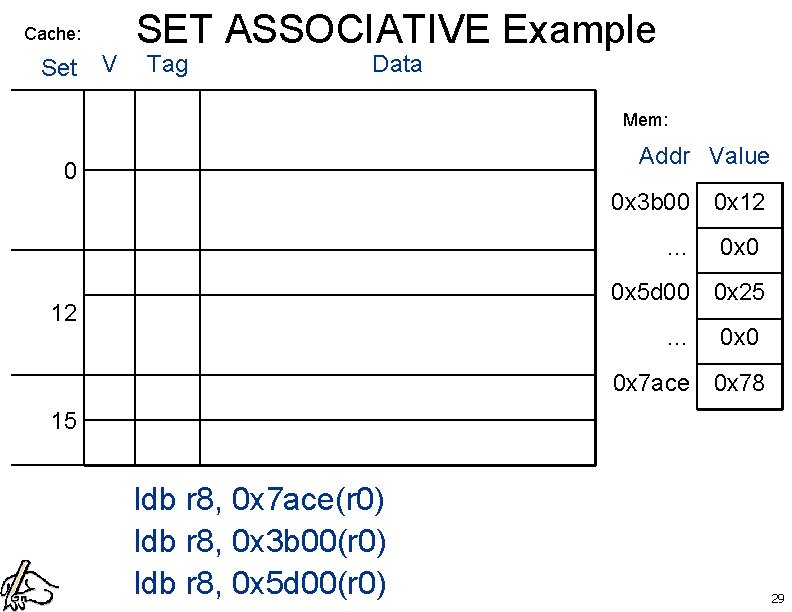
SET ASSOCIATIVE Example • given a 16 bit addr space • assume a 2 -way set-associative cache • t = 8 bits, s = 4 bits, b=4 bits 28

Cache: Set V SET ASSOCIATIVE Example Tag Data Mem: Addr Value 0 0 x 3 b 00 0 x 12 … 0 x 0 0 x 5 d 00 0 x 25 12 … 0 x 0 0 x 7 ace 0 x 78 15 ldb r 8, 0 x 7 ace(r 0) ldb r 8, 0 x 3 b 00(r 0) ldb r 8, 0 x 5 d 00(r 0) 29

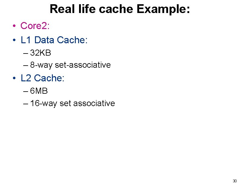
Real life cache Example: • Core 2: • L 1 Data Cache: – 32 KB – 8 -way set-associative • L 2 Cache: – 6 MB – 16 -way set associative 30

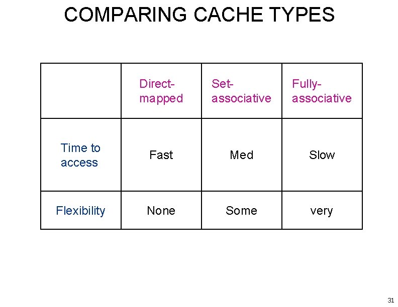
COMPARING CACHE TYPES Directmapped Setassociative Fullyassociative Time to access Fast Med Slow Flexibility None Some very 31

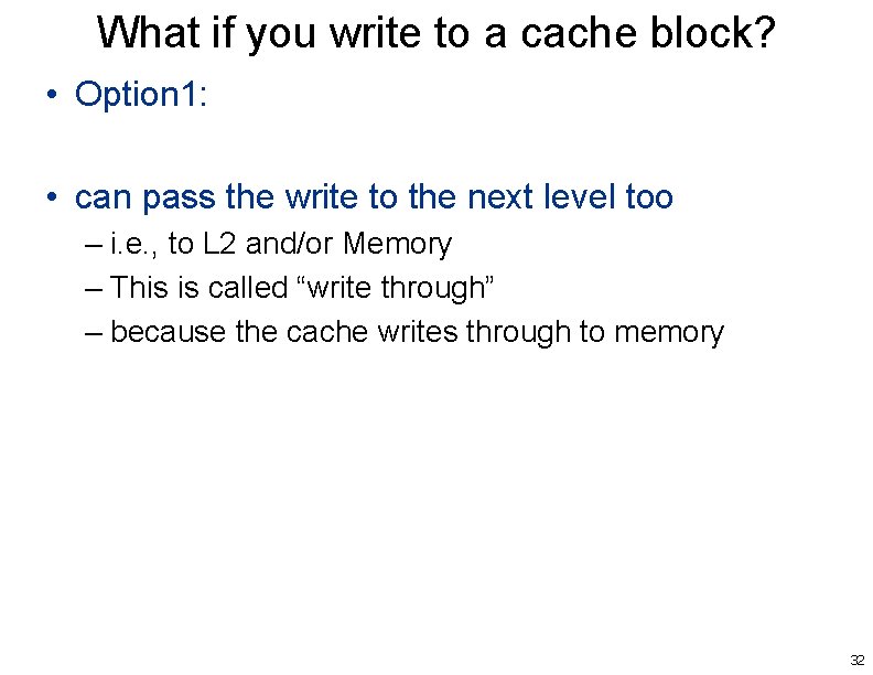
What if you write to a cache block? • Option 1: • can pass the write to the next level too – i. e. , to L 2 and/or Memory – This is called “write through” – because the cache writes through to memory 32

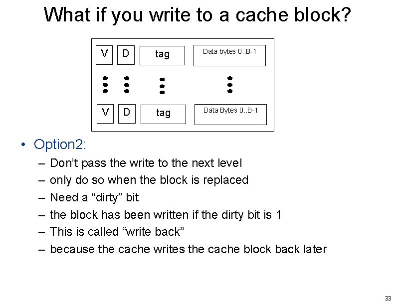
What if you write to a cache block? V D tag Data bytes 0. . B-1 V D tag Data Bytes 0. . B-1 • Option 2: – – – Don’t pass the write to the next level only do so when the block is replaced Need a “dirty” bit the block has been written if the dirty bit is 1 This is called “write back” because the cache writes the cache block back later 33

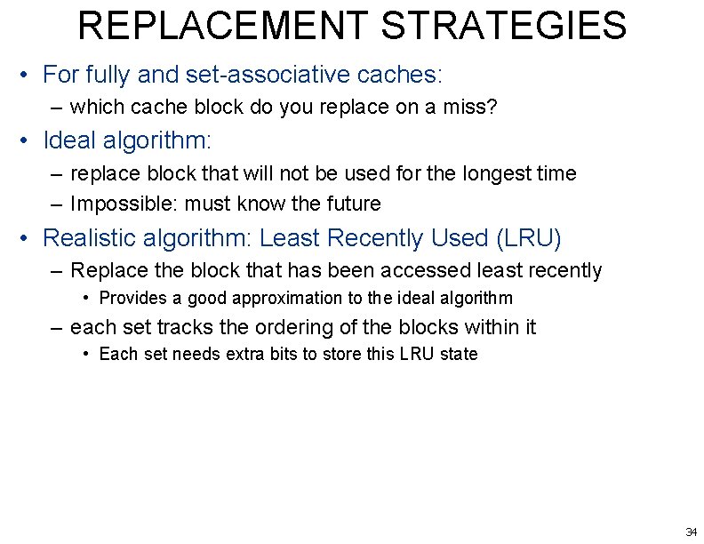
REPLACEMENT STRATEGIES • For fully and set-associative caches: – which cache block do you replace on a miss? • Ideal algorithm: – replace block that will not be used for the longest time – Impossible: must know the future • Realistic algorithm: Least Recently Used (LRU) – Replace the block that has been accessed least recently • Provides a good approximation to the ideal algorithm – each set tracks the ordering of the blocks within it • Each set needs extra bits to store this LRU state 34

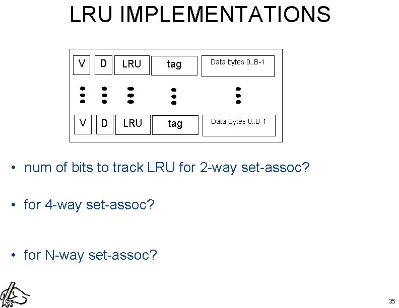
LRU IMPLEMENTATIONS V D LRU tag Data bytes 0. . B-1 V D LRU tag Data Bytes 0. . B-1 • num of bits to track LRU for 2 -way set-assoc? • for 4 -way set-assoc? • for N-way set-assoc? 35

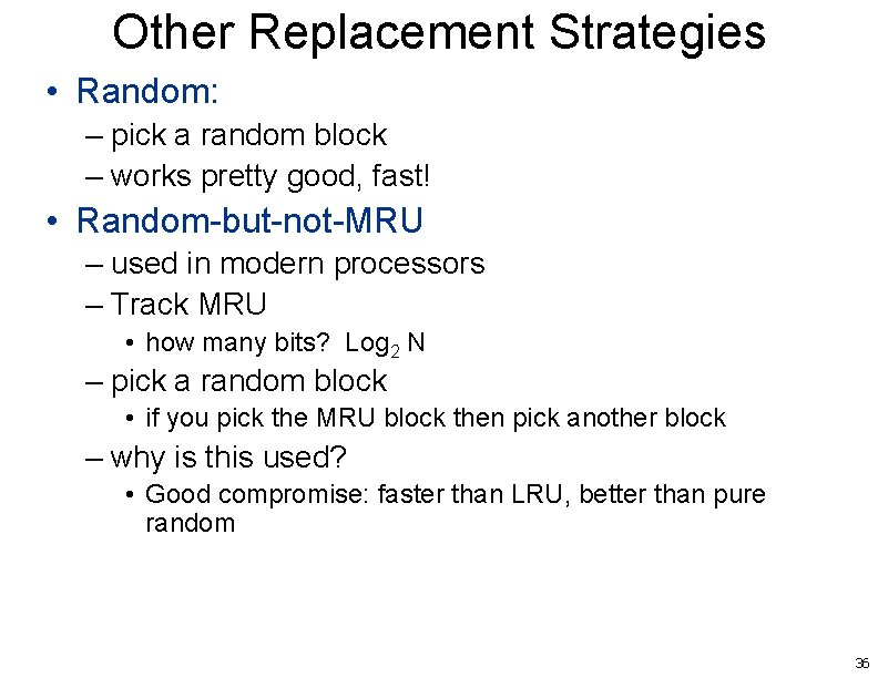
Other Replacement Strategies • Random: – pick a random block – works pretty good, fast! • Random-but-not-MRU – used in modern processors – Track MRU • how many bits? Log 2 N – pick a random block • if you pick the MRU block then pick another block – why is this used? • Good compromise: faster than LRU, better than pure random 36

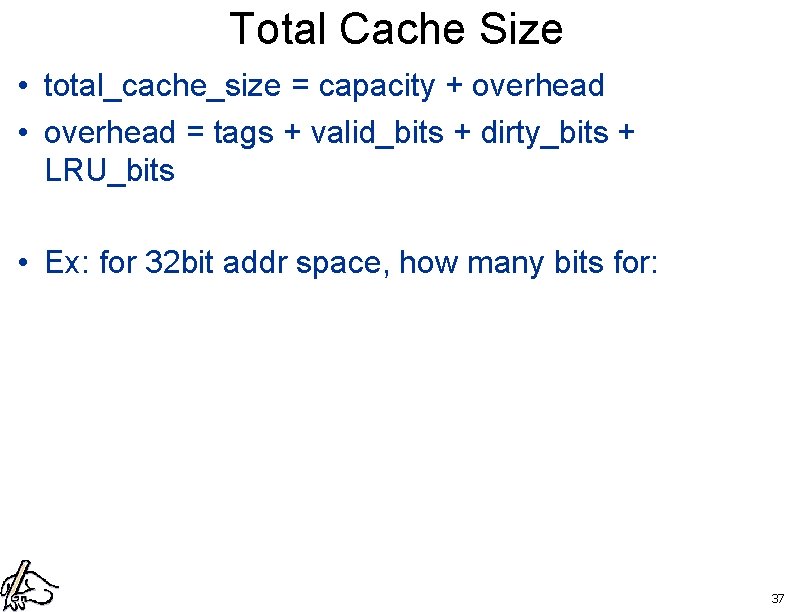
Total Cache Size • total_cache_size = capacity + overhead • overhead = tags + valid_bits + dirty_bits + LRU_bits • Ex: for 32 bit addr space, how many bits for: 37

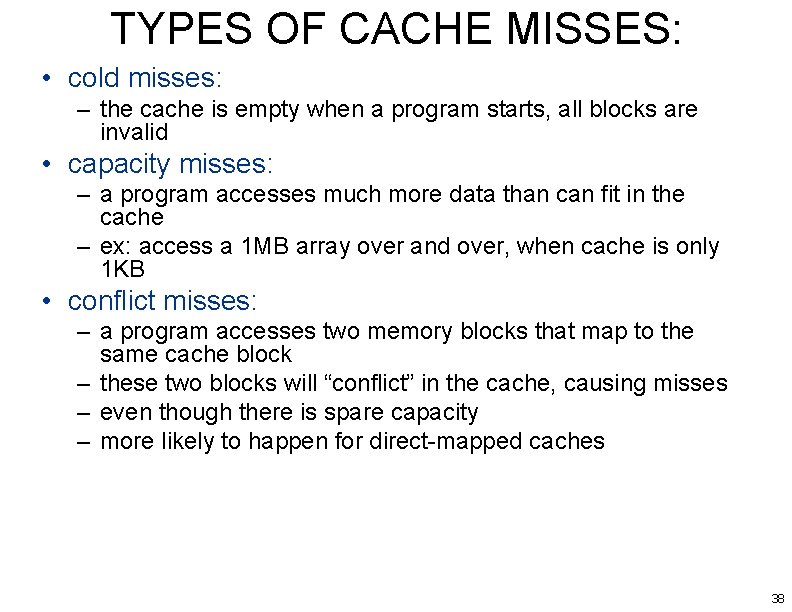
TYPES OF CACHE MISSES: • cold misses: – the cache is empty when a program starts, all blocks are invalid • capacity misses: – a program accesses much more data than can fit in the cache – ex: access a 1 MB array over and over, when cache is only 1 KB • conflict misses: – a program accesses two memory blocks that map to the same cache block – these two blocks will “conflict” in the cache, causing misses – even though there is spare capacity – more likely to happen for direct-mapped caches 38
![Ex ACCESS PATTERNS Assume 1 KB directmapped 32 B blocks Ai Ex: ACCESS PATTERNS • Assume: – – 1 KB direct-mapped 32 B blocks A[i]](https://slidetodoc.com/presentation_image_h/246b8aa72932650634d47fd72bf3e1bf/image-39.jpg)
Ex: ACCESS PATTERNS • Assume: – – 1 KB direct-mapped 32 B blocks A[i] is 4 B cache is cold/empty for (i=0; i<1024; i++){ sum += A[i]; } 39

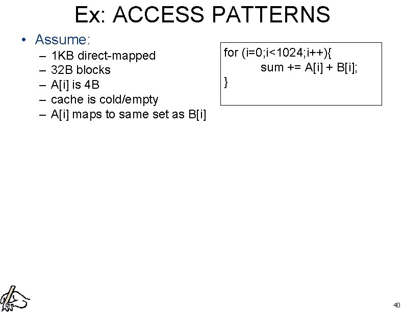
Ex: ACCESS PATTERNS • Assume: – – – 1 KB direct-mapped 32 B blocks A[i] is 4 B cache is cold/empty A[i] maps to same set as B[i] for (i=0; i<1024; i++){ sum += A[i] + B[i]; } 40

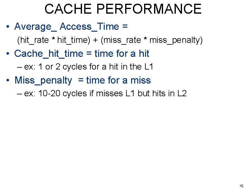
CACHE PERFORMANCE • Average_ Access_Time = (hit_rate * hit_time) + (miss_rate * miss_penalty) • Cache_hit_time = time for a hit – ex: 1 or 2 cycles for a hit in the L 1 • Miss_penalty = time for a miss – ex: 10 -20 cycles if misses L 1 but hits in L 2 41

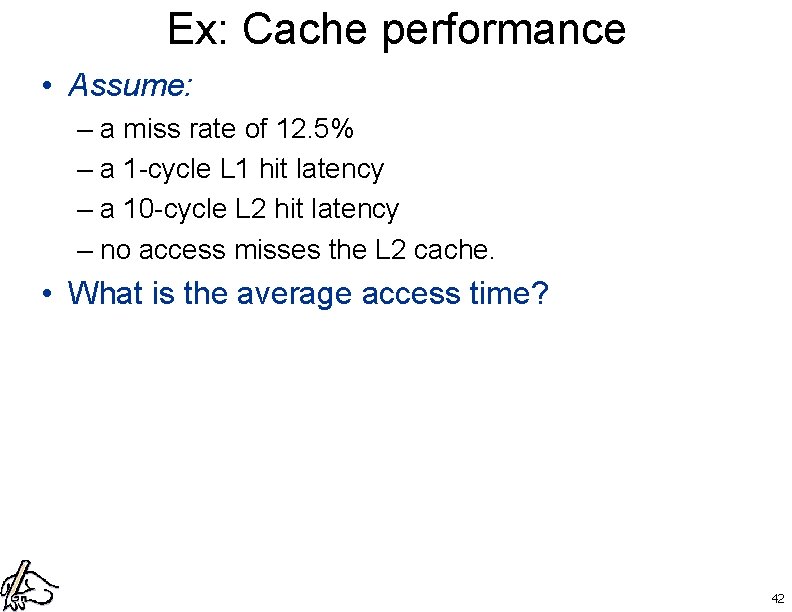
Ex: Cache performance • Assume: – a miss rate of 12. 5% – a 1 -cycle L 1 hit latency – a 10 -cycle L 2 hit latency – no access misses the L 2 cache. • What is the average access time? 42

ECE 243 Memory 43

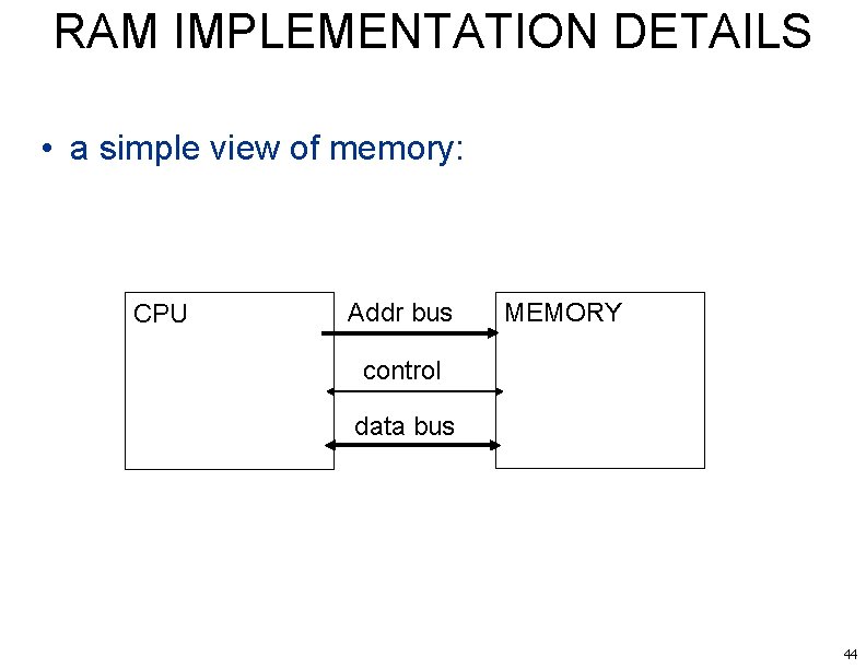
RAM IMPLEMENTATION DETAILS • a simple view of memory: CPU Addr bus MEMORY control data bus 44

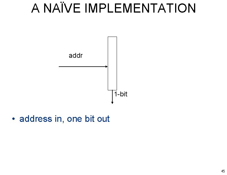
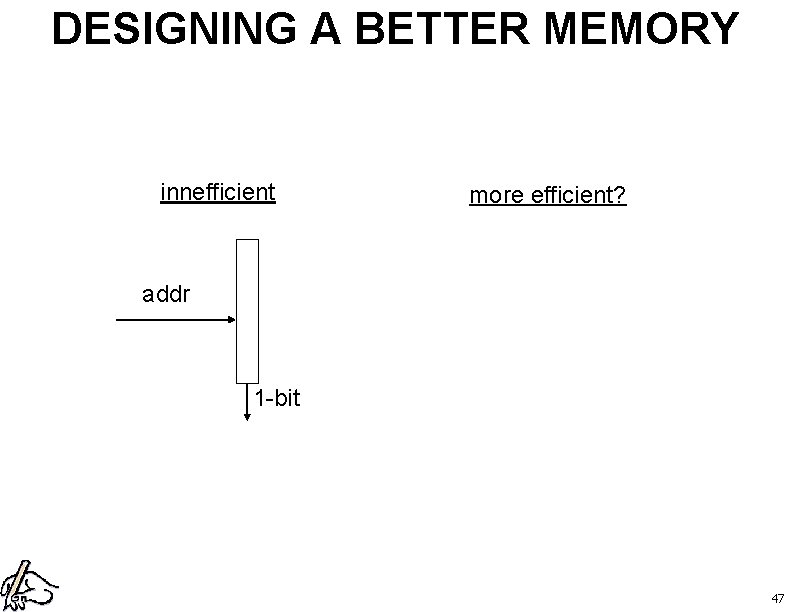
A NAÏVE IMPLEMENTATION addr 1 -bit • address in, one bit out 45

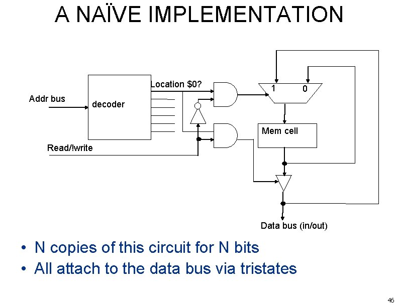
A NAÏVE IMPLEMENTATION Location $0? Addr bus 1 0 decoder Mem cell Read/!write Data bus (in/out) • N copies of this circuit for N bits • All attach to the data bus via tristates 46

DESIGNING A BETTER MEMORY innefficient more efficient? addr 1 -bit 47

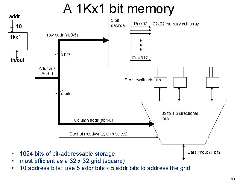
A 1 Kx 1 bit memory addr 5 bit decoder 10 1 kx 1 Row 0? 32 x 32 memory cell array row addr (ab 9 -5) 5 bits Row 31? in/out Addr bus Ab 9 -0 Sense/write circuits 5 bits Column addr (ab 4 -0) 32 to 1 bidirectional mux Control (read/write, chip select) Data in/out (1 bit) • 1024 bits of bit-addressable storage • most efficient as a 32 x 32 grid (square) • 10 address bits: use 5 addr bits x 5 addr bits to address the grid 48

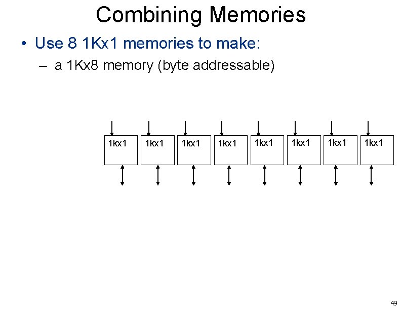
Combining Memories • Use 8 1 Kx 1 memories to make: – a 1 Kx 8 memory (byte addressable) 1 kx 1 1 kx 1 49

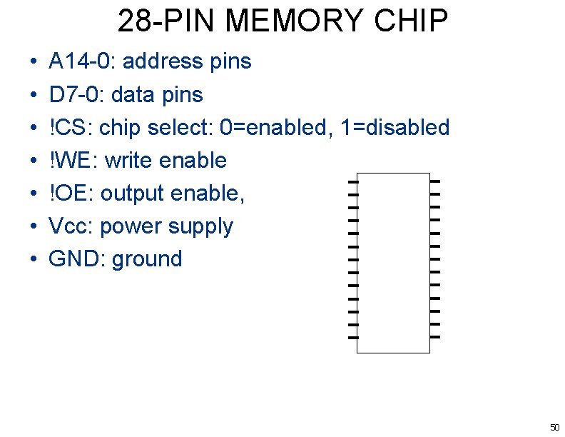
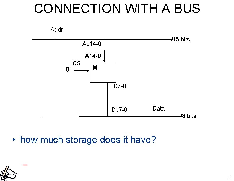
28 -PIN MEMORY CHIP • • A 14 -0: address pins D 7 -0: data pins !CS: chip select: 0=enabled, 1=disabled !WE: write enable !OE: output enable, Vcc: power supply GND: ground 50

CONNECTION WITH A BUS Addr /15 bits Ab 14 -0 A 14 -0 0 !CS M D 7 -0 Db 7 -0 Data /8 bits • how much storage does it have? – 51

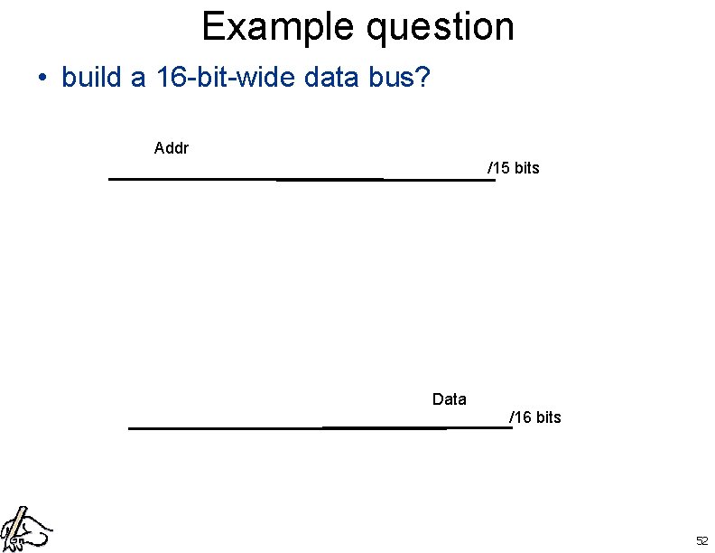
Example question • build a 16 -bit-wide data bus? Addr /15 bits Data /16 bits 52

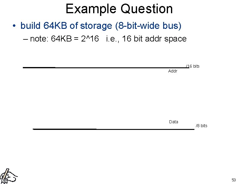
Example Question • build 64 KB of storage (8 -bit-wide bus) – note: 64 KB = 2^16 i. e. , 16 bit addr space /16 bits Addr Data /8 bits 53

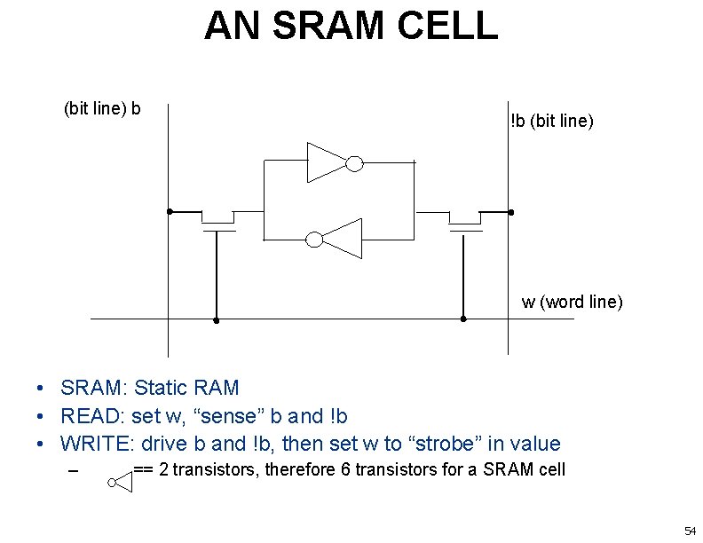
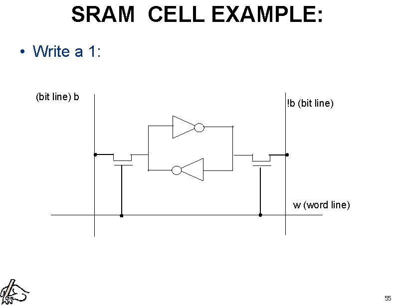
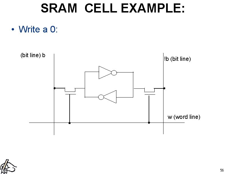
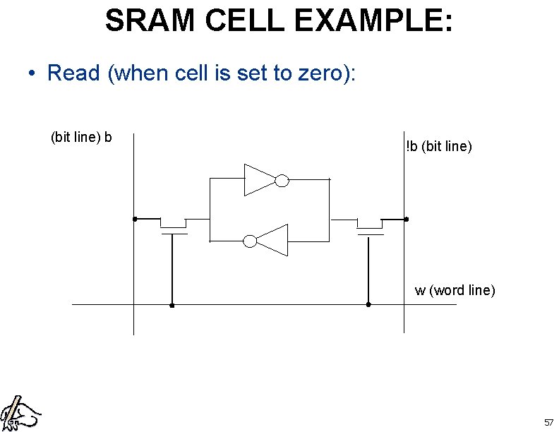
AN SRAM CELL (bit line) b !b (bit line) w (word line) • SRAM: Static RAM • READ: set w, “sense” b and !b • WRITE: drive b and !b, then set w to “strobe” in value – == 2 transistors, therefore 6 transistors for a SRAM cell 54

SRAM CELL EXAMPLE: • Write a 1: (bit line) b !b (bit line) w (word line) 55

SRAM CELL EXAMPLE: • Write a 0: (bit line) b !b (bit line) w (word line) 56

SRAM CELL EXAMPLE: • Read (when cell is set to zero): (bit line) b !b (bit line) w (word line) 57

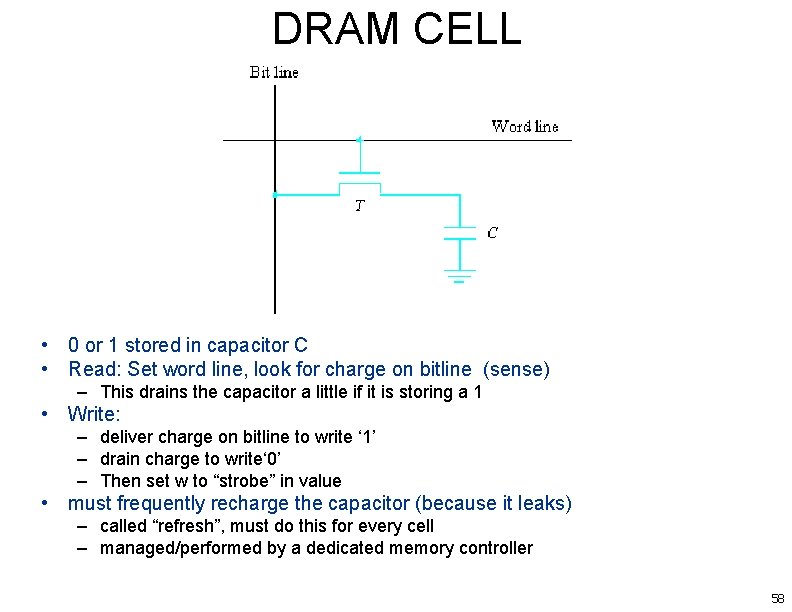
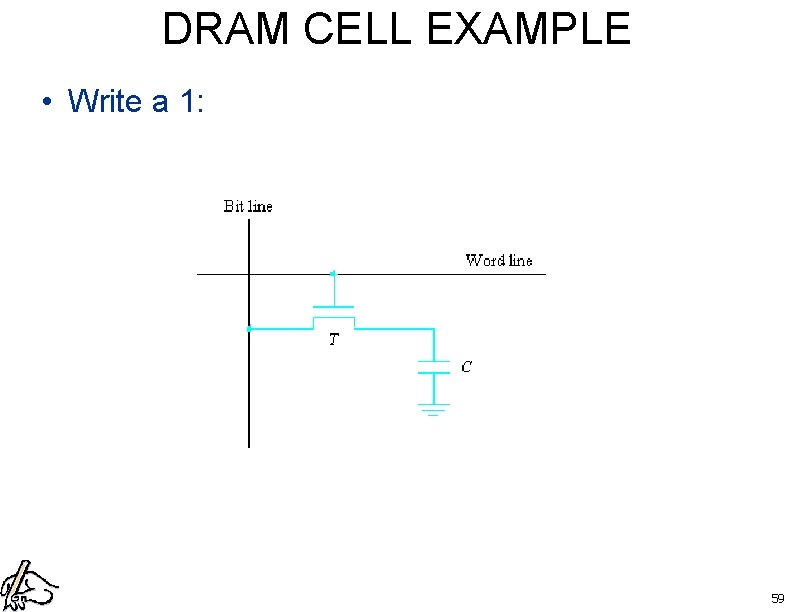
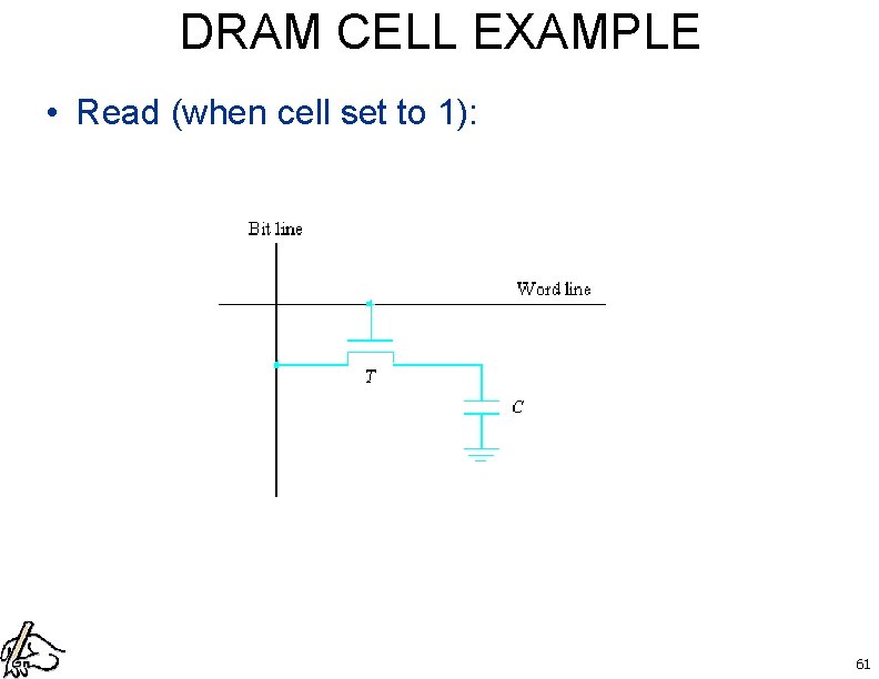
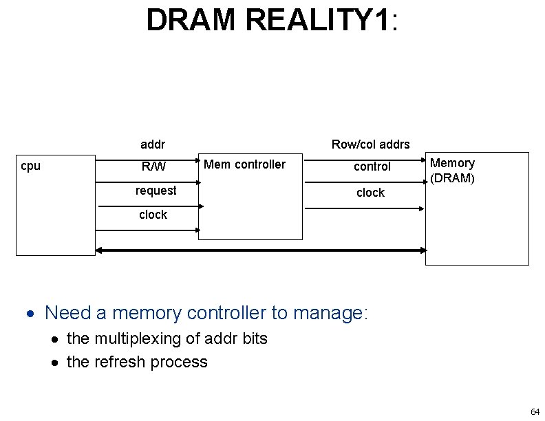
DRAM CELL • 0 or 1 stored in capacitor C • Read: Set word line, look for charge on bitline (sense) – This drains the capacitor a little if it is storing a 1 • Write: – deliver charge on bitline to write ‘ 1’ – drain charge to write‘ 0’ – Then set w to “strobe” in value • must frequently recharge the capacitor (because it leaks) – called “refresh”, must do this for every cell – managed/performed by a dedicated memory controller 58

DRAM CELL EXAMPLE • Write a 1: 59

DRAM CELL EXAMPLE • Write a 0: 60

DRAM CELL EXAMPLE • Read (when cell set to 1): 61

COMPARE SRAM TO DRAM • SRAM: – 6 transistors---expensive – large but fast – no refresh necessary • DRAM: – 1 transistor + 1 capacitor---cheap – small but slower – refresh necessary 62

TYPES OF DRAM • DRAM: – dynamic RAM – asynchronous, needs to be refreshed • SDRAM: – synchronous DRAM • synchronized with a clock signal – Can enter a ‘mode’ to do a “block transfer“ • many bytes with one request from the CPU • DDR-SDRAM: double-data rate SDRAM – Transfer data on both edges of the clock – rather than just the rising edge 63

DRAM REALITY 1: Row/col addrs addr cpu R/W Mem controller request control Memory (DRAM) clock Need a memory controller to manage: the multiplexing of addr bits the refresh process 64

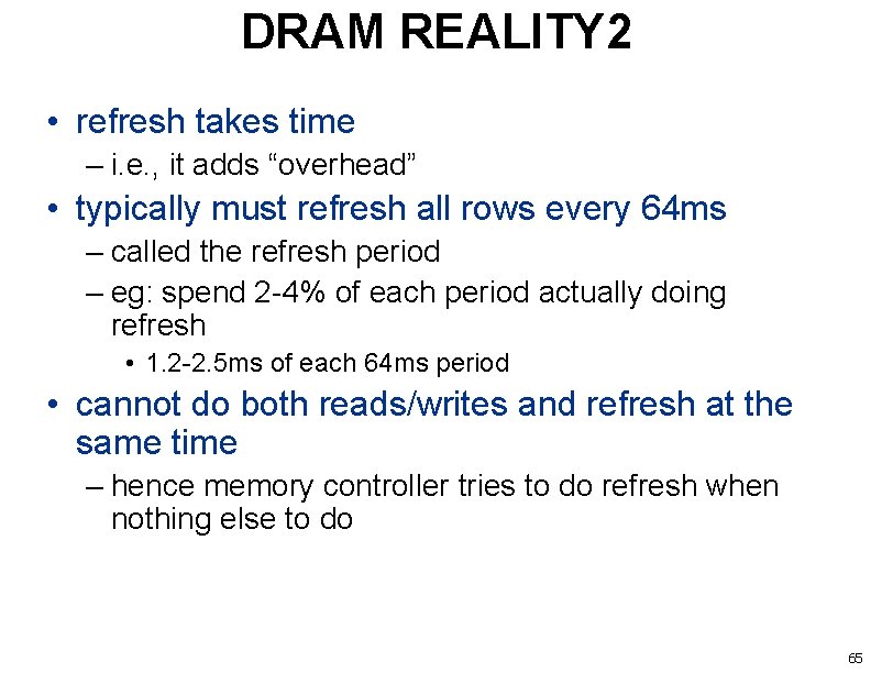
DRAM REALITY 2 • refresh takes time – i. e. , it adds “overhead” • typically must refresh all rows every 64 ms – called the refresh period – eg: spend 2 -4% of each period actually doing refresh • 1. 2 -2. 5 ms of each 64 ms period • cannot do both reads/writes and refresh at the same time – hence memory controller tries to do refresh when nothing else to do 65

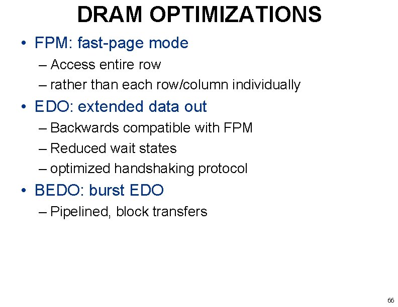
DRAM OPTIMIZATIONS • FPM: fast-page mode – Access entire row – rather than each row/column individually • EDO: extended data out – Backwards compatible with FPM – Reduced wait states – optimized handshaking protocol • BEDO: burst EDO – Pipelined, block transfers 66

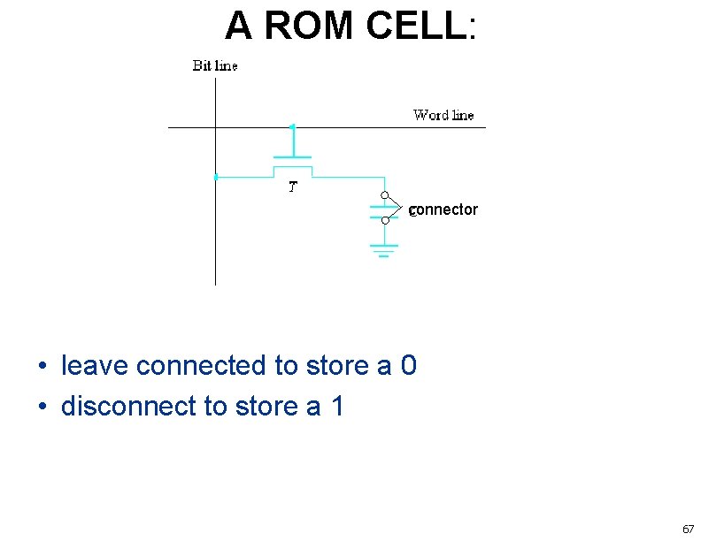
A ROM CELL: connector • leave connected to store a 0 • disconnect to store a 1 67

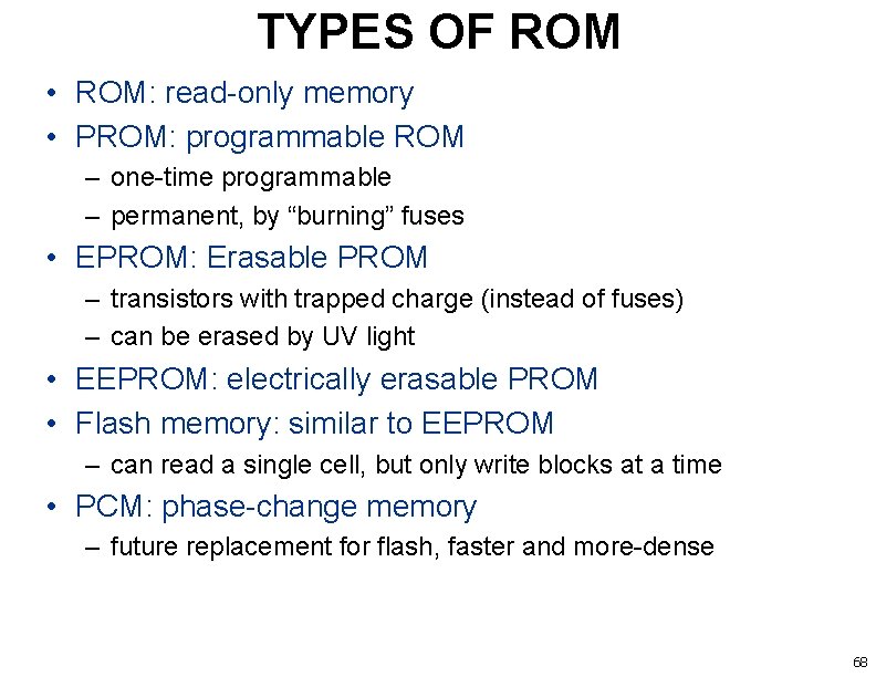
TYPES OF ROM • ROM: read-only memory • PROM: programmable ROM – one-time programmable – permanent, by “burning” fuses • EPROM: Erasable PROM – transistors with trapped charge (instead of fuses) – can be erased by UV light • EEPROM: electrically erasable PROM • Flash memory: similar to EEPROM – can read a single cell, but only write blocks at a time • PCM: phase-change memory – future replacement for flash, faster and more-dense 68

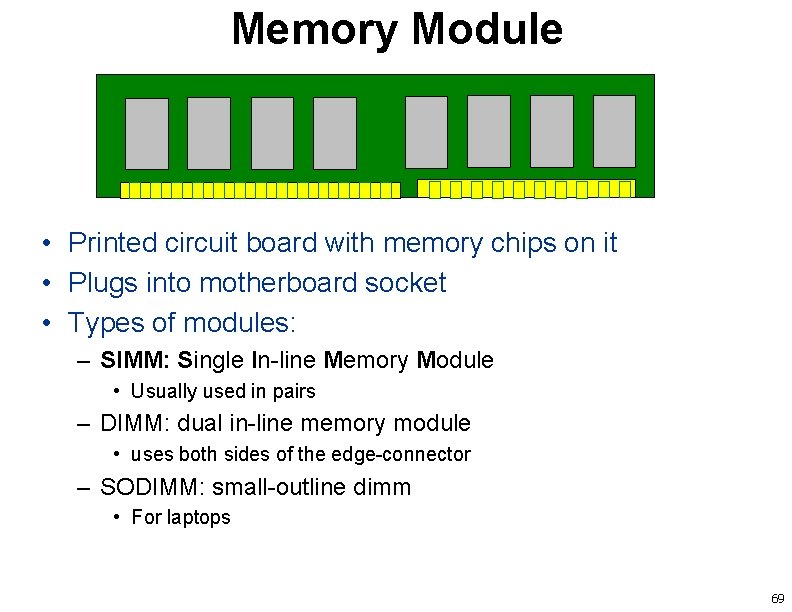
Memory Module • Printed circuit board with memory chips on it • Plugs into motherboard socket • Types of modules: – SIMM: Single In-line Memory Module • Usually used in pairs – DIMM: dual in-line memory module • uses both sides of the edge-connector – SODIMM: small-outline dimm • For laptops 69

ECE 243 Virtual Memory 70

OPERATING SYSTEM (OS) • OS is just a program – with special privileges • implements a file system – using hard-drive – which is just another memory-mapped device • manages devices and drivers – so you don’t have to write assembly for I/O • allows multiple programs to share one CPU – Easy: “context switch” • switch between one program and another • copy all p 1’s registers to a struct in memory • copy all p 2’s state from struct in memory to registers – Hard: • allowing p 1 and p 2 to share the same memory 71

HOW CAN MULTIPLE PROGRAMS SHARE ONE MEM? • i. e. , all of your assembly programs start at memory address 0 x 1000000 – they would all overwrite each other! • Solution: have programs use different parts of memory – But how do you decide who is using which part ahead of time? • Answer: you don’t! – Have the system automatically place programs in separate parts of memory 72

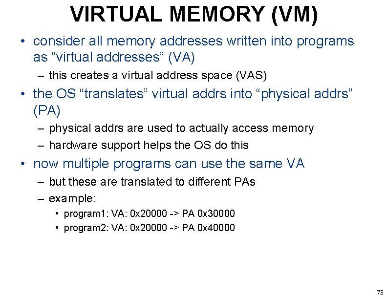
VIRTUAL MEMORY (VM) • consider all memory addresses written into programs as “virtual addresses” (VA) – this creates a virtual address space (VAS) • the OS “translates” virtual addrs into “physical addrs” (PA) – physical addrs are used to actually access memory – hardware support helps the OS do this • now multiple programs can use the same VA – but these are translated to different PAs – example: • program 1: VA: 0 x 20000 -> PA 0 x 30000 • program 2: VA: 0 x 20000 -> PA 0 x 40000 73

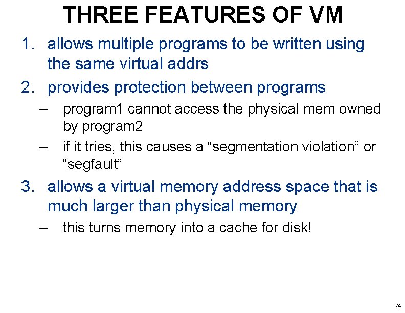
THREE FEATURES OF VM 1. allows multiple programs to be written using the same virtual addrs 2. provides protection between programs – – program 1 cannot access the physical mem owned by program 2 if it tries, this causes a “segmentation violation” or “segfault” 3. allows a virtual memory address space that is much larger than physical memory – this turns memory into a cache for disk! 74

PAGES • OS manages memory in chunks – called “pages” • pages are normally all the same size – normally in the range of 2 KB. . 16 KB – typically 4 KB for most systems • “page fault” – when a required page is not in memory – must transfer page from disk to memory – Similar to a cache miss 75

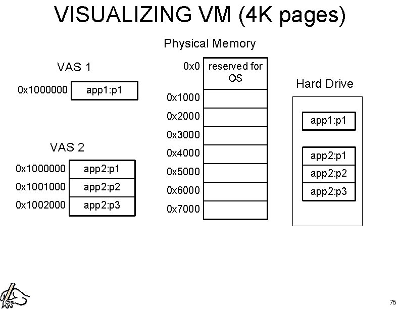
VISUALIZING VM (4 K pages) Physical Memory VAS 1 0 x 1000000 app 1: p 1 0 x 0 reserved for OS Hard Drive 0 x 1000 0 x 2000 app 1: p 1 0 x 3000 VAS 2 0 x 4000 app 2: p 1 0 x 1000000 app 2: p 1 0 x 5000 app 2: p 2 0 x 1001000 app 2: p 2 0 x 6000 app 2: p 3 0 x 1002000 app 2: p 3 0 x 7000 76

VM QUESTION • Virtual Memory – effectively turns RAM into a cache for hard drive – with page-sized “cache-blocks” • What is the associativity of this ‘cache’? 77

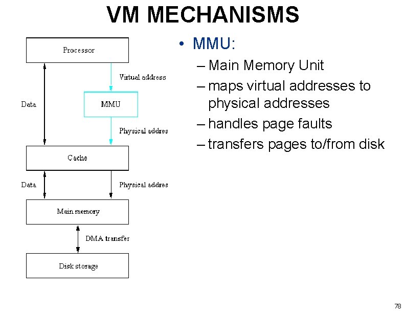
VM MECHANISMS • MMU: – Main Memory Unit – maps virtual addresses to physical addresses – handles page faults – transfers pages to/from disk 78

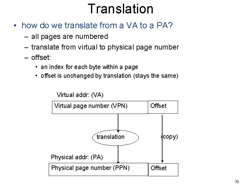
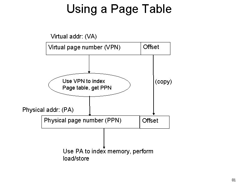
Translation • how do we translate from a VA to a PA? – all pages are numbered – translate from virtual to physical page number – offset: • an index for each byte within a page • offset is unchanged by translation (stays the same) Virtual addr: (VA) Virtual page number (VPN) translation Offset (copy) Physical addr: (PA) Physical page number (PPN) Offset 79

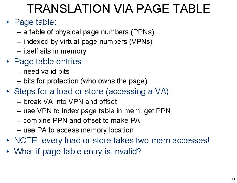
TRANSLATION VIA PAGE TABLE • Page table: – a table of physical page numbers (PPNs) – indexed by virtual page numbers (VPNs) – itself sits in memory • Page table entries: – need valid bits – bits for protection (who owns the page) • Steps for a load or store (accessing a VA): – – break VA into VPN and offset use VPN to index page table in mem, get PPN combine PPN and offset to make PA use PA to access memory location • NOTE: every load or store takes two mem accesses! • What if page table entry is invalid? 80

Using a Page Table Virtual addr: (VA) Virtual page number (VPN) Use VPN to index Page table, get PPN Offset (copy) Physical addr: (PA) Physical page number (PPN) Offset Use PA to index memory, perform load/store 81

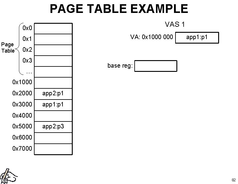
PAGE TABLE EXAMPLE VAS 1 0 x 0 Page Table VA: 0 x 1000 0 x 1 app 1: p 1 0 x 2 0 x 3 base reg: … 0 x 1000 0 x 2000 app 2: p 1 0 x 3000 app 1: p 1 0 x 4000 0 x 5000 app 2: p 3 0 x 6000 0 x 7000 82

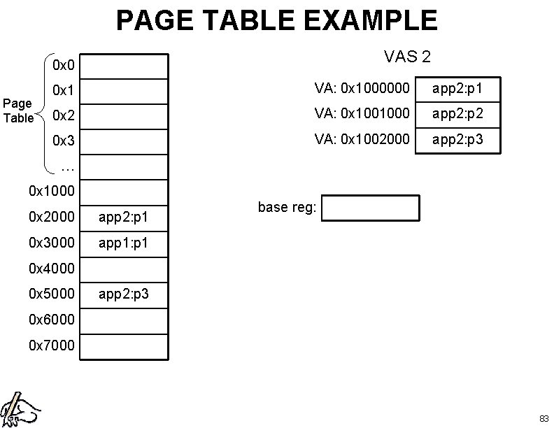
PAGE TABLE EXAMPLE VAS 2 0 x 0 Page Table 0 x 1 VA: 0 x 1000000 app 2: p 1 0 x 2 VA: 0 x 1001000 app 2: p 2 0 x 3 VA: 0 x 1002000 app 2: p 3 … 0 x 1000 0 x 2000 app 2: p 1 0 x 3000 app 1: p 1 base reg: 0 x 4000 0 x 5000 app 2: p 3 0 x 6000 0 x 7000 83

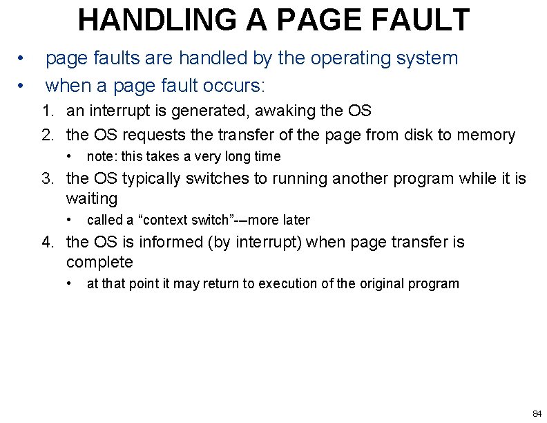
HANDLING A PAGE FAULT • • page faults are handled by the operating system when a page fault occurs: 1. an interrupt is generated, awaking the OS 2. the OS requests the transfer of the page from disk to memory • note: this takes a very long time 3. the OS typically switches to running another program while it is waiting • called a “context switch”---more later 4. the OS is informed (by interrupt) when page transfer is complete • at that point it may return to execution of the original program 84

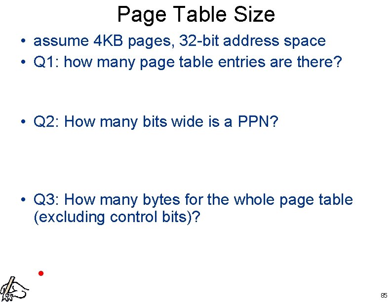
Page Table Size • assume 4 KB pages, 32 -bit address space • Q 1: how many page table entries are there? • Q 2: How many bits wide is a PPN? • Q 3: How many bytes for the whole page table (excluding control bits)? 85

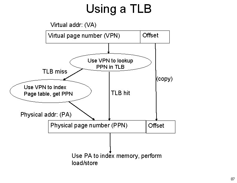
Translation Lookaside Buffer (TLB) • Page table is quite large – And must be accessed for every mem reference! • Exploit locality: – Only using a small subset of pages at any time – Keep a small cache of in-use page table entries • TLB: – a small, fully-assoc cache of page table entries – integrated into and managed by the MMU 86

Using a TLB Virtual addr: (VA) Virtual page number (VPN) Offset Use VPN to lookup PPN in TLB miss (copy) Use VPN to index Page table, get PPN TLB hit Physical addr: (PA) Physical page number (PPN) Offset Use PA to index memory, perform load/store 87

ECE 243 Disks 88

HARD DRIVES • can store tens to hundreds of GB • on the order of milliseconds to read – 100, 000 X slower than DRAM – 1, 000 X slower than SRAM 89

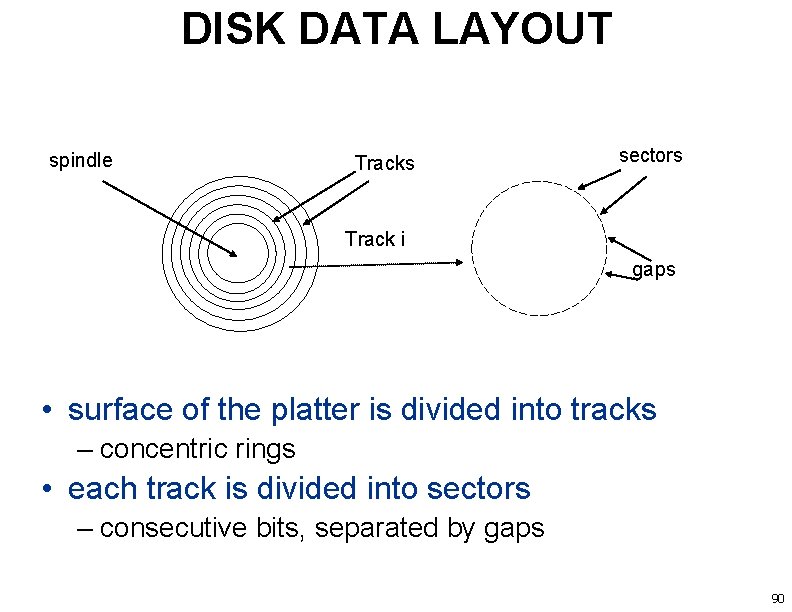
DISK DATA LAYOUT spindle Tracks sectors Track i gaps • surface of the platter is divided into tracks – concentric rings • each track is divided into sectors – consecutive bits, separated by gaps 90

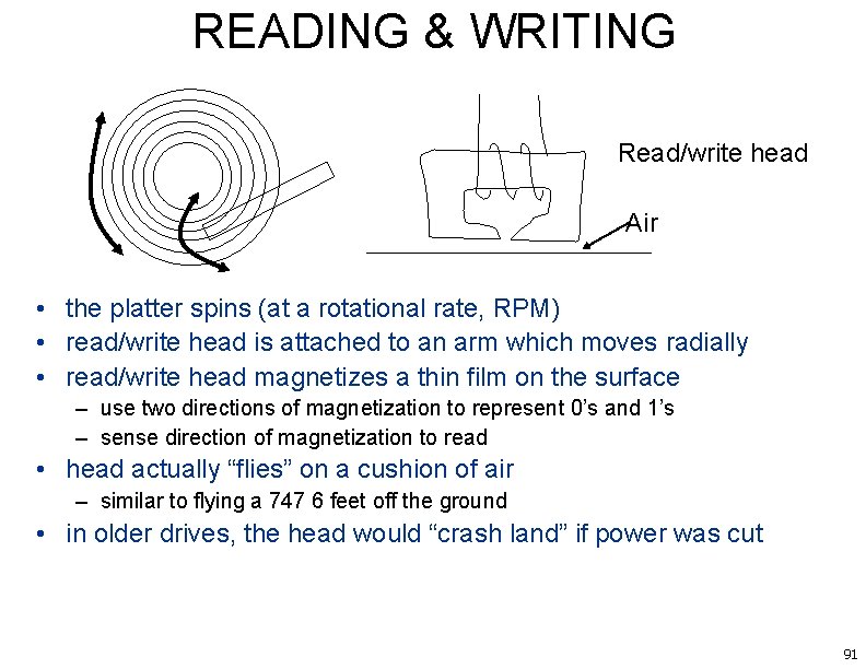
READING & WRITING Read/write head Air • the platter spins (at a rotational rate, RPM) • read/write head is attached to an arm which moves radially • read/write head magnetizes a thin film on the surface – use two directions of magnetization to represent 0’s and 1’s – sense direction of magnetization to read • head actually “flies” on a cushion of air – similar to flying a 747 6 feet off the ground • in older drives, the head would “crash land” if power was cut 91

DISK ARCHITECTURES • can have one arm with two read/write heads – to read/write both upper and lower surfaces of platter • can have multiple platters and arms • Disk capacity = – #bytes/sector * avg_#_sectors/track * #tracks/surface * #surfaces/platter * #platters/disk • why is there an “average” number of sectors per track? – 92

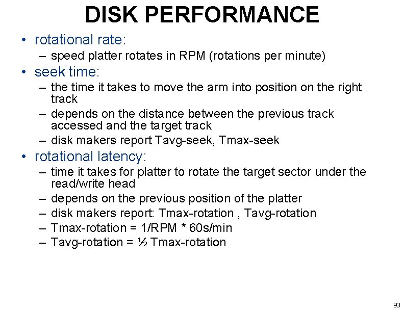
DISK PERFORMANCE • rotational rate: – speed platter rotates in RPM (rotations per minute) • seek time: – the time it takes to move the arm into position on the right track – depends on the distance between the previous track accessed and the target track – disk makers report Tavg-seek, Tmax-seek • rotational latency: – time it takes for platter to rotate the target sector under the read/write head – depends on the previous position of the platter – disk makers report: Tmax-rotation , Tavg-rotation – Tmax-rotation = 1/RPM * 60 s/min – Tavg-rotation = ½ Tmax-rotation 93

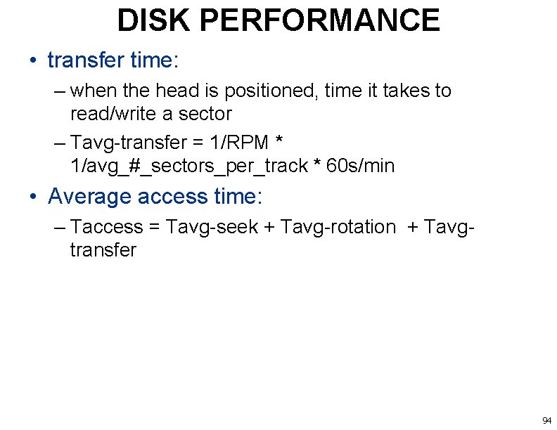
DISK PERFORMANCE • transfer time: – when the head is positioned, time it takes to read/write a sector – Tavg-transfer = 1/RPM * 1/avg_#_sectors_per_track * 60 s/min • Average access time: – Taccess = Tavg-seek + Tavg-rotation + Tavgtransfer 94

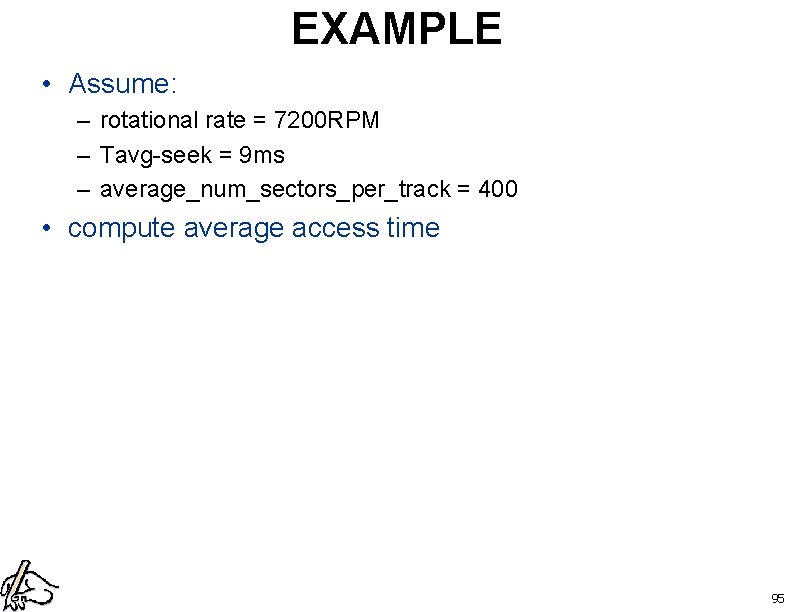
EXAMPLE • Assume: – rotational rate = 7200 RPM – Tavg-seek = 9 ms – average_num_sectors_per_track = 400 • compute average access time 95

DISK REALITY • to hide complexity of sectors/tracks/rotation etc: – disk presents view of “logical blocks” – each block is the size of a sector – and numbered 0. . B-1 for all B sectors on the disk • disks must be formatted: – info added in gaps that identify sectors – mark bad sectors • disk connected to the system bus through a “disk controller” – can transfer data in blocks between memory and disk – larger than cache blocks – called DMA “direct memory access” 96

REAL HARD DISK TYPES • ATA/EIDE: advanced technology attachment / enhanced integrated drive electronics – – IDE and ATA are the same thing, IDE is a marketing term Can connect directly to PCI bus Can connect directly to some Pentium motherboards SATA: serial ATA • SCSI: (pronounced scuzzy): – attaches to SCSI bus, can be faster than drives attached to PCI bus • RAID: Redundant Array of Inexpensive Disks – Rather than one big expensive disk, have several inexpensive disks – Can break a single file up (called striping) into parts (called “stripes”) • Put each stripe on a separate disk • Now can read one file faster (read many disks at once) – Can also replicate data on the disks to improve reliability • Ie. , if one disk fails, another is there as a backup 97

OPTICAL DISKS • CDs: Compact Disks – Uses a laser to read indentations (pits) on disk – Disks may contain errors (doesn’t really matter for audio) • CD-ROM: – like a CD, but has error checking (so can use for computer data) • CD-R: (recordable) – can write once by using laser to burn pits • CD-Re. Writable: – can be written multiple times, similar to CD-R • DVD: digital versatile disk: – like CD, but shorter-wavelength laser, smaller pits, more dense tracks • DVD-R: writable DVD • DVD-RW: rewritable DVD 98

Final Note • Flash memory and similar technologies – are quickly replacing hard drives – ex: can buy laptops with flash-like storage • no hard drive – saves power, size, weight • Downside: – flash wears out (current tech) – need clever algorithms to “spread accesses” – system might tell you to replace your drive 99