ECE 4430 Project Presentation OPERATIONAL AMPLIFIER GROUP 3
- Slides: 21
ECE 4430 Project Presentation OPERATIONAL AMPLIFIER GROUP 3 – DEBASHIS BANERJEE JASON PINTO ASHITA MATHEW
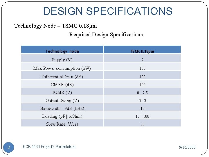
DESIGN SPECIFICATIONS Technology Node – TSMC 0. 18µm Required Design Specifications 2 Technology node TSMC 0. 18µm Supply (V) 2 Max Power consumption (u. W) 150 Differential Gain (d. B) 100 CMRR (d. B) 100 ICMR (V) 0 - 2. 5 Output Swing (V) 0 -2 Bandwidth - 3 d. B (k. Hz) 10 Loading (p. F || k. Ohm) 10 || 100 Slew Rate (V/us) 20 ECE 4430 Project 2 Presentation 9/16/2020
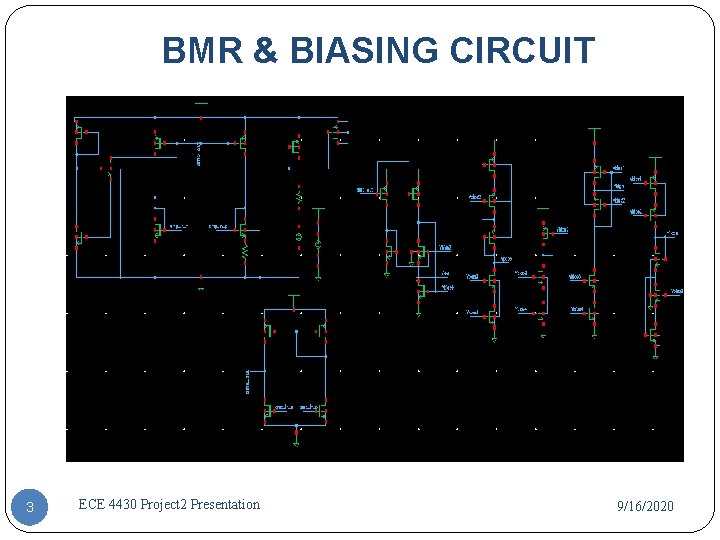
BMR & BIASING CIRCUIT 3 ECE 4430 Project 2 Presentation 9/16/2020
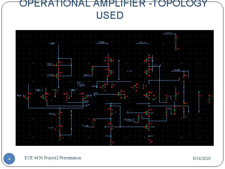
OPERATIONAL AMPLIFIER -TOPOLOGY USED 4 ECE 4430 Project 2 Presentation 9/16/2020
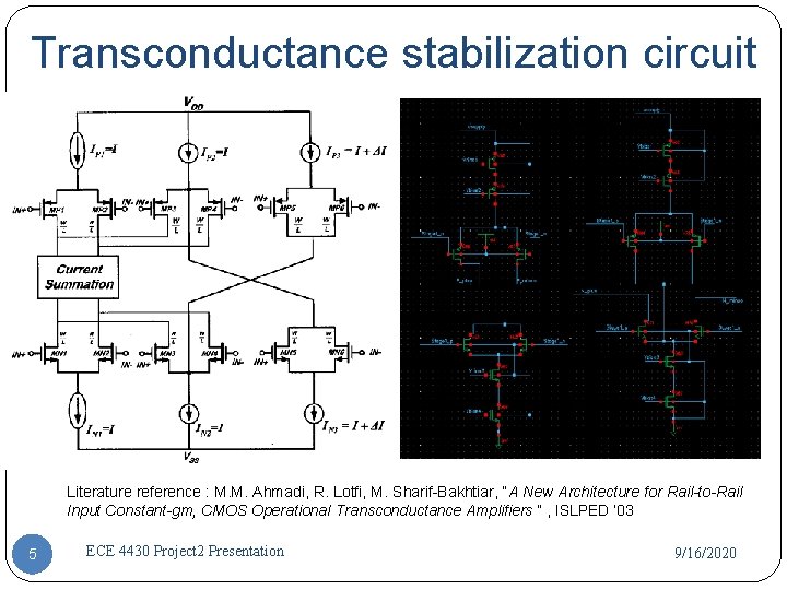
Transconductance stabilization circuit Literature reference : M. M. Ahmadi, R. Lotfi, M. Sharif-Bakhtiar, “A New Architecture for Rail-to-Rail Input Constant-gm, CMOS Operationa. I Transconductance Amplifiers ” , ISLPED ‘ 03 5 ECE 4430 Project 2 Presentation 9/16/2020
INITIAL DESIGN STEPS Redesigned BMR with 5 u. A reference current Designed short channel biasing circuit Total current budget = 75 u. A for a max power consumption of 150 u. W The transconductances of the PMOS NMOS pair of amplifying devices 6 were made equal by sizing the PMOS to NMOS in the ratio kpn: kpp (5: 1) Current combining stage is made low voltage headroom cascode with floating current sources for proper biasing. The transconductance stage of diffamp was biased with 5 u. A each and the summing stage was designed for a current of 30 u. A For a rail to rail output swing, we designed a class AB push pull amplifier Using CC= 0. 22 CL caused the bandwidth to be about 100 Hz only. Compensation capacitor was fine tuned iteratively to achieve a desired phase margin and maximum bandwidth possible. ECE 4430 Project 2 Presentation 9/16/2020
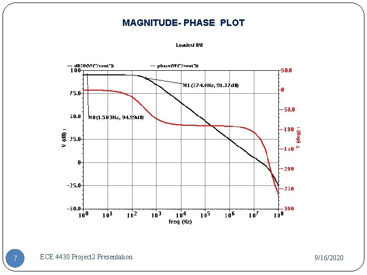
MAGNITUDE- PHASE PLOT 7 ECE 4430 Project 2 Presentation 9/16/2020
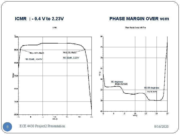
ICMR : - 0. 4 V to 2. 23 V 90. 32 d. B, -0. 41 V PHASE MARGIN OVER vcm 90. 32 d. B, 2. 23 V 56 degrees 50. 09 degrees 8 ECE 4430 Project 2 Presentation 9/16/2020
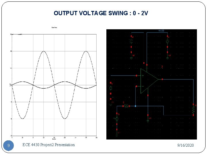
OUTPUT VOLTAGE SWING : 0 - 2 V -0. 25 V , 93 d. B 90. 32 d. B, -0. 41 V 9 ECE 4430 Project 2 Presentation 2. 25 V, 88 d. B 90. 32 d. B, 2. 23 V 9/16/2020
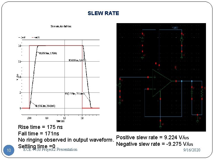
SLEW RATE 10 Rise time = 175 ns Fall time = 171 ns No ringing observed in output waveform. Positive slew rate = 9. 224 V/us Negative slew rate = -9. 275 V/us Settling time =0 ECE 4430 Project 2 Presentation 9/16/2020
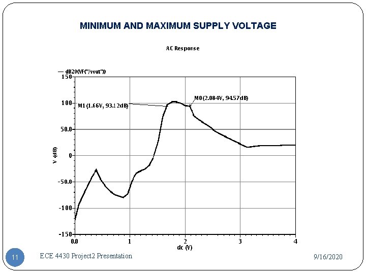
MINIMUM AND MAXIMUM SUPPLY VOLTAGE 11 ECE 4430 Project 2 Presentation 9/16/2020
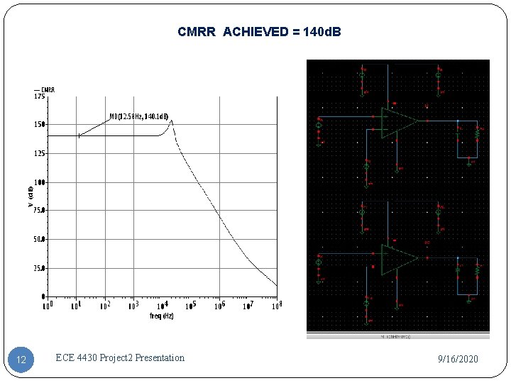
CMRR ACHIEVED = 140 d. B 12 ECE 4430 Project 2 Presentation 9/16/2020
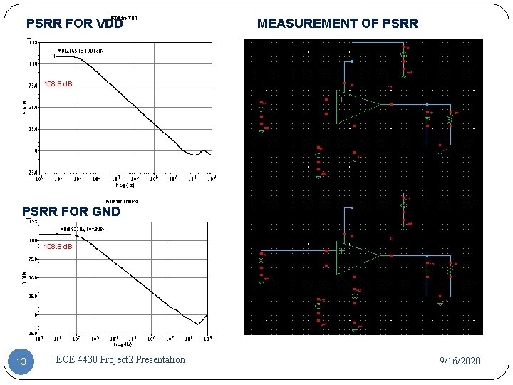
PSRR FOR VDD MEASUREMENT OF PSRR 108. 8 d. B PSRR FOR GND 108. 8 d. B 13 ECE 4430 Project 2 Presentation 9/16/2020
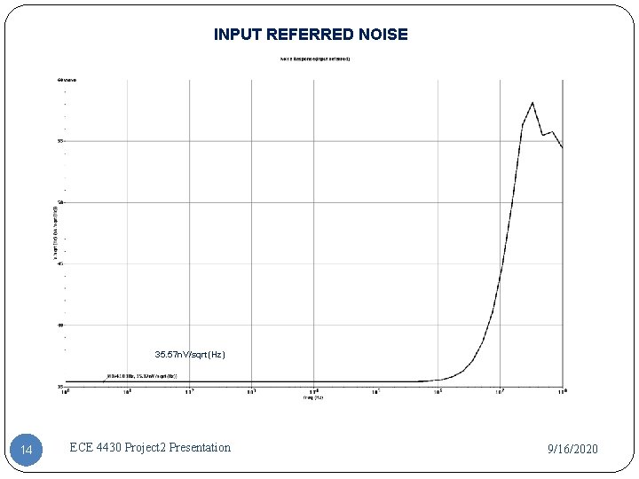
INPUT REFERRED NOISE 35. 57 n. V/sqrt(Hz) 14 ECE 4430 Project 2 Presentation 9/16/2020
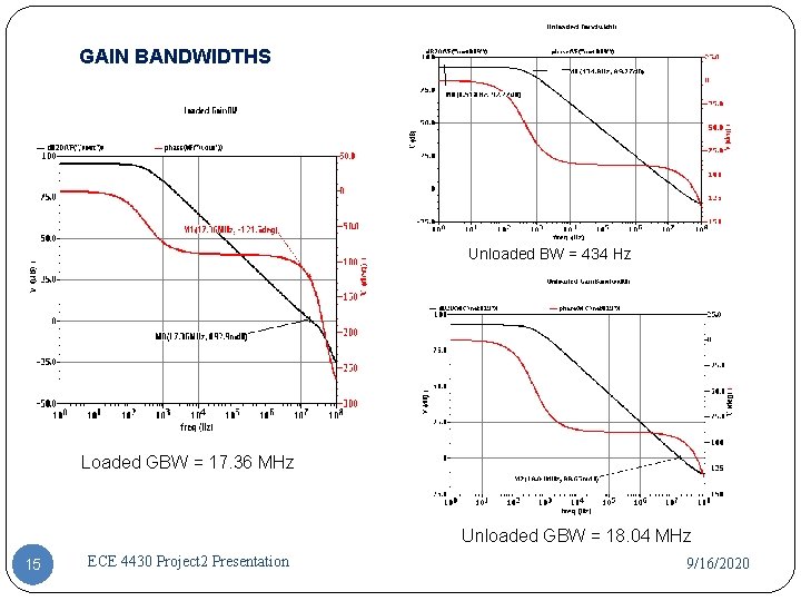
GAIN BANDWIDTHS Unloaded BW = 434 Hz Loaded GBW = 17. 36 MHz Unloaded GBW = 18. 04 MHz 15 ECE 4430 Project 2 Presentation 9/16/2020
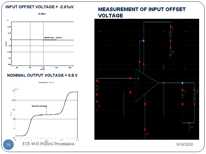
INPUT OFFSET VOLTAGE = -2. 01 u. V MEASUREMENT OF INPUT OFFSET VOLTAGE NOMINAL OUTPUT VOLTAGE = 0. 8 V 16 ECE 4430 Project 2 Presentation 9/16/2020
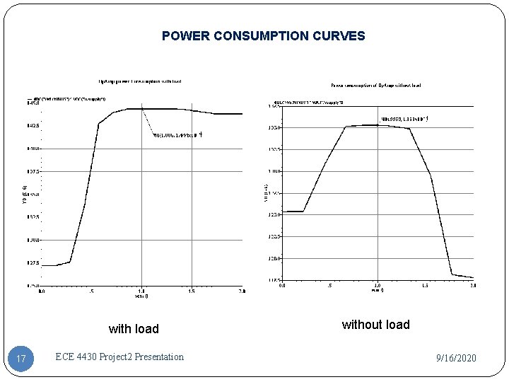
POWER CONSUMPTION CURVES with load 17 ECE 4430 Project 2 Presentation without load 9/16/2020
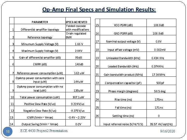
Op-Amp Final Specs and Simulation Results: PARAMETER 1 Differential amplifier topology 2 Reference topology SPECS ACHEIVED Folded cascode with modifications Drain regulated BMR 3 Minumum Supply Voltage (V) 1. 66 V 4 Maximum Supply Voltage (V) 2. 84 V 18 Input offset voltage (m. V) 0. 002 m. V 5 Gain of differential amplifier (d. B) 95 d. B 19 Unloaded Bandwidth (k. Hz) 0. 434 KHz 6 CMRR (d. B) 140 d. B 20 Loaded Bandwidth (k. Hz) 0. 374 KHz 21 Gain bandwidth product (MHz) 17. 36 MHz 22 Compensation capacitor (p. F) 500 p. F 23 Phase margin (degrees) 58. 5 deg 24 Rise time (ns) 175 ns 25 Fall time (ns) 171 ns 26 Settling time (ns) 7 Reference power consumption (u. W) 8 162 u. W Op. Amp power consumption with zero 144 u. W input (u. W) Op. Amp power consumption with no 135 u. W load (u. W) 9 18 10 Total power consumption (u. W) 307. 1 u. W 11 Positive Slew Rate (V/us) 9. 224 V/us 12 Negative Slew Rate (V/us) -9. 275 V/us 13 ICMR (Vmin ~ Vmax) -0. 4 V – 2. 23 V 14 Output Swing (Vmin ~ Vmax) 0 -2 V ECE 4430 Project 2 Presentation 15 VDD PSRR (d. B) 108. 8 d. B 16 GND PSRR (d. B) 108. 8 d. B 17 Nominal output voltage (V) Input referred noise (V/Hz^0. 5) 0. 8 V 0 35. 57 n. V/sqrt(Hz) 9/16/2020
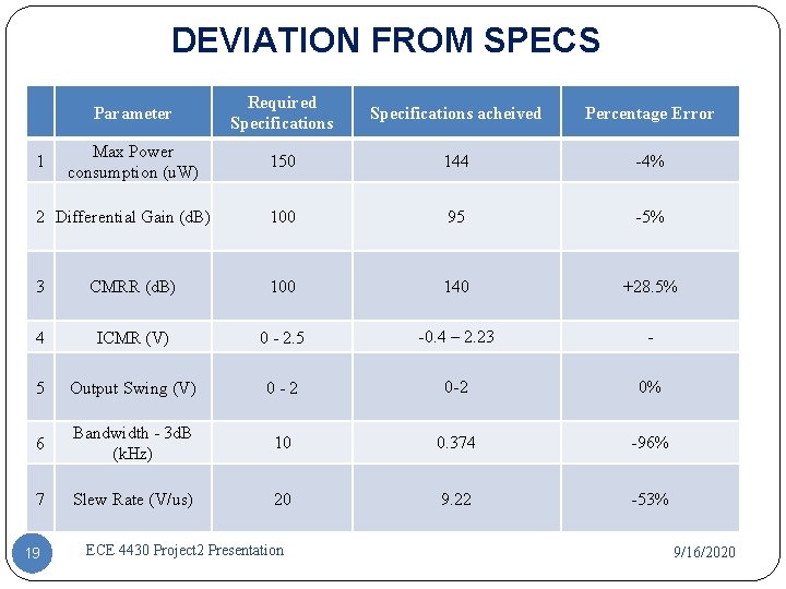
DEVIATION FROM SPECS Parameter Required Specifications acheived Percentage Error Max Power consumption (u. W) 150 144 -4% 2 Differential Gain (d. B) 100 95 -5% 3 CMRR (d. B) 100 140 +28. 5% 4 ICMR (V) 0 - 2. 5 -0. 4 – 2. 23 - 5 Output Swing (V) 0 -2 0% 6 Bandwidth - 3 d. B (k. Hz) 10 0. 374 -96% 7 Slew Rate (V/us) 20 9. 22 -53% 1 19 ECE 4430 Project 2 Presentation 9/16/2020
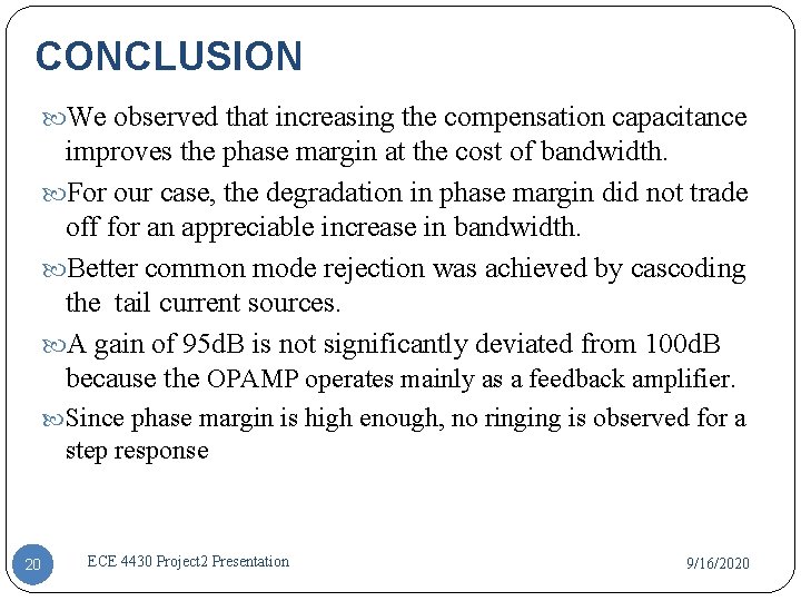
CONCLUSION We observed that increasing the compensation capacitance improves the phase margin at the cost of bandwidth. For our case, the degradation in phase margin did not trade off for an appreciable increase in bandwidth. Better common mode rejection was achieved by cascoding the tail current sources. A gain of 95 d. B is not significantly deviated from 100 d. B because the OPAMP operates mainly as a feedback amplifier. Since phase margin is high enough, no ringing is observed for a step response 20 ECE 4430 Project 2 Presentation 9/16/2020
Thank you… Questions? ? 21 ECE 4430 Project 2 Presentation 9/16/2020