HKN ECE 120 Midterm 3 Topic Overview Finite


")

![Details FETCH • • • MAR ← PC PC ← PC+1 MDR ← M[MAR]](https://slidetodoc.com/presentation_image/cd3957be46e8f2e47725676ec1954ec0/image-19.jpg "Details FETCH • • • MAR ← PC PC ← PC+1 MDR ← M[MAR]")


- Slides: 25
HKN ECE 120 Midterm 3
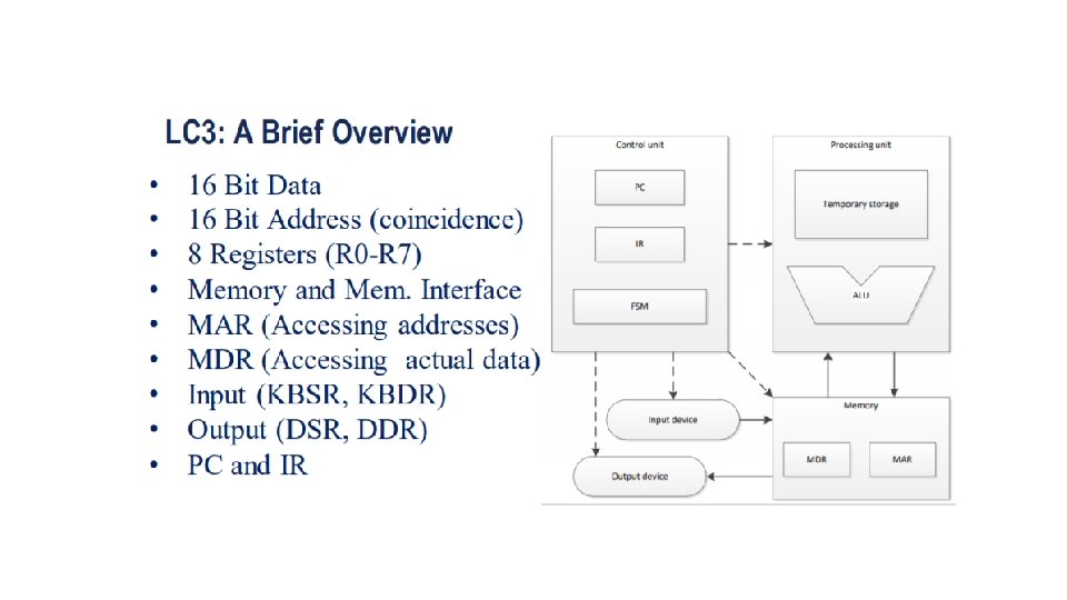
Topic Overview • Finite State Machine • Analysis, Design, Counter Design • Memory • Flip flops, RAM, Tri-state buffer • Addressability • How to construct from smaller blocks • LC 3 • • Von Neumann Architecture LC 3 Architecture ISA Instruction Cycle
S'-R' Latch • If S = R, then Q and P can't store a bit. • When S' is 0 and R' is 1, stores 1 into Q. • When S' is 1 and R' is 0, stores 0 into Q.
D latch • D stands for the DATA, WE stands for Write Enable • Stores the value of D when WE is high.
D Flip Flops • Made from two D latches • D latch behavior: C D R S Q+ Definition 1 0 0 Reset 1 1 0 1 1 Set 0 0 Q No change 0 1 1 No change • D flip flop stores the input bit D when clock goes low to high
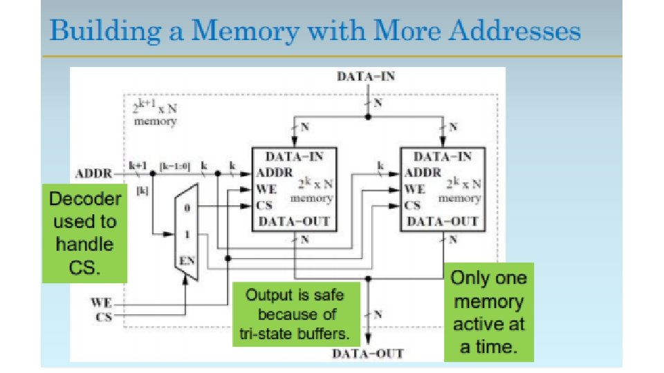
Bit Slice Design • Design 1 component for a single bit • Repeat it k times for a k-bit design Example of bit slice design: Ripple Carry Adder
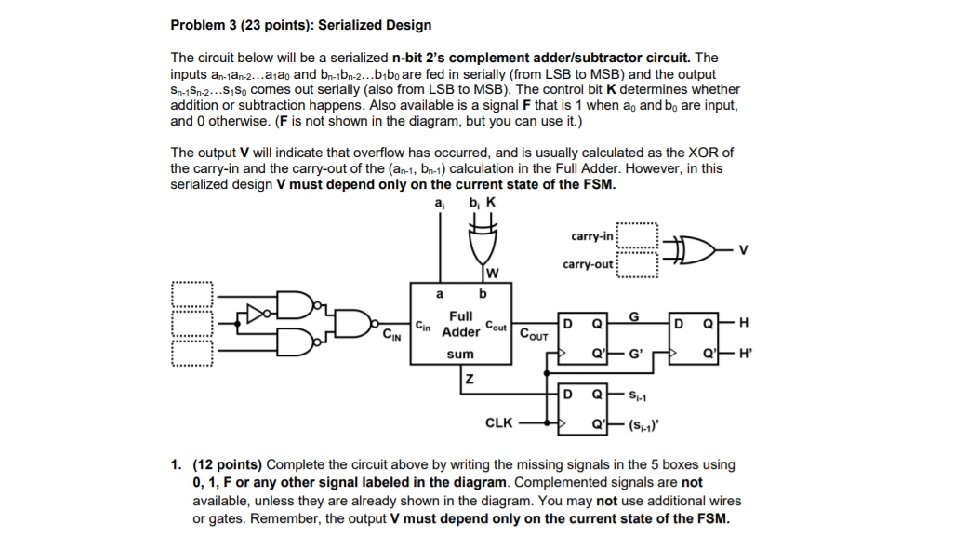
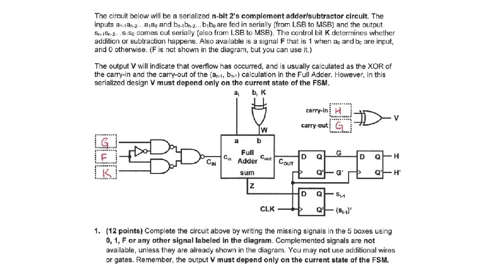
Serialized Design • Same as a bit slice design, except instead of many bit slices only use 1 • Use flip-flops to store intermediate results • Compute each bit slice in sequence, over time
Serialized Design • The ‘F’ Signal is 1 when the first bit of data enters, 0 otherwise • Use the ‘F’ signal to initialize your registers to the correct value • In the full adder example, this means load the register with carry in of 0
Bit Slice VS Serial • Area • For large number of bits, serial uses less area • For smaller number of bits, bit slice uses less area • Speed • Bit slice is usually faster • Serial is usually slower
Tri-State Buffers • When enable is 1, they act as a wire • When enable is 0, they act as high impedance (disconnected)
Finite State Machine 3 Main Components of FSMs: • Next state logic • Current state • Output logic How many bits are needed to represent N states in a standard FSM?
FSMs In Detail • 2 types: Mealy and Moore • Moore: Outputs are a function of current state only • Mealy: Outputs are a function of current state and inputs • Mealy machines use less states • 5 key elements: • • • Finite number of states Finite number of inputs Finite number of outputs Explicit number of state transitions Explicit definition of outputs as a function of state (and as function of inputs for Mealy machines)
FSM Design 1. List all inputs to your FSM 2. List all outputs from the FSM 3. Create a truth table for the FSM a) State and inputs on the left b) Next state and outputs on the right c) Outputs should be the same for the same current state (unless Mealy machine) 4. Create a state diagram 5. K-maps, etc.
EVERY 16 BIT INSTRUCTION CORRESPONDS TO ONE OF THESE! CHEAT SHEET IS YOUR SAVIOR HERE! Side: Don't worry about JSR, JSRR, TRAP, or RTI yet, just know they exist
How to read your Cheat Sheet (for ISA)
Instruction Cycle!
Details FETCH • • • MAR ← PC PC ← PC+1 MDR ← M[MAR] IR ← MDR Used to obtain the next instruction IMPORTANT! PC is incremented to next spot BEFORE current instruction put in IR DECODE - Opcode (IR[15: 12]) examined (first 4 bits)