ECE 120 Midterm 2 HKN Review Session Overview




- Slides: 38

ECE 120 Midterm 2 HKN Review Session

Overview of Review ● CMOS logic, Boolean expressions, Boolean Algebra ● K-maps, SOP, POS ● 2 -level networks ● Adders, ALUs, and Bit Slice Design ● Multiplexers, Decoders ● Flip-Flops and Latches (S-R & D) ● FSM Design, Moore Machines ● Practice Exams! (The not so secret sauce in success)

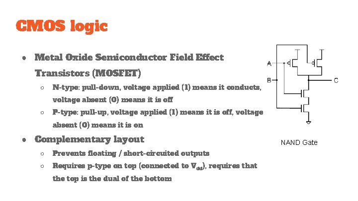
CMOS logic ● Metal Oxide Semiconductor Field Effect Transistors (MOSFET) ○ N-type: pull-down, voltage applied (1) means it conducts, voltage absent (0) means it is off ○ P-type: pull-up, voltage applied (1) means it is off, voltage absent (0) means it is on ● Complementary layout ○ Prevents floating / short-circuited outputs ○ Requires p-type on top (connected to Vdd), requires that the top is the dual of the bottom NAND Gate

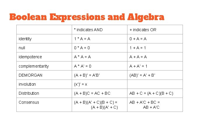
Boolean Expressions and Algebra * indicates AND + indicates OR identity 1*A=A 0+A=A null 0*A=0 1+A=1 idempotence A*A=A A+A=A complementarity A * A’ = 0 A + A’ = 1 DEMORGAN (A + B)’ = A’B’ (AB)’ = A’ + B’ involution (x’)’ = x Distribution (A + B)C = AC + BC AB + C = (A + C)(B + C) Consensus (A + B)(A’ + C)(B + C) = (A + B)(A’ + C) AB + A’C + BC = AB + A’C

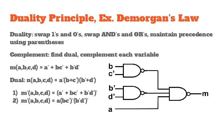
Duality Principle, Ex. Demorgan’s Law Duality: swap 1’s and 0’s, swap AND’s and OR’s, maintain precedence using parentheses Complement: find dual, complement each variable m(a, b, c, d) = a’ + bc’ + b’d’ Dual: n(a, b, c, d) = a’(b+c’)(b’+d’) 1) m’(a, b, c, d) = (a’ + bc’ + b’d’)’ 2) m’(a, b, c, d) = a(bc’)’(b’d’)’

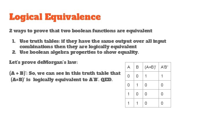
Logical Equivalence 2 ways to prove that two boolean functions are equivalent 1. Use truth tables: if they have the same output over all input combinations then they are logically equivalent 2. Use boolean algebra properties to show equality. Let’s prove de. Morgan’s law: (A + B)’: So, we can see in this truth table that (A+B)’ is logically equivalent to A’B’. QED. A B (A+B)’ A’B’ 0 0 1 1 0 0 0 1 1 0 0

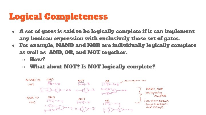
Logical Completeness ● A set of gates is said to be logically complete if it can implement any boolean expression with exclusively those set of gates. ● For example, NAND and NOR are individually logically complete as well as AND, OR, and NOT together. ○ How? ○ What about NOT? Is NOT logically complete?

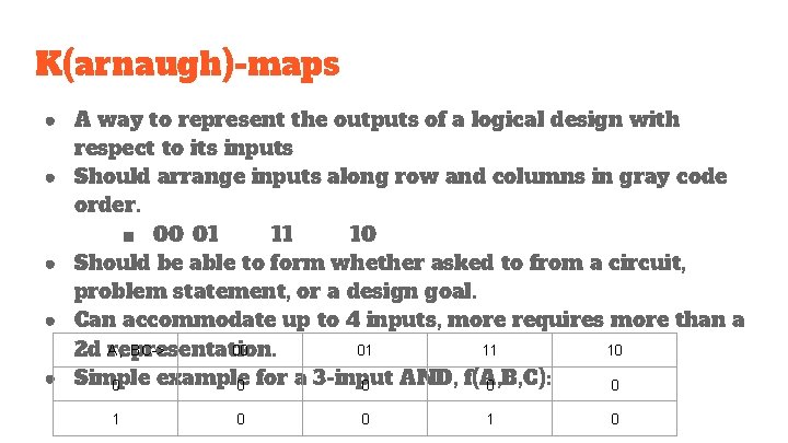
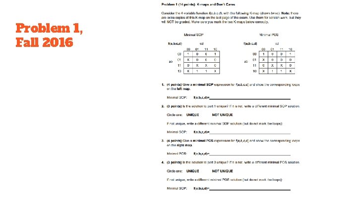
K(arnaugh)-maps ● A way to represent the outputs of a logical design with respect to its inputs ● Should arrange inputs along row and columns in gray code order. ■ 00 01 11 10 ● Should be able to form whether asked to from a circuit, problem statement, or a design goal. ● Can accommodate up to 4 inputs, more requires more than a A, BC-> 00 01 11 10 2 d representation. ● Simple example AND, f(A, B, C): 0 0 for a 3 -input 0 0 0 1 0

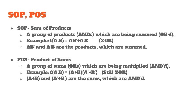
SOP, POS ● SOP- Sum of Products ○ A group of products (ANDs) which are being summed (OR’d). ○ Example: f(A, B) = AB’+A’B (XOR) ○ AB’ and A’B are the products, which are summed. ● POS- Product of Sums ○ A group of sums (ORs) which are being multiplied (AND’d). ○ Example: f(A, B) = (A+B)(A’+B’) (Still XOR) ○ (A+B) and (A’+B’) are the sums, which are AND’d.

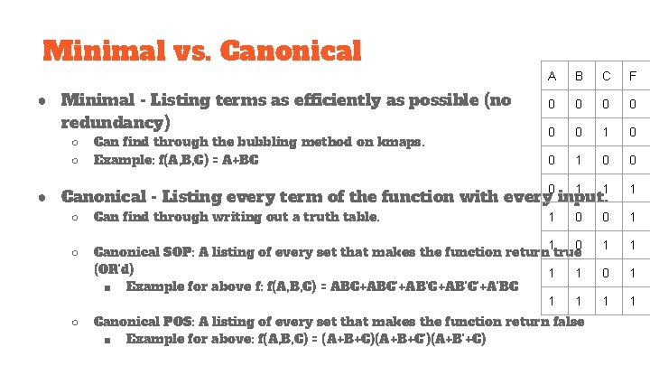
Minimal vs. Canonical A B C F 0 0 0 1 1 0 0 1 1 0 Canonical SOP: A listing of every set that makes the function return true (OR’d) 1 1 ■ Example for above f: f(A, B, C) = ABC+ABC’+AB’C’+A’BC 1 1 0 1 1 1 ● Minimal - Listing terms as efficiently as possible (no redundancy) ○ ○ Can find through the bubbling method on kmaps. Example: f(A, B, C) = A+BC ● Canonical - Listing every term of the function with every input. ○ ○ ○ Can find through writing out a truth table. Canonical POS: A listing of every set that makes the function return false ■ Example for above: f(A, B, C) = (A+B+C)(A+B+C’)(A+B’+C)

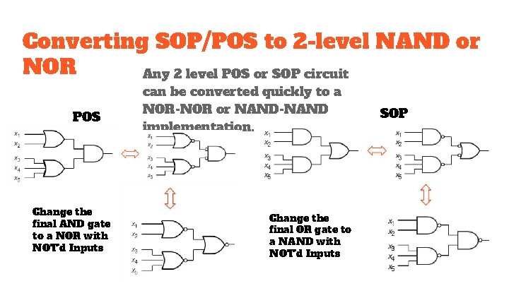
Converting SOP/POS to 2 -level NAND or NOR Any 2 level POS or SOP circuit POS Change the final AND gate to a NOR with NOT’d Inputs can be converted quickly to a NOR-NOR or NAND-NAND implementation. Change the final OR gate to a NAND with NOT’d Inputs SOP

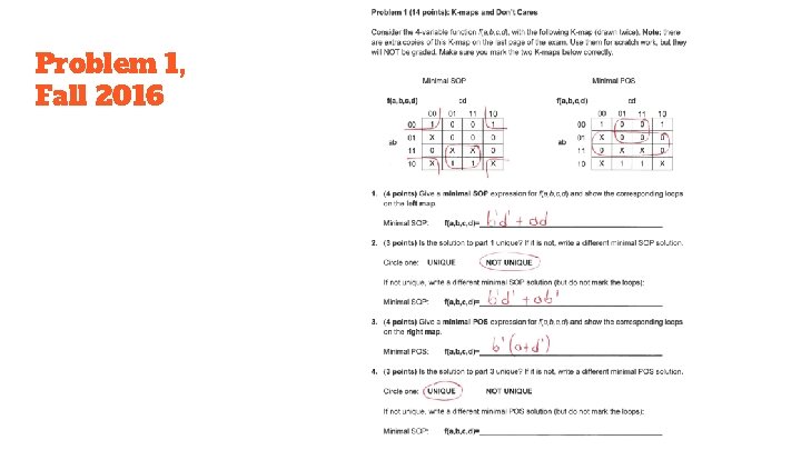
Optimized Boolean Expressions ● When trying to find the Boolean expression for the outputs of a function ○ ○ consider both the POS and SOP forms Check which of these minimises the total number of gates ○ The largest grouping of 1’s not fully contained by another grouping of 1’s (with power of 2 dimensions, ie. 2, 4, 8) ● Prime implicants ● Uniqueness ○ ○ Look for other prime implicants of equal size that are not currently being used in your minimal expression If you can write another function with the same number of terms, then it is not unique ● Don’t Cares ○ ○ Symbol: X, used if the output can be a 0 or a 1 Can be included in any kmap circling

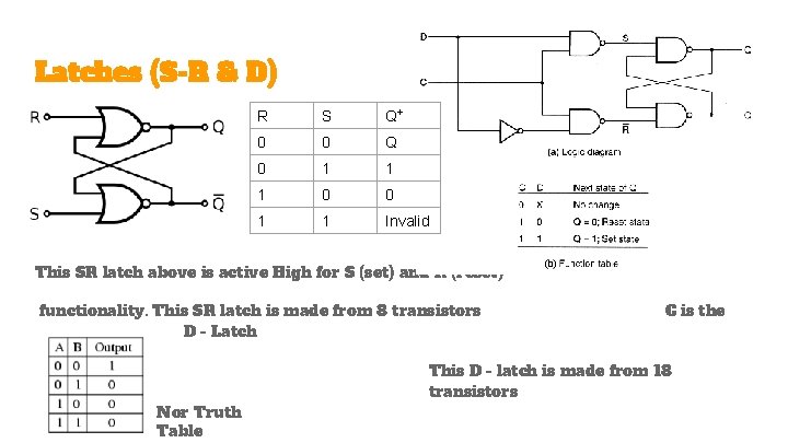
Latches (S-R & D) R S Q+ 0 0 Q 0 1 1 1 0 0 1 1 Invalid This SR latch above is active High for S (set) and R (reset) functionality. This SR latch is made from 8 transistors enable bit for this D - Latch Nor Truth Table C is the This D - latch is made from 18 transistors

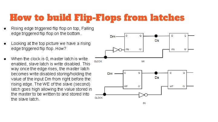
How to build Flip-Flops from latches ● Rising edge triggered flip flop on top, Falling edge triggered flip flop on the bottom. ● Looking at the top picture we have a rising edge triggered flip flop. How? ● When the clock is 0, master latch is write enabled, slave latch is write disabled. This way once the edge rises, the master latch becomes write disabled storing/holding the value of the input Dm from right before the rising edge. The WE of the slave (second) latch goes high allowing the value stored in the master to be written to and stored into the slave latch.

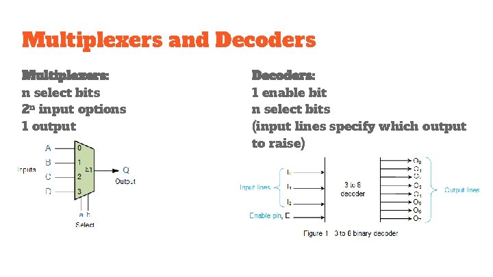
Multiplexers and Decoders Multiplexers: n select bits 2 n input options 1 output Decoders: 1 enable bit n select bits (input lines specify which output to raise) 2 n possible outputs (one high at a time)

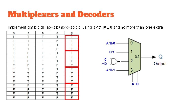
Multiplexers and Decoders Implement g(a, b, c, d)=ab+a’b+ab’c’d’ using a 4: 1 MUX and no more than one extra gate. A/B/0 B/1 C ~D A/B/1 A B

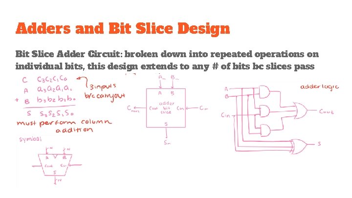
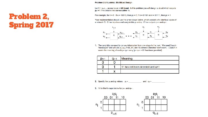
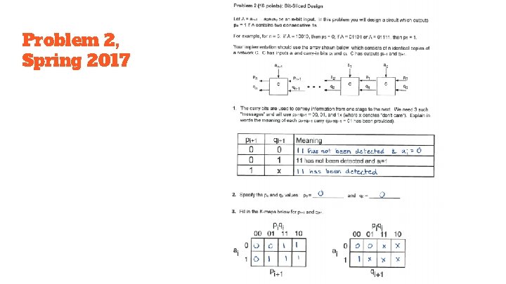
Adders and Bit Slice Design Bit Slice Adder Circuit: broken down into repeated operations on individual bits, this design extends to any # of bits bc slices pass information between them

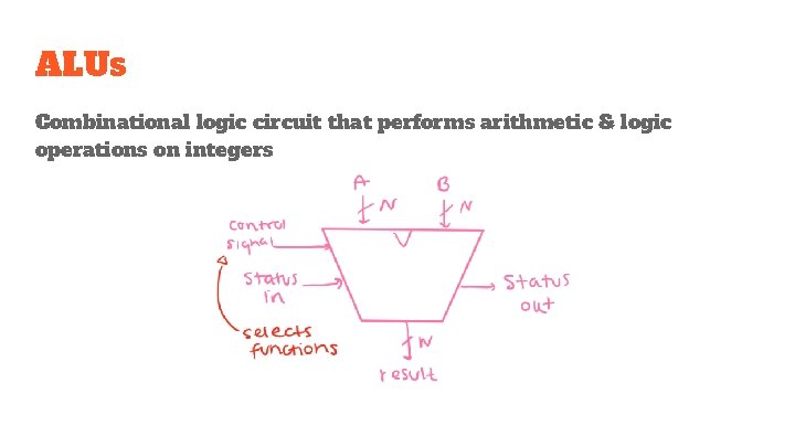
ALUs Combinational logic circuit that performs arithmetic & logic operations on integers

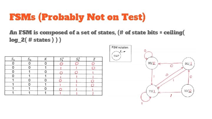
FSMs (Probably Not on Test) An FSM is composed of a set of states, (# of state bits = ceiling( log_2( # states ) ) )

Practice Questions

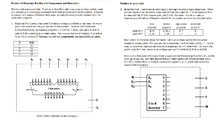
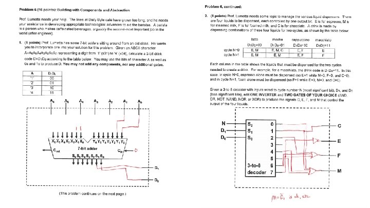
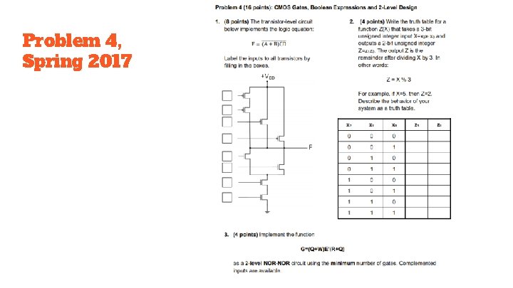
Problem 4, Spring 2017

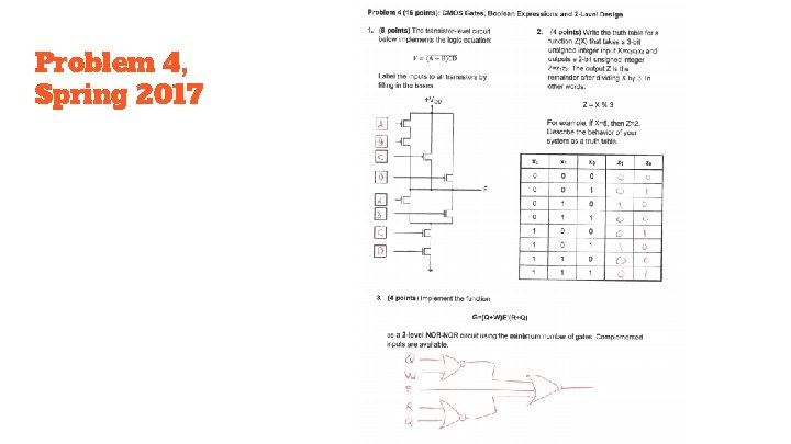
Problem 4, Spring 2017

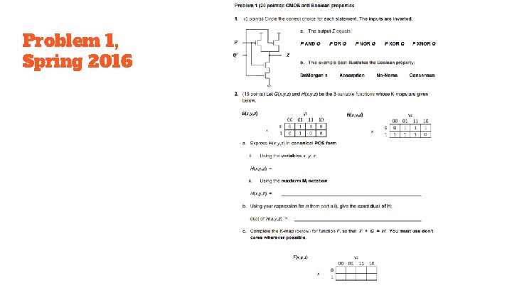
Problem 1, Spring 2016

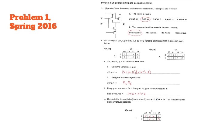
Problem 1, Spring 2016

Problem 2, Spring 2017

Problem 2, Spring 2017

Problem 1, Fall 2016

Problem 1, Fall 2016

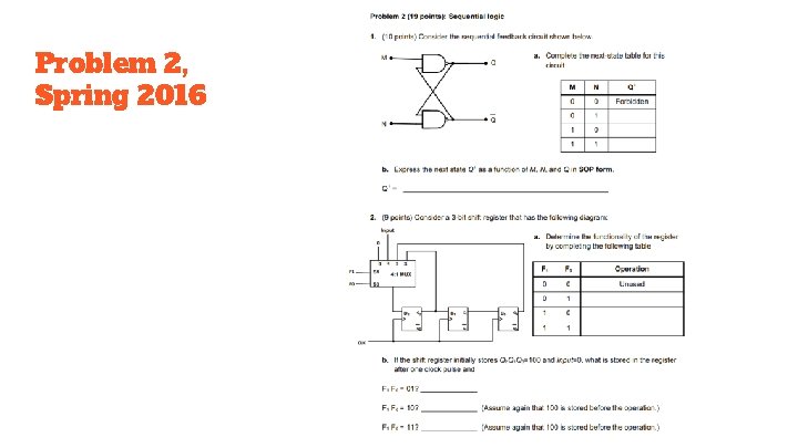
Problem 2, Spring 2016

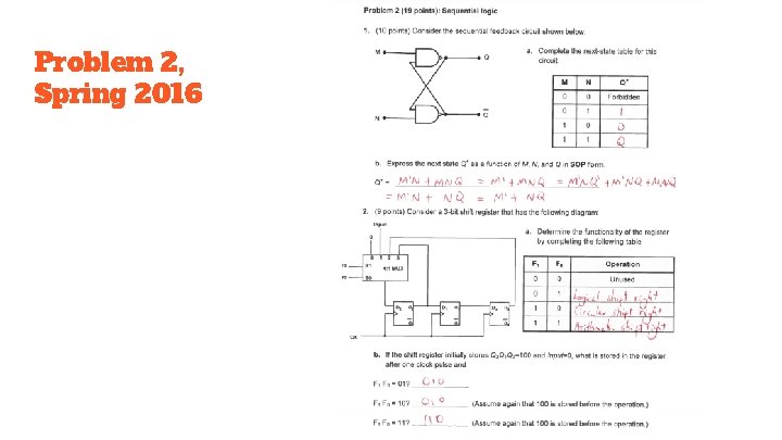
Problem 2, Spring 2016

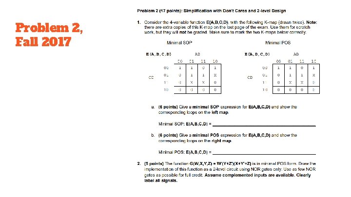
Problem 2, Fall 2017

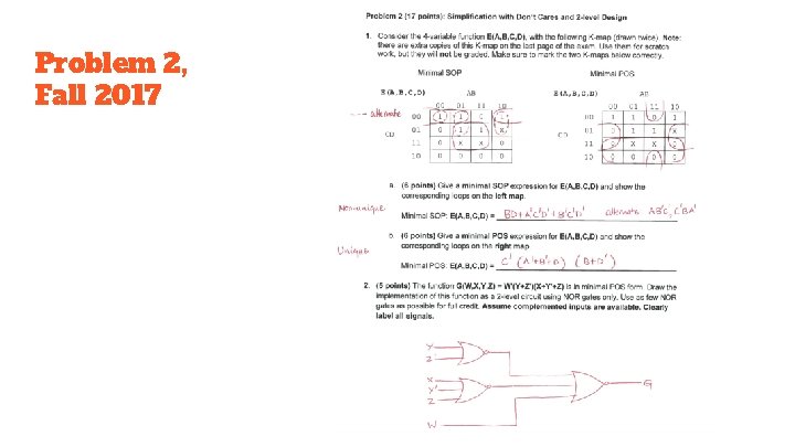
Problem 2, Fall 2017

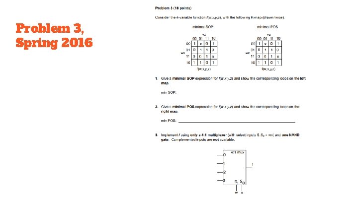
Problem 3, Spring 2016

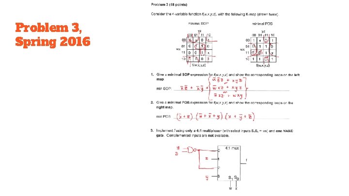
Problem 3, Spring 2016

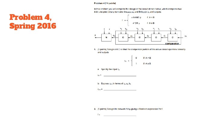
Problem 4, Spring 2016

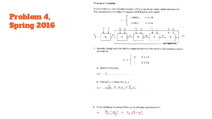
Problem 4, Spring 2016
