CS 150 Midterm 2 Review Joy Another midterm
![Review of FSM Timing decode fetch step 1 step 2 IR mem[PC]; PC + Review of FSM Timing decode fetch step 1 step 2 IR mem[PC]; PC +](https://slidetodoc.com/presentation_image_h/8cbe0f008d5c687ce56224042028dfe6/image-185.jpg)
- Slides: 191

CS 150 Midterm 2 Review Joy! Another midterm

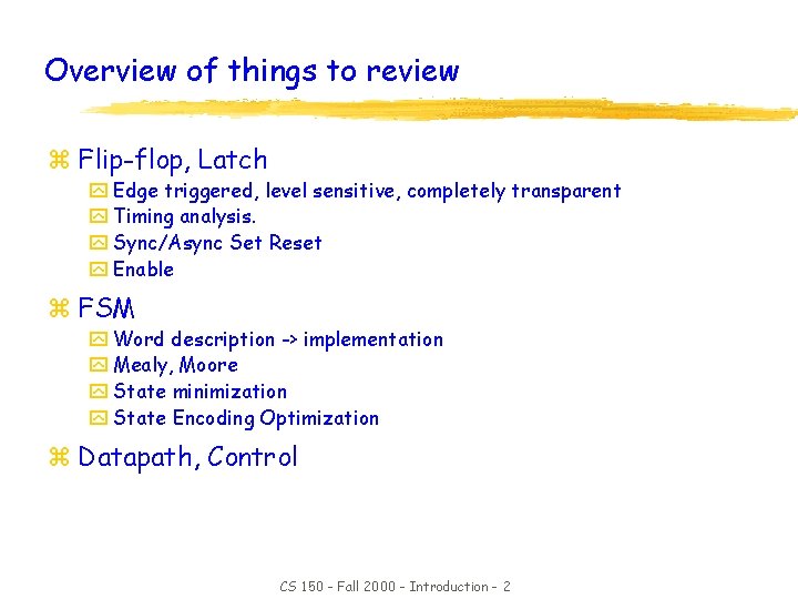
Overview of things to review z Flip-flop, Latch y Edge triggered, level sensitive, completely transparent y Timing analysis. y Sync/Async Set Reset y Enable z FSM y Word description -> implementation y Mealy, Moore y State minimization y State Encoding Optimization z Datapath, Control CS 150 - Fall 2000 - Introduction - 2

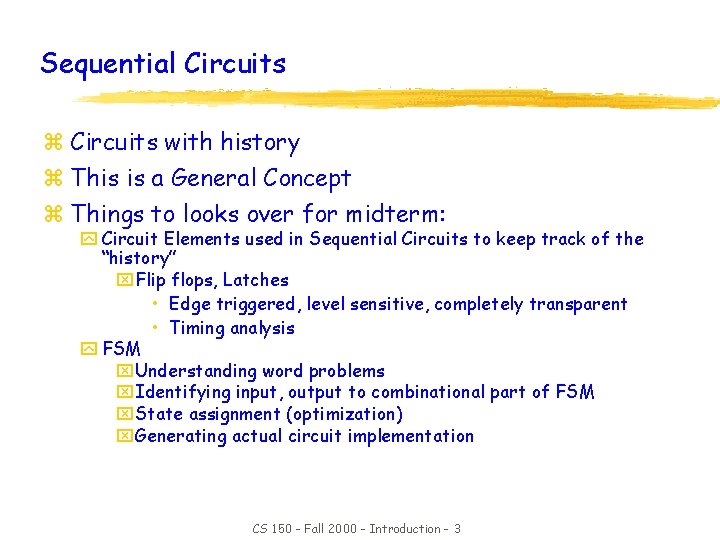
Sequential Circuits z Circuits with history z This is a General Concept z Things to looks over for midterm: y Circuit Elements used in Sequential Circuits to keep track of the “history” x. Flip flops, Latches • Edge triggered, level sensitive, completely transparent • Timing analysis y FSM x. Understanding word problems x. Identifying input, output to combinational part of FSM x. State assignment (optimization) x. Generating actual circuit implementation CS 150 - Fall 2000 - Introduction - 3

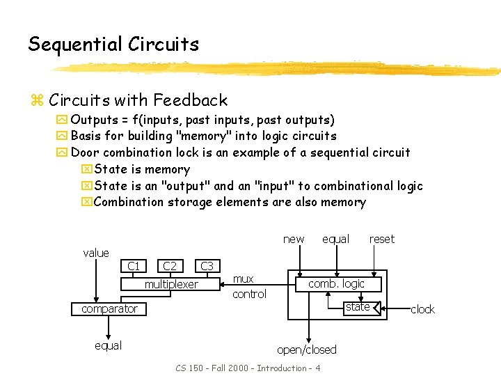
Sequential Circuits z Circuits with Feedback y Outputs = f(inputs, past outputs) y Basis for building "memory" into logic circuits y Door combination lock is an example of a sequential circuit x. State is memory x. State is an "output" and an "input" to combinational logic x. Combination storage elements are also memory new equal reset value C 1 C 2 multiplexer C 3 mux control comb. logic state comparator equal open/closed CS 150 - Fall 2000 - Introduction - 4 clock

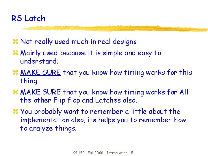
RS Latch z Not really used much in real designs z Mainly used because it is simple and easy to understand. z MAKE SURE that you know how timing works for this thing z MAKE SURE that you know how timing works for All the other Flip flop and Latches also. z You probably want to remember a little about the implementation also, its helps you to remember how to analyze things. CS 150 - Fall 2000 - Introduction - 5

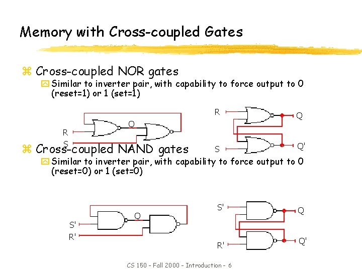
Memory with Cross-coupled Gates z Cross-coupled NOR gates y Similar to inverter pair, with capability to force output to 0 (reset=1) or 1 (set=1) R Q S Q' Q R S z Cross-coupled NAND gates y Similar to inverter pair, with capability to force output to 0 (reset=0) or 1 (set=0) S' R' Q S' R' CS 150 - Fall 2000 - Introduction - 6 Q Q'

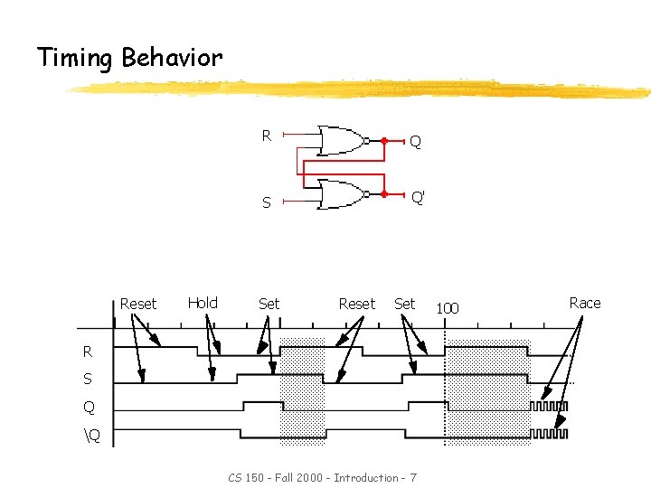
Timing Behavior Reset Hold R Q S Q' Set Reset Set R S Q Q CS 150 - Fall 2000 - Introduction - 7 100 Race

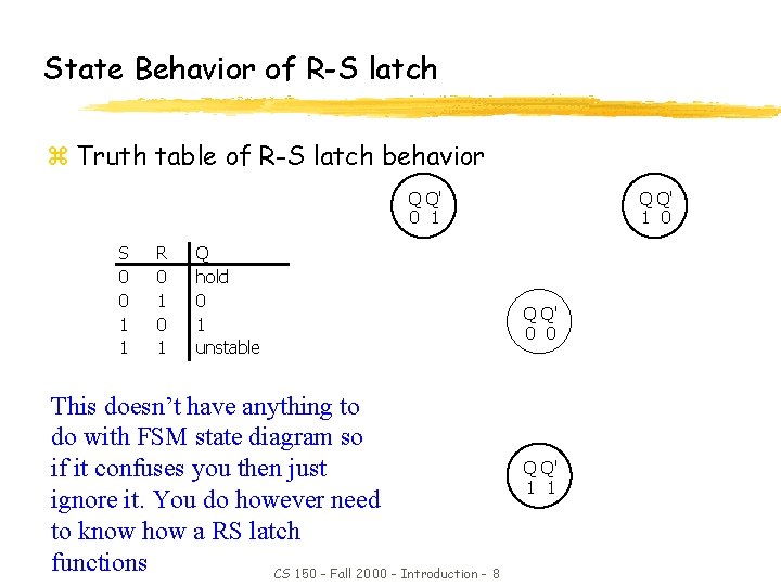
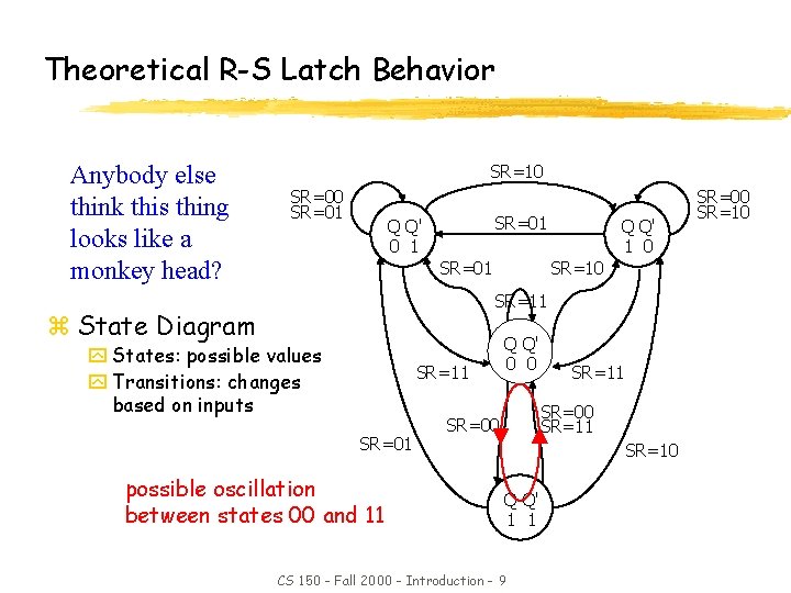
State Behavior of R-S latch z Truth table of R-S latch behavior Q Q' 0 1 S 0 0 1 1 R 0 1 Q hold 0 1 unstable This doesn’t have anything to do with FSM state diagram so if it confuses you then just ignore it. You do however need to know how a RS latch functions CS 150 - Fall 2000 - Introduction - 8 Q Q' 1 0 Q Q' 0 0 Q Q' 1 1

Theoretical R-S Latch Behavior Anybody else think this thing looks like a monkey head? SR=10 SR=01 Q Q' 0 1 SR=01 Q Q' 1 0 SR=11 z State Diagram y States: possible values y Transitions: changes based on inputs SR=11 SR=01 possible oscillation between states 00 and 11 Q Q' 0 0 SR=11 SR=00 SR=10 Q Q' 1 1 CS 150 - Fall 2000 - Introduction - 9 SR=00 SR=10

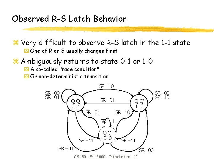
Observed R-S Latch Behavior z Very difficult to observe R-S latch in the 1 -1 state y One of R or S usually changes first z Ambiguously returns to state 0 -1 or 1 -0 y A so-called "race condition" y Or non-deterministic transition SR=10 SR=01 Q Q' 0 1 SR=01 Q Q' 1 0 SR=11 Q Q' 0 0 SR=11 SR=00 CS 150 - Fall 2000 - Introduction - 10 SR=00 SR=10

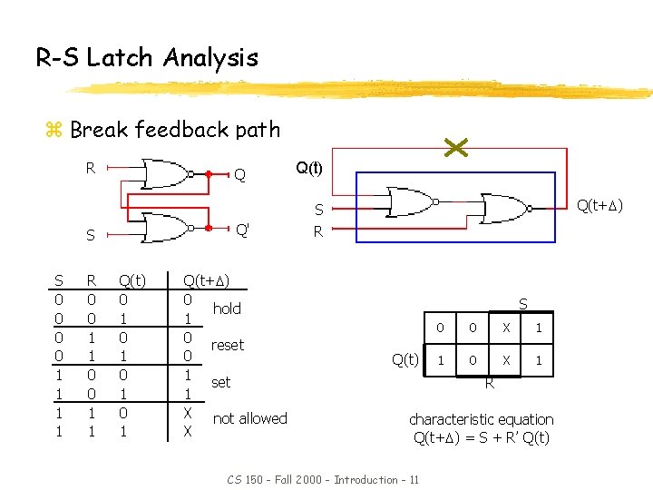
R-S Latch Analysis z Break feedback path R Q Q' S S 0 0 1 1 R 0 0 1 1 Q(t) 0 1 0 1 Q(t+ ) 0 hold 1 0 reset 0 1 set 1 X not allowed X Q(t) Q(t+ ) S R S Q(t) 0 0 X 1 1 0 X 1 R characteristic equation Q(t+ ) = S + R’ Q(t) CS 150 - Fall 2000 - Introduction - 11

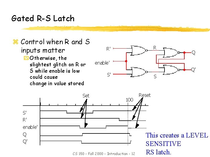
Gated R-S Latch z Control when R and S inputs matter y Otherwise, the slightest glitch on R or S while enable is low could cause change in value stored Set R R' Q enable' Q' S' S 100 Reset S' R' enable' Q Q' CS 150 - Fall 2000 - Introduction - 12 This creates a LEVEL SENSITIVE RS latch.

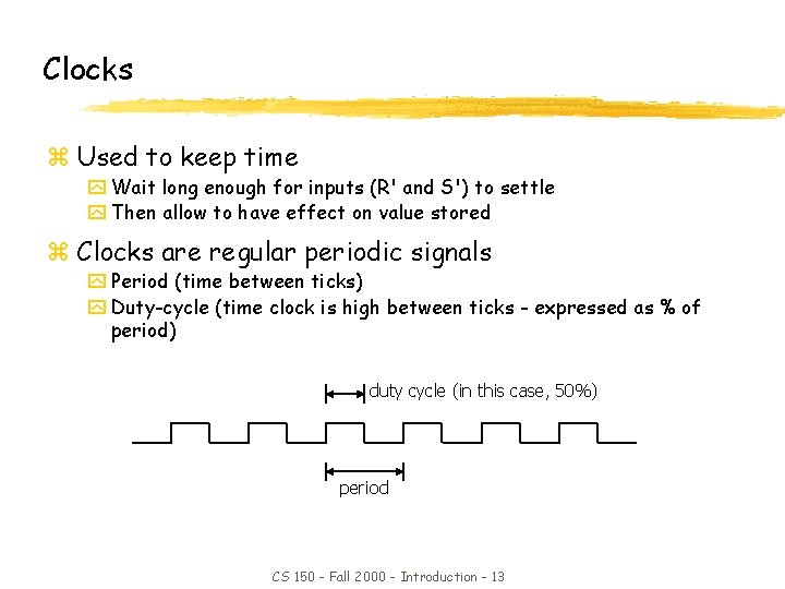
Clocks z Used to keep time y Wait long enough for inputs (R' and S') to settle y Then allow to have effect on value stored z Clocks are regular periodic signals y Period (time between ticks) y Duty-cycle (time clock is high between ticks - expressed as % of period) duty cycle (in this case, 50%) period CS 150 - Fall 2000 - Introduction - 13

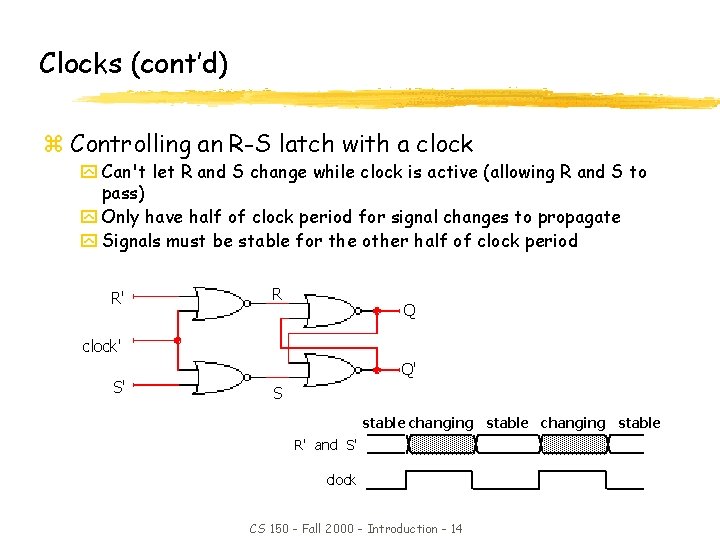
Clocks (cont’d) z Controlling an R-S latch with a clock y Can't let R and S change while clock is active (allowing R and S to pass) y Only have half of clock period for signal changes to propagate y Signals must be stable for the other half of clock period R' R Q clock' S' Q' S stable changing stable R' and S' clock CS 150 - Fall 2000 - Introduction - 14

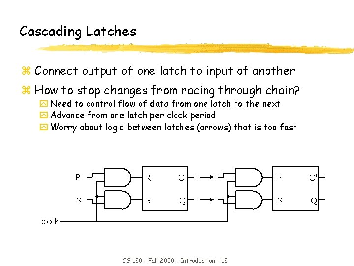
Cascading Latches z Connect output of one latch to input of another z How to stop changes from racing through chain? y Need to control flow of data from one latch to the next y Advance from one latch per clock period y Worry about logic between latches (arrows) that is too fast R R Q' S S Q clock CS 150 - Fall 2000 - Introduction - 15

Master-Slave RS (flip flop? ? ) z Another Thing you need to stuff in your brain for this test z Again make sure you know the timing for this sucker z Also don’t for get the 1’s catching problem, professor Katz seems to like this one. CS 150 - Fall 2000 - Introduction - 16

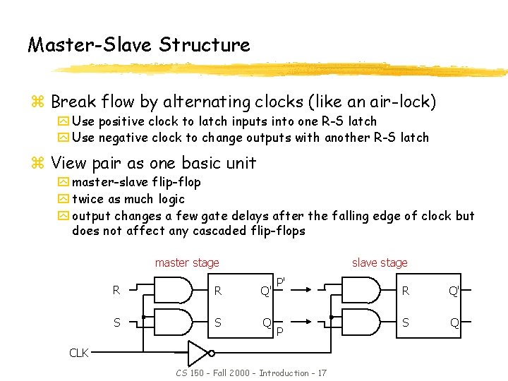
Master-Slave Structure z Break flow by alternating clocks (like an air-lock) y Use positive clock to latch inputs into one R-S latch y Use negative clock to change outputs with another R-S latch z View pair as one basic unit y master-slave flip-flop y twice as much logic y output changes a few gate delays after the falling edge of clock but does not affect any cascaded flip-flops slave stage master stage R R Q' S S Q P' P CLK CS 150 - Fall 2000 - Introduction - 17 R Q' S Q

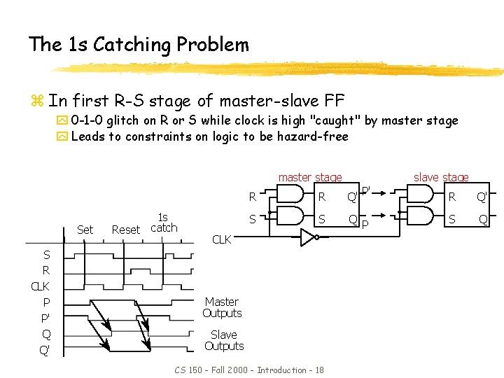
The 1 s Catching Problem z In first R-S stage of master-slave FF y 0 -1 -0 glitch on R or S while clock is high "caught" by master stage y Leads to constraints on logic to be hazard-free slave stage master stage Set S R CLK P P' Q Q' 1 s Reset catch R R Q' S S Q CLK Master Outputs Slave Outputs CS 150 - Fall 2000 - Introduction - 18 P' P R Q' S Q

D Flip-Flops (Ah something that people actually use for a change) z This is the bread and butter of Logic Design so MAKE SURE you know EDGE TRIGGERED flip flops like the back of your hand. z (fortunately they are very easy to understand functionally which is why people like to use them) CS 150 - Fall 2000 - Introduction - 19

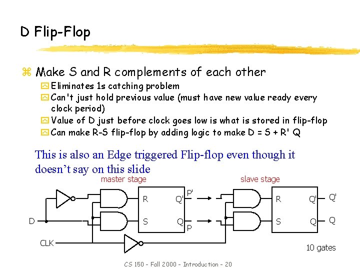
D Flip-Flop z Make S and R complements of each other y Eliminates 1 s catching problem y Can't just hold previous value (must have new value ready every clock period) y Value of D just before clock goes low is what is stored in flip-flop y Can make R-S flip-flop by adding logic to make D = S + R' Q This is also an Edge triggered Flip-flop even though it doesn’t say on this slide slave stage master stage D R Q' S Q P' P CLK R Q' Q' S Q Q 10 gates CS 150 - Fall 2000 - Introduction - 20

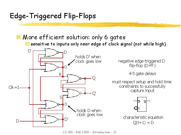
Edge-Triggered Flip-Flops z More efficient solution: only 6 gates y sensitive to inputs only near edge of clock signal (not while high) D’ D holds D' when clock goes low negative edge-triggered D flip-flop (D-FF) 0 R Q Clk=1 Q’ S 4 -5 gate delays must respect setup and hold time constraints to successfully capture input 0 D D’ holds D when clock goes low CS 150 - Fall 2000 - Introduction - 21 characteristic equation Q(t+1) = D

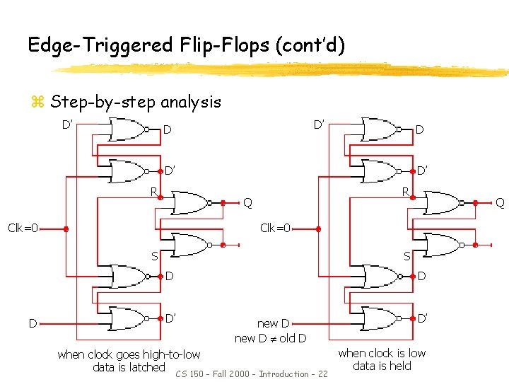
Edge-Triggered Flip-Flops (cont’d) z Step-by-step analysis D’ D’ D D D’ D’ R R Q Clk=0 S S D D Q D D’ new D old D when clock goes high-to-low data is latched CS 150 - Fall 2000 - Introduction - 22 D’ when clock is low data is held

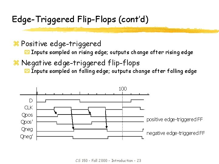
Edge-Triggered Flip-Flops (cont’d) z Positive edge-triggered y Inputs sampled on rising edge; outputs change after rising edge z Negative edge-triggered flip-flops y Inputs sampled on falling edge; outputs change after falling edge 100 D CLK Qpos' Qneg' positive edge-triggered FF negative edge-triggered FF CS 150 - Fall 2000 - Introduction - 23

Timing z Make sure you know how to analyze on a Clock cycle by clock cycle bases first z Setup and hold times are really just a general concept that you don’t need to know in deep detail. y Pretty important although probably much more important in EE 141 CS 150 - Fall 2000 - Introduction - 24

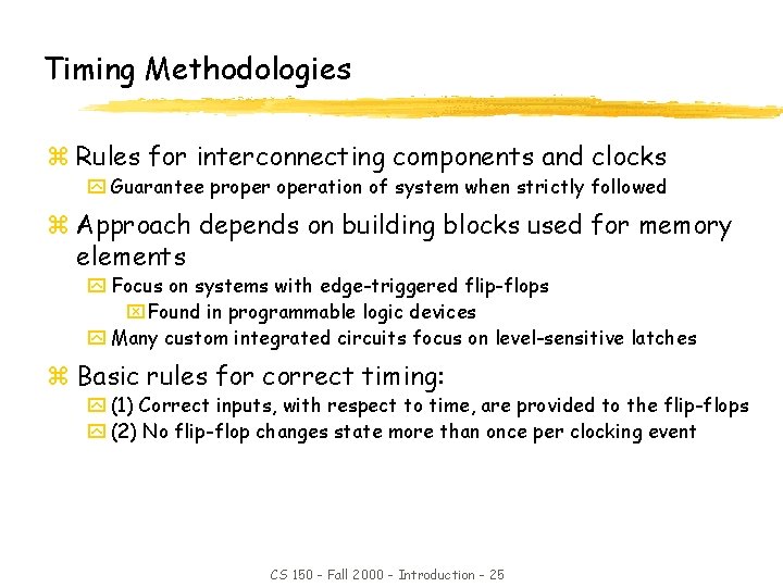
Timing Methodologies z Rules for interconnecting components and clocks y Guarantee properation of system when strictly followed z Approach depends on building blocks used for memory elements y Focus on systems with edge-triggered flip-flops x. Found in programmable logic devices y Many custom integrated circuits focus on level-sensitive latches z Basic rules for correct timing: y (1) Correct inputs, with respect to time, are provided to the flip-flops y (2) No flip-flop changes state more than once per clocking event CS 150 - Fall 2000 - Introduction - 25

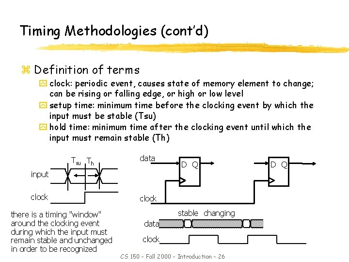
Timing Methodologies (cont’d) z Definition of terms y clock: periodic event, causes state of memory element to change; can be rising or falling edge, or high or low level y setup time: minimum time before the clocking event by which the input must be stable (Tsu) y hold time: minimum time after the clocking event until which the input must remain stable (Th) Tsu Th data D Q input clock there is a timing "window" around the clocking event during which the input must remain stable and unchanged in order to be recognized clock stable changing data clock CS 150 - Fall 2000 - Introduction - 26 D Q

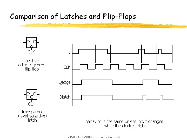
Comparison of Latches and Flip-Flops D Q CLK positive edge-triggered flip-flop D CLK Qedge D Q G Qlatch CLK transparent (level-sensitive) latch behavior is the same unless input changes while the clock is high CS 150 - Fall 2000 - Introduction - 27

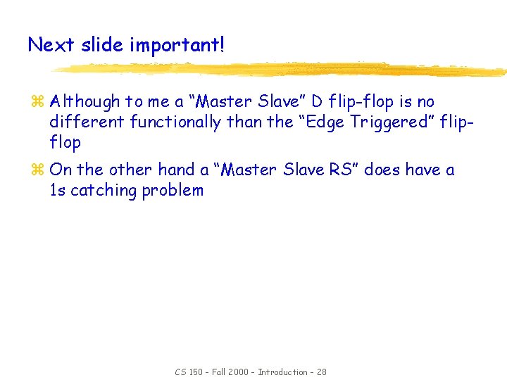
Next slide important! z Although to me a “Master Slave” D flip-flop is no different functionally than the “Edge Triggered” flipflop z On the other hand a “Master Slave RS” does have a 1 s catching problem CS 150 - Fall 2000 - Introduction - 28

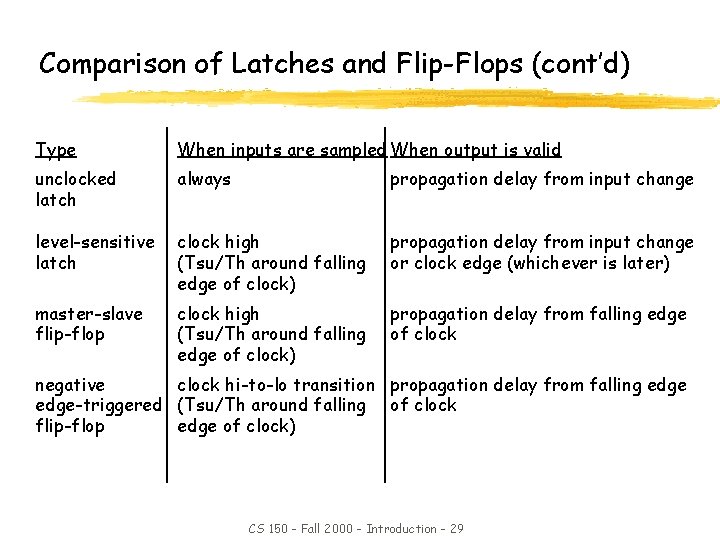
Comparison of Latches and Flip-Flops (cont’d) Type When inputs are sampled When output is valid unclocked latch always propagation delay from input change level-sensitive latch clock high (Tsu/Th around falling edge of clock) propagation delay from input change or clock edge (whichever is later) master-slave flip-flop clock high (Tsu/Th around falling edge of clock) propagation delay from falling edge of clock negative clock hi-to-lo transition propagation delay from falling edge-triggered (Tsu/Th around falling of clock flip-flop edge of clock) CS 150 - Fall 2000 - Introduction - 29

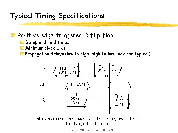
Typical Timing Specifications z Positive edge-triggered D flip-flop y Setup and hold times y Minimum clock width y Propagation delays (low to high, high to low, max and typical) D CLK Q Tsu Th 20 ns 5 ns Tsu 20 ns Th 5 ns Tw 25 ns Tplh 25 ns 13 ns Tphl 40 ns 25 ns all measurements are made from the clocking event that is, the rising edge of the clock CS 150 - Fall 2000 - Introduction - 30

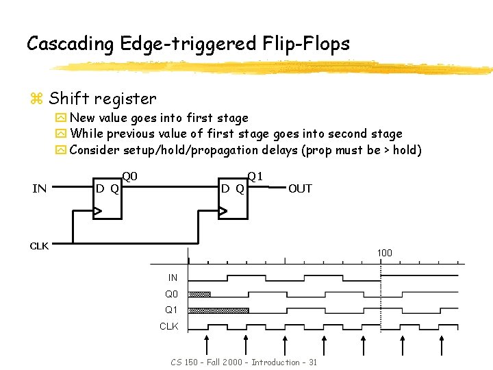
Cascading Edge-triggered Flip-Flops z Shift register y New value goes into first stage y While previous value of first stage goes into second stage y Consider setup/hold/propagation delays (prop must be > hold) IN D Q Q 0 D Q Q 1 OUT CLK 100 IN Q 0 Q 1 CLK CS 150 - Fall 2000 - Introduction - 31

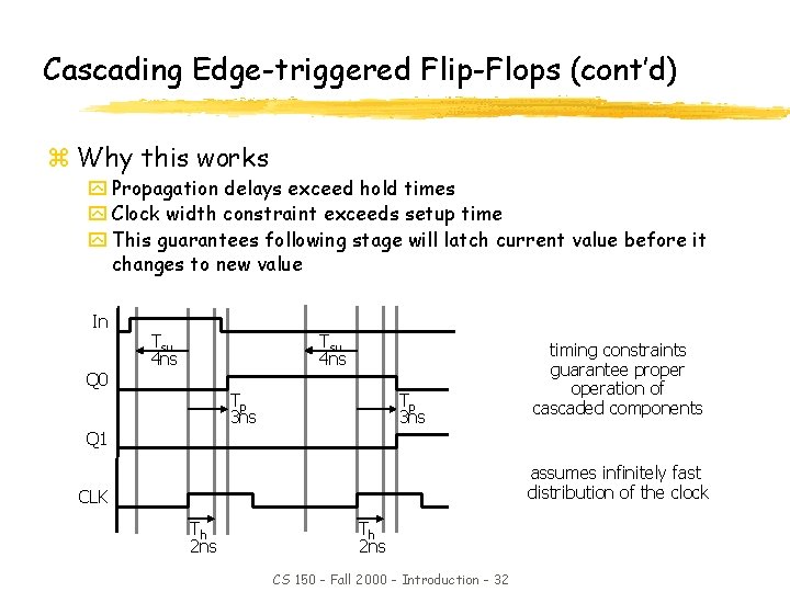
Cascading Edge-triggered Flip-Flops (cont’d) z Why this works y Propagation delays exceed hold times y Clock width constraint exceeds setup time y This guarantees following stage will latch current value before it changes to new value In Tsu 4 ns Q 0 Tp 3 ns timing constraints guarantee properation of cascaded components Q 1 assumes infinitely fast distribution of the clock CLK Th 2 ns CS 150 - Fall 2000 - Introduction - 32

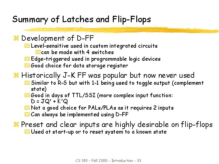
Summary of Latches and Flip-Flops z Development of D-FF y Level-sensitive used in custom integrated circuits xcan be made with 4 switches y Edge-triggered used in programmable logic devices y Good choice for data storage register z Historically J-K FF was popular but now never used y Similar to R-S but with 1 -1 being used to toggle output (complement state) y Good in days of TTL/SSI (more complex input function: D = JQ' + K'Q y Not a good choice for PALs/PLAs as it requires 2 inputs y Can always be implemented using D-FF z Preset and clear inputs are highly desirable on flip-flops y Used at start-up or to reset system to a known state CS 150 - Fall 2000 - Introduction - 33

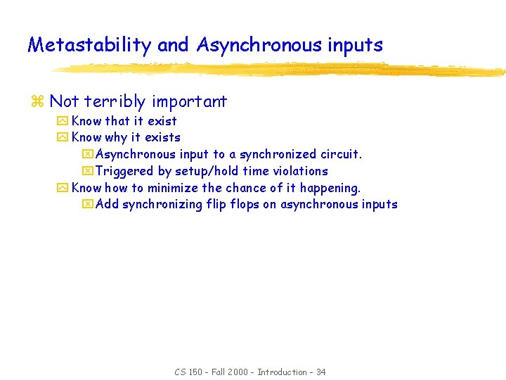
Metastability and Asynchronous inputs z Not terribly important y Know that it exist y Know why it exists x. Asynchronous input to a synchronized circuit. x. Triggered by setup/hold time violations y Know how to minimize the chance of it happening. x. Add synchronizing flip flops on asynchronous inputs CS 150 - Fall 2000 - Introduction - 34

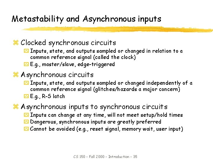
Metastability and Asynchronous inputs z Clocked synchronous circuits y Inputs, state, and outputs sampled or changed in relation to a common reference signal (called the clock) y E. g. , master/slave, edge-triggered z Asynchronous circuits y Inputs, state, and outputs sampled or changed independently of a common reference signal (glitches/hazards a major concern) y E. g. , R-S latch z Asynchronous inputs to synchronous circuits y Inputs can change at any time, will not meet setup/hold times y Dangerous, synchronous inputs are greatly preferred y Cannot be avoided (e. g. , reset signal, memory wait, user input) CS 150 - Fall 2000 - Introduction - 35

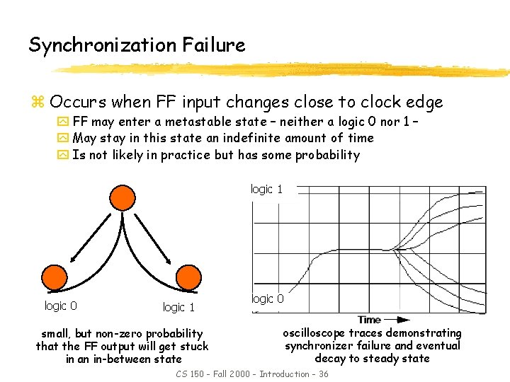
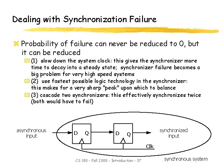
Synchronization Failure z Occurs when FF input changes close to clock edge y FF may enter a metastable state – neither a logic 0 nor 1 – y May stay in this state an indefinite amount of time y Is not likely in practice but has some probability logic 1 logic 0 logic 1 small, but non-zero probability that the FF output will get stuck in an in-between state logic 0 oscilloscope traces demonstrating synchronizer failure and eventual decay to steady state CS 150 - Fall 2000 - Introduction - 36

Dealing with Synchronization Failure z Probability of failure can never be reduced to 0, but it can be reduced y (1) slow down the system clock: this gives the synchronizer more time to decay into a steady state; synchronizer failure becomes a big problem for very high speed systems y (2) use fastest possible logic technology in the synchronizer: this makes for a very sharp "peak" upon which to balance y (3) cascade two synchronizers: this effectively synchronizes twice (both would have to fail) asynchronous input D Q D synchronized input Q Clk CS 150 - Fall 2000 - Introduction - 37 synchronous system

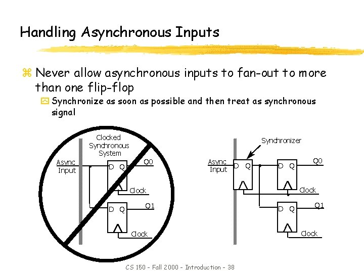
Handling Asynchronous Inputs z Never allow asynchronous inputs to fan-out to more than one flip-flop y Synchronize as soon as possible and then treat as synchronous signal Clocked Synchronous System Async Input D Q Synchronizer Q 0 Async Input D Q Clock D Q Q 1 Clock CS 150 - Fall 2000 - Introduction - 38 Q 0 D Q Q 1 Clock

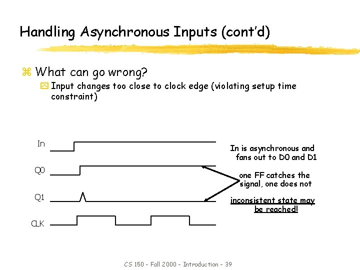
Handling Asynchronous Inputs (cont’d) z What can go wrong? y Input changes too close to clock edge (violating setup time constraint) In In is asynchronous and fans out to D 0 and D 1 Q 0 one FF catches the signal, one does not Q 1 inconsistent state may be reached! CLK CS 150 - Fall 2000 - Introduction - 39

Flip-Flop Features z Pretty important stuff z Make sure you know y Set, Reset x. Synchronous, Asynchronous, and their differences y Enable y How timing analysis works when these features are added CS 150 - Fall 2000 - Introduction - 40

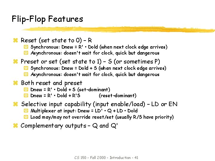
Flip-Flop Features z Reset (set state to 0) – R y Synchronous: Dnew = R' • Dold (when next clock edge arrives) y Asynchronous: doesn't wait for clock, quick but dangerous z Preset or set (set state to 1) – S (or sometimes P) y Synchronous: Dnew = Dold + S (when next clock edge arrives) y Asynchronous: doesn't wait for clock, quick but dangerous z Both reset and preset y Dnew = R' • Dold + S (set-dominant) y Dnew = R' • Dold + R'S (reset-dominant) z Selective input capability (input enable/load) – LD or EN y Multiplexer at input: Dnew = LD' • Q + LD • Dold y Load may/may not override reset/set (usually R/S have priority) z Complementary outputs – Q and Q' CS 150 - Fall 2000 - Introduction - 41

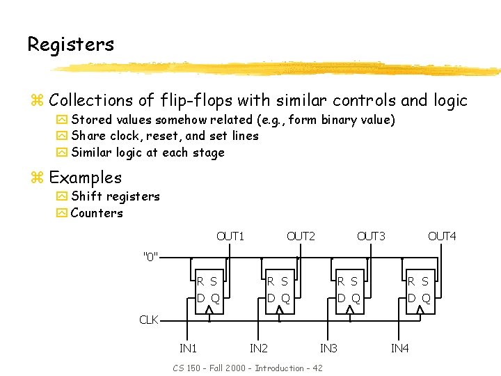
Registers z Collections of flip-flops with similar controls and logic y Stored values somehow related (e. g. , form binary value) y Share clock, reset, and set lines y Similar logic at each stage z Examples y Shift registers y Counters OUT 1 OUT 2 OUT 3 OUT 4 "0" R S D Q CLK IN 1 IN 2 IN 3 CS 150 - Fall 2000 - Introduction - 42 IN 4

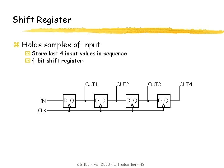
Shift Register z Holds samples of input y Store last 4 input values in sequence y 4 -bit shift register: OUT 1 IN D Q OUT 2 D Q CLK CS 150 - Fall 2000 - Introduction - 43 OUT 3 D Q OUT 4

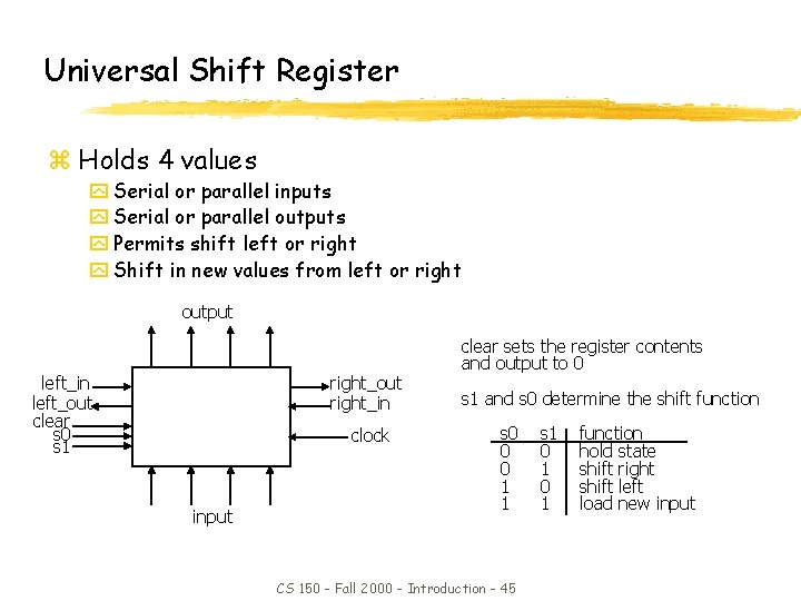
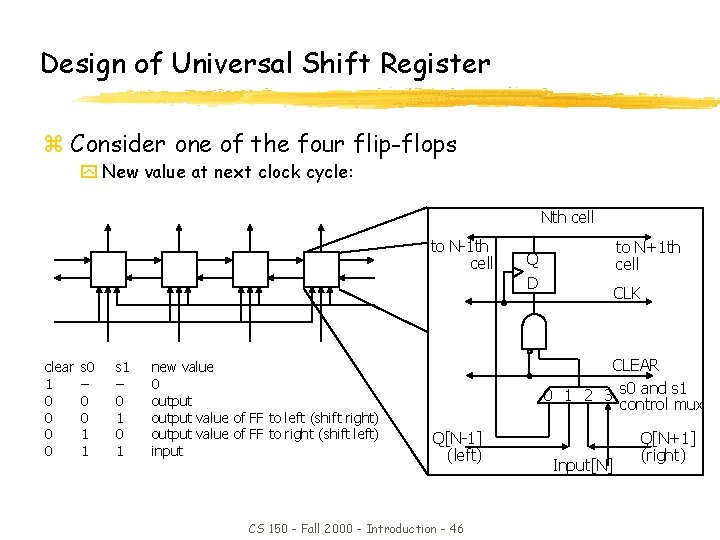
Universal Shift Register z A good Case study z Take a good look at it z Make sure you know how it works CS 150 - Fall 2000 - Introduction - 44

Universal Shift Register z Holds 4 values y Serial or parallel inputs y Serial or parallel outputs y Permits shift left or right y Shift in new values from left or right output left_in left_out clear s 0 s 1 right_out right_in clock input clear sets the register contents and output to 0 s 1 and s 0 determine the shift function s 0 0 0 1 1 CS 150 - Fall 2000 - Introduction - 45 s 1 0 1 function hold state shift right shift left load new input

Design of Universal Shift Register z Consider one of the four flip-flops y New value at next clock cycle: Nth cell to N-1 th cell clear 1 0 0 s 0 – 0 0 1 1 s 1 – 0 1 new value 0 output value of FF to left (shift right) output value of FF to right (shift left) input to N+1 th cell Q D CLK CLEAR 0 1 2 3 s 0 and s 1 control mux Q[N-1] (left) CS 150 - Fall 2000 - Introduction - 46 Input[N] Q[N+1] (right)

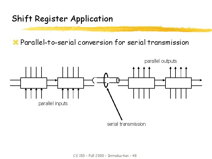
Shift Register Application z You probably don’t need to Memorize these in detail z Just look over them make sure they make sense to you CS 150 - Fall 2000 - Introduction - 47

Shift Register Application z Parallel-to-serial conversion for serial transmission parallel outputs parallel inputs serial transmission CS 150 - Fall 2000 - Introduction - 48

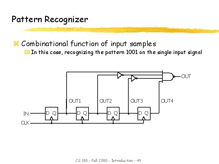
Pattern Recognizer z Combinational function of input samples y In this case, recognizing the pattern 1001 on the single input signal OUT 1 IN D Q OUT 2 D Q OUT 3 D Q CLK CS 150 - Fall 2000 - Introduction - 49 OUT 4

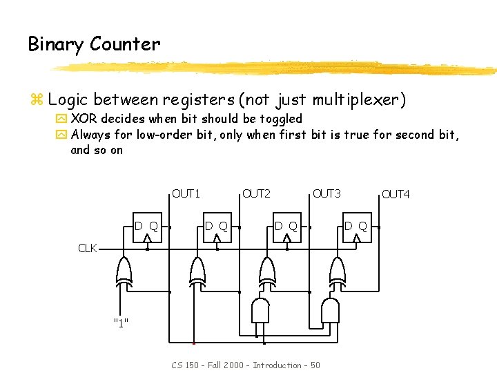
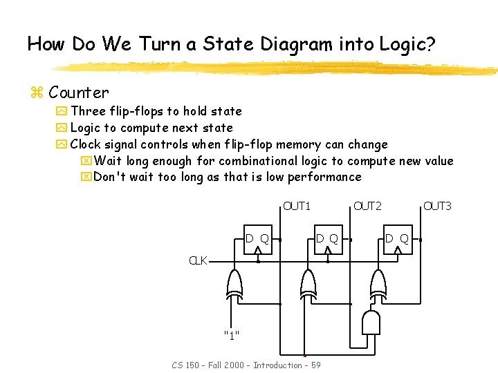
Binary Counter z Logic between registers (not just multiplexer) y XOR decides when bit should be toggled y Always for low-order bit, only when first bit is true for second bit, and so on OUT 1 D Q OUT 2 D Q OUT 3 D Q CLK "1" CS 150 - Fall 2000 - Introduction - 50 OUT 4 D Q

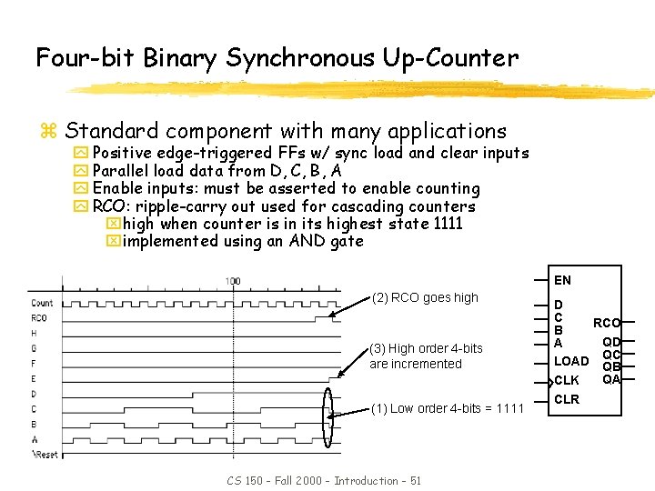
Four-bit Binary Synchronous Up-Counter z Standard component with many applications y Positive edge-triggered FFs w/ sync load and clear inputs y Parallel load data from D, C, B, A y Enable inputs: must be asserted to enable counting y RCO: ripple-carry out used for cascading counters xhigh when counter is in its highest state 1111 ximplemented using an AND gate EN (2) RCO goes high (3) High order 4 -bits are incremented (1) Low order 4 -bits = 1111 CS 150 - Fall 2000 - Introduction - 51 D C RCO B QD A QC LOAD QB QA CLK CLR

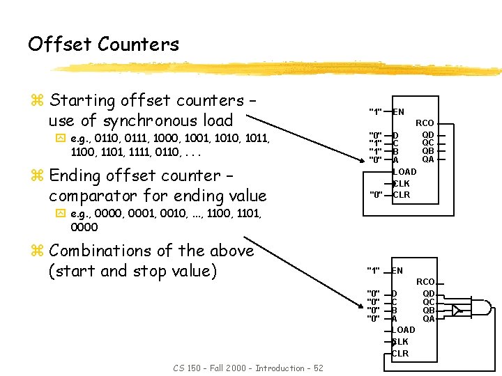
Offset Counters z Starting offset counters – use of synchronous load y e. g. , 0110, 0111, 1000, 1001, 1010, 1011, 1100, 1101, 1111, 0110, . . . z Ending offset counter – comparator for ending value "1" "0" EN RCO QD D QC C QB B QA A LOAD CLK CLR y e. g. , 0000, 0001, 0010, . . . , 1100, 1101, 0000 z Combinations of the above (start and stop value) "1" "0" "0" CS 150 - Fall 2000 - Introduction - 52 EN D C B A LOAD CLK CLR RCO QD QC QB QA

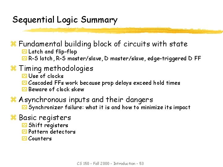
Sequential Logic Summary z Fundamental building block of circuits with state y Latch and flip-flop y R-S latch, R-S master/slave, D master/slave, edge-triggered D FF z Timing methodologies y Use of clocks y Cascaded FFs work because prop delays exceed hold times y Beware of clock skew z Asynchronous inputs and their dangers y Synchronizer failure: what it is and how to minimize its impact z Basic registers y Shift registers y Pattern detectors y Counters CS 150 - Fall 2000 - Introduction - 53

Sequential Logic Implementation z Ah… FSMs… z Another one of those things that you’d better make sure you know for the midterm. z (that means at least one problem related to it on the test) CS 150 - Fall 2000 - Introduction - 54

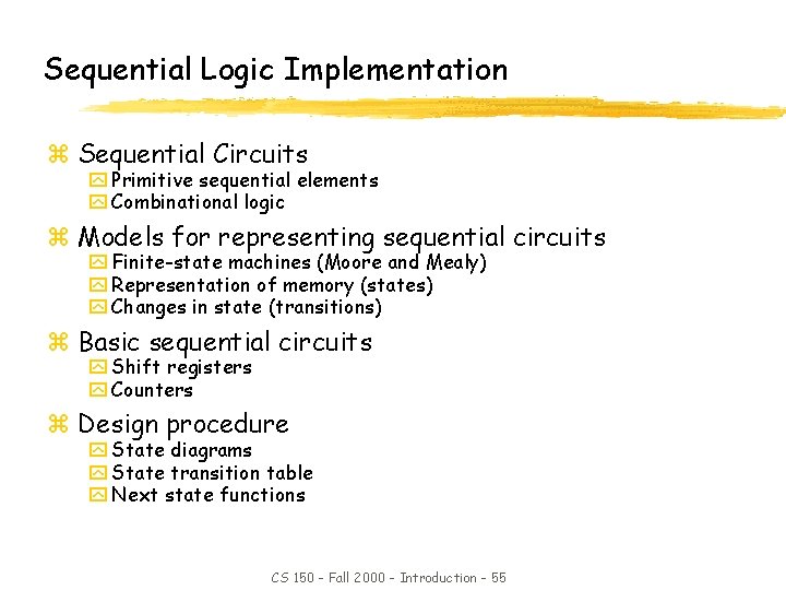
Sequential Logic Implementation z Sequential Circuits y Primitive sequential elements y Combinational logic z Models for representing sequential circuits y Finite-state machines (Moore and Mealy) y Representation of memory (states) y Changes in state (transitions) z Basic sequential circuits y Shift registers y Counters z Design procedure y State diagrams y State transition table y Next state functions CS 150 - Fall 2000 - Introduction - 55

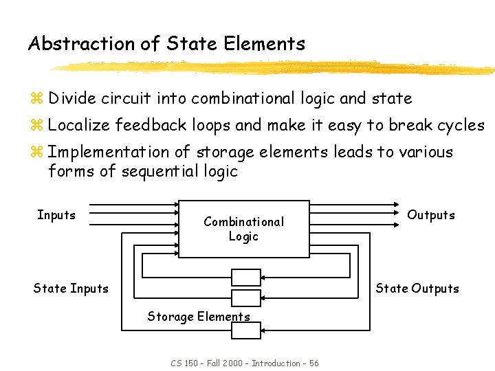
Abstraction of State Elements z Divide circuit into combinational logic and state z Localize feedback loops and make it easy to break cycles z Implementation of storage elements leads to various forms of sequential logic Inputs Combinational Logic State Inputs Outputs State Outputs Storage Elements CS 150 - Fall 2000 - Introduction - 56

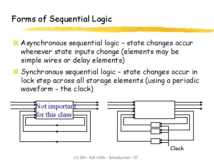
Forms of Sequential Logic z Asynchronous sequential logic – state changes occur whenever state inputs change (elements may be simple wires or delay elements) z Synchronous sequential logic – state changes occur in lock step across all storage elements (using a periodic waveform - the clock) Not important for this class Clock CS 150 - Fall 2000 - Introduction - 57

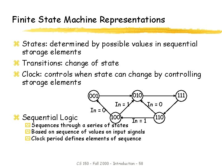
Finite State Machine Representations z States: determined by possible values in sequential storage elements z Transitions: change of state z Clock: controls when state can change by controlling storage elements 010 001 z Sequential Logic In = 0 In = 1 100 In = 1 y Sequences through a series of states y Based on sequence of values on input signals y Clock period defines elements of sequence CS 150 - Fall 2000 - Introduction - 58 111 In = 0 110

How Do We Turn a State Diagram into Logic? z Counter y Three flip-flops to hold state y Logic to compute next state y Clock signal controls when flip-flop memory can change x. Wait long enough for combinational logic to compute new value x. Don't wait too long as that is low performance OUT 1 D Q OUT 2 D Q CLK "1" CS 150 - Fall 2000 - Introduction - 59 OUT 3 D Q

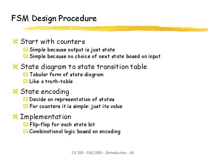
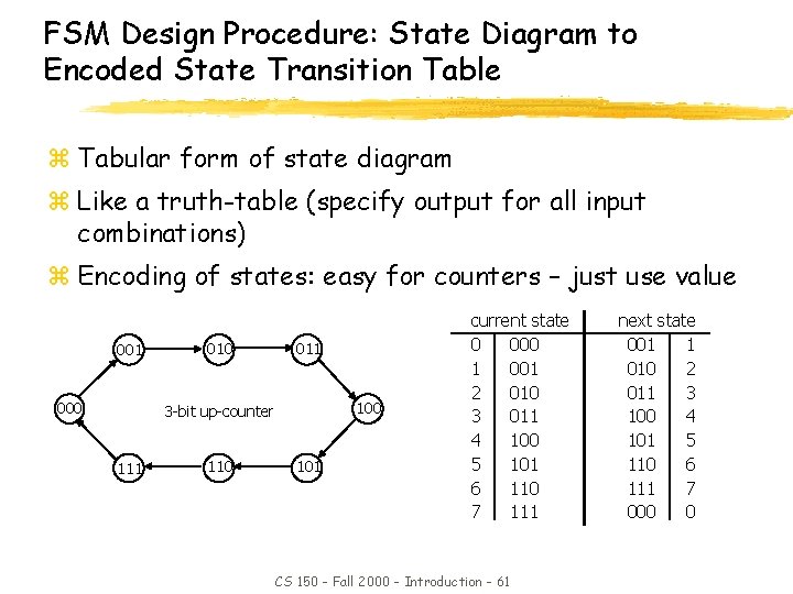
FSM Design Procedure z Start with counters y Simple because output is just state y Simple because no choice of next state based on input z State diagram to state transition table y Tabular form of state diagram y Like a truth-table z State encoding y Decide on representation of states y For counters it is simple: just its value z Implementation y Flip-flop for each state bit y Combinational logic based on encoding CS 150 - Fall 2000 - Introduction - 60

FSM Design Procedure: State Diagram to Encoded State Transition Table z Tabular form of state diagram z Like a truth-table (specify output for all input combinations) z Encoding of states: easy for counters – just use value 001 000 011 100 3 -bit up-counter 111 110 101 current state 0 000 1 001 2 010 3 011 4 100 5 101 6 110 7 111 CS 150 - Fall 2000 - Introduction - 61 next state 001 1 010 2 011 3 100 4 101 5 110 6 111 7 000 0

Implementation z Really important MAKE SURE you know how to implement FSM, all the way from word descriptions to circuit implementation. z However don’t go and memorize all the different implementations. (there are too many slides) z Instead concentrate on how to do it yourself. CS 150 - Fall 2000 - Introduction - 62

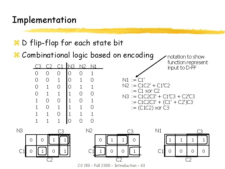
Implementation z D flip-flop for each state bit z Combinational logic based on encoding C 3 0 0 1 1 C 2 0 0 1 1 C 1 0 1 0 1 N 3 0 0 0 1 1 0 C 3 N 2 0 1 1 0 N 1 1 0 1 0 notation to show function represent input to D-FF N 1 : = C 1' N 2 : = C 1 C 2' + C 1'C 2 : = C 1 xor C 2 N 3 : = C 1 C 2 C 3' + C 1'C 3 + C 2'C 3 : = C 1 C 2 C 3' + (C 1' + C 2')C 3 : = (C 1 C 2) xor C 3 N 2 C 3 N 1 C 3 0 0 1 1 C 1 0 1 C 1 1 0 0 1 C 1 0 0 C 2 CS 150 - Fall 2000 - Introduction - 63 C 2

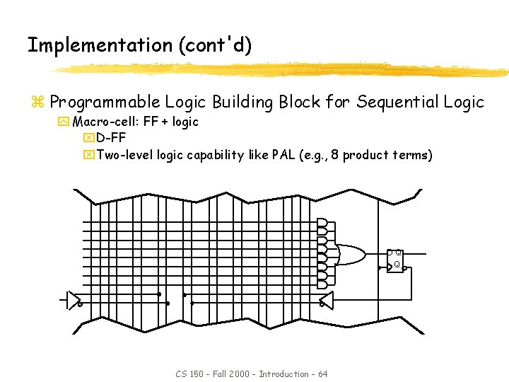
Implementation (cont'd) z Programmable Logic Building Block for Sequential Logic y Macro-cell: FF + logic x. D-FF x. Two-level logic capability like PAL (e. g. , 8 product terms) DQ Q CS 150 - Fall 2000 - Introduction - 64

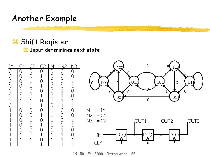
Another Example z Shift Register y Input determines next state In 0 0 0 0 1 1 1 1 C 1 0 0 0 0 1 1 1 1 C 2 0 0 1 1 C 3 0 1 0 1 N 1 0 0 0 0 1 1 1 1 N 2 0 0 0 0 1 1 1 1 N 3 0 0 1 1 1 100 0 101 0 0 001 N 1 : = In N 2 : = C 1 N 3 : = C 2 IN 0 OUT 1 D Q CLK CS 150 - Fall 2000 - Introduction - 65 1 1 1 010 1 000 110 D Q 111 0 011 OUT 2 D Q OUT 3 1

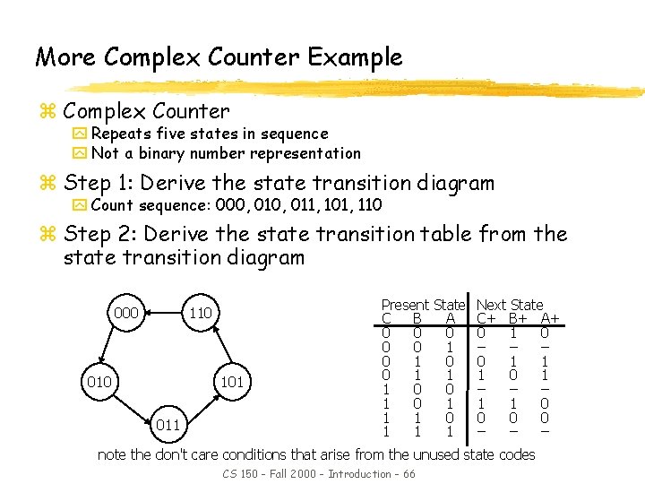
More Complex Counter Example z Complex Counter y Repeats five states in sequence y Not a binary number representation z Step 1: Derive the state transition diagram y Count sequence: 000, 011, 101, 110 z Step 2: Derive the state transition table from the state transition diagram 000 110 010 101 011 Present State Next State C B A C+ B+ A+ 0 0 1 0 0 0 1 – – – 0 1 0 0 1 1 1 0 0 – – – 1 0 1 1 0 0 1 1 1 – – – note the don't care conditions that arise from the unused state codes CS 150 - Fall 2000 - Introduction - 66

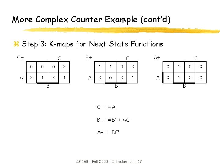
More Complex Counter Example (cont’d) z Step 3: K-maps for Next State Functions C+ A B+ C 0 0 0 X X 1 B A A+ C 1 1 0 X X 0 X 1 B C+ : = A B+ : = B' + A'C' A+ : = BC' CS 150 - Fall 2000 - Introduction - 67 A C 0 1 0 X X 1 X 0 B

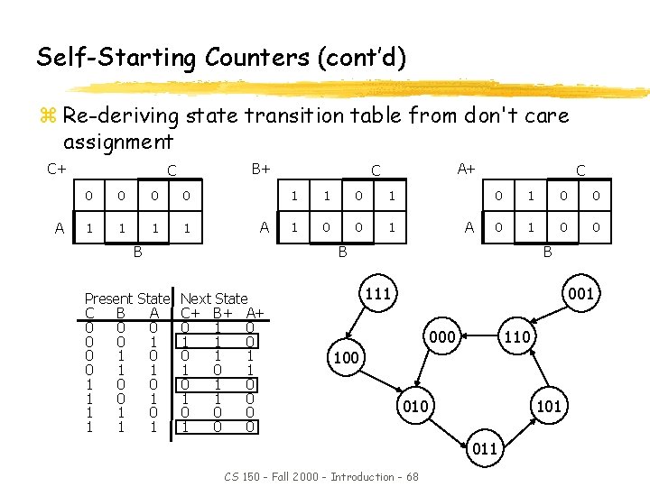
Self-Starting Counters (cont’d) z Re-deriving state transition table from don't care assignment C+ A B+ C 0 0 1 1 A A+ C 1 1 0 0 1 A C 0 1 0 0 B B Present State Next State C B A C+ B+ A+ 0 0 1 0 0 0 1 1 1 0 0 1 1 0 0 0 1 0 1 1 1 0 0 0 0 1 1 0 0 B 111 000 110 100 010 101 011 CS 150 - Fall 2000 - Introduction - 68

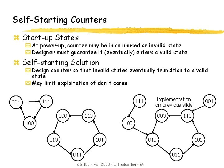
Self-Starting Counters z Start-up States y At power-up, counter may be in an unused or invalid state y Designer must guarantee it (eventually) enters a valid state z Self-starting Solution y Design counter so that invalid states eventually transition to a valid state y May limit exploitation of don't cares 111 001 000 implementation on previous slide 000 110 001 110 100 010 101 011 CS 150 - Fall 2000 - Introduction - 69 010 101 011

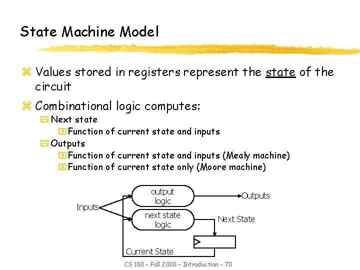
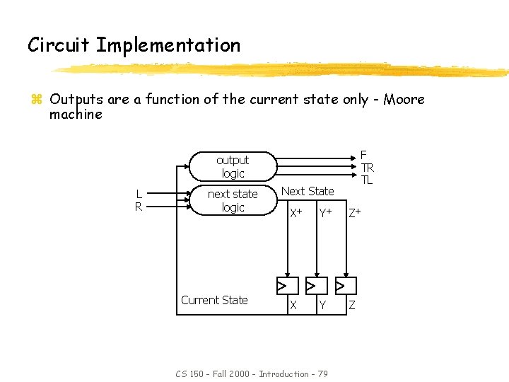
State Machine Model z Values stored in registers represent the state of the circuit z Combinational logic computes: y Next state x. Function of current state and inputs y Outputs x. Function of current state and inputs (Mealy machine) x. Function of current state only (Moore machine) Inputs output logic next state logic Outputs Next State Current State CS 150 - Fall 2000 - Introduction - 70

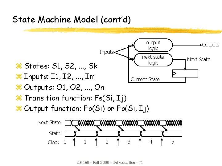
State Machine Model (cont’d) output logic Inputs Outputs next state logic Next State z States: S 1, S 2, . . . , Sk z Inputs: I 1, I 2, . . . , Im Current State z Outputs: O 1, O 2, . . . , On z Transition function: Fs(Si, Ij) z Output function: Fo(Si) or Fo(Si, Ij) Next State Clock 0 1 2 3 CS 150 - Fall 2000 - Introduction - 71 4 5

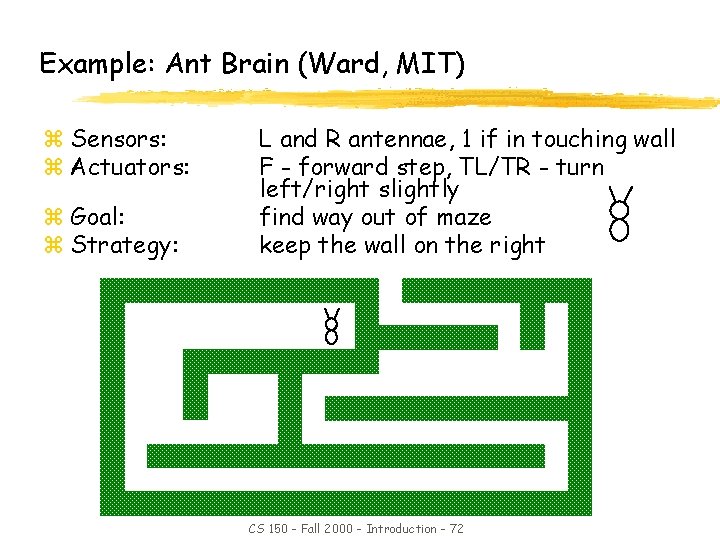
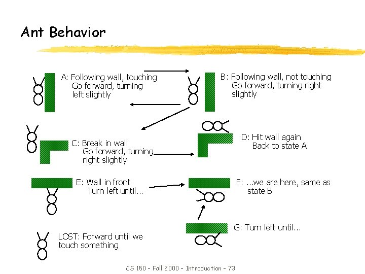
Example: Ant Brain (Ward, MIT) z Sensors: z Actuators: z Goal: z Strategy: L and R antennae, 1 if in touching wall F - forward step, TL/TR - turn left/right slightly find way out of maze keep the wall on the right CS 150 - Fall 2000 - Introduction - 72

Ant Behavior A: Following wall, touching Go forward, turning left slightly B: Following wall, not touching Go forward, turning right slightly D: Hit wall again Back to state A C: Break in wall Go forward, turning right slightly E: Wall in front Turn left until. . . LOST: Forward until we touch something F: . . . we are here, same as state B G: Turn left until. . . CS 150 - Fall 2000 - Introduction - 73

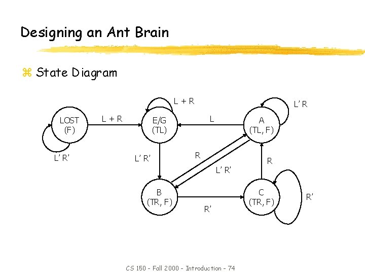
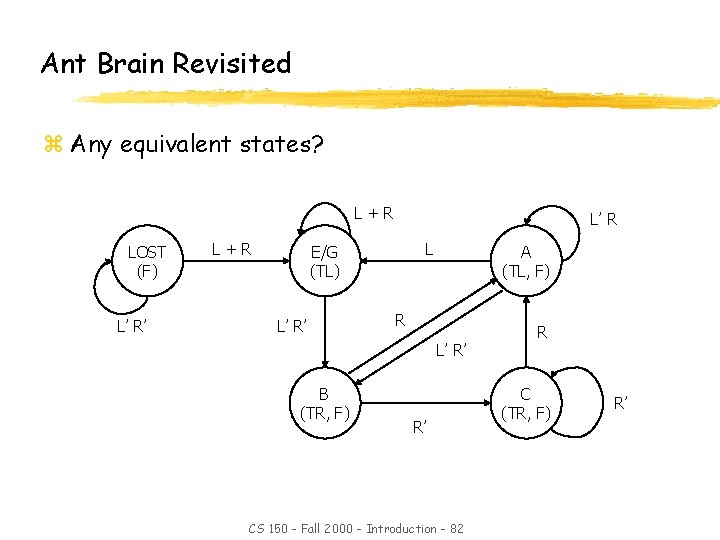
Designing an Ant Brain z State Diagram L+R LOST (F) L’ R’ L+R L’ R L E/G (TL) L’ R’ A (TL, F) R L’ R’ B (TR, F) R’ CS 150 - Fall 2000 - Introduction - 74 R C (TR, F) R’

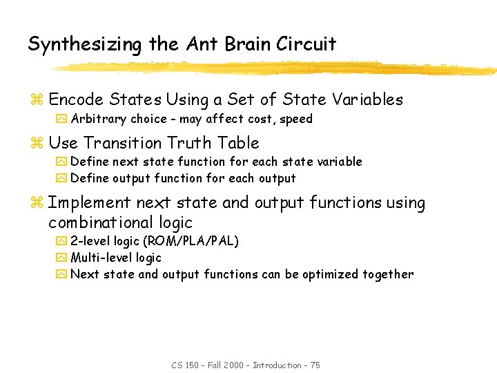
Synthesizing the Ant Brain Circuit z Encode States Using a Set of State Variables y Arbitrary choice - may affect cost, speed z Use Transition Truth Table y Define next state function for each state variable y Define output function for each output z Implement next state and output functions using combinational logic y 2 -level logic (ROM/PLA/PAL) y Multi-level logic y Next state and output functions can be optimized together CS 150 - Fall 2000 - Introduction - 75

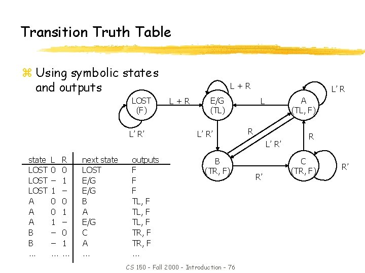
Transition Truth Table z Using symbolic states and outputs LOST (F) L’ R’ L+R E/G (TL) L’ R’ L’ R A (TL, F) L R L’ R’ state LOST A A A B B. . . L 0 – 1 0 0 1 – –. . . R 0 1 – 0 1. . . next state LOST E/G B A E/G C A. . . outputs F F F TL, F TR, F. . . B (TR, F) CS 150 - Fall 2000 - Introduction - 76 R’ R C (TR, F) R’

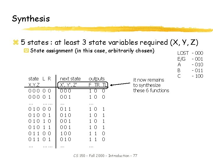
Synthesis z 5 states : at least 3 state variables required (X, Y, Z) y State assignment (in this case, arbitrarily chosen) state X, Y, Z 000. . . 010 010 011. . . L R 0 0 0 1. . . 0 0 0 1 1 0 0 0 1. . . next state X', Y', Z' 000 001. . . 011 010 001 100 010. . . outputs F TR TL 1 0 0. . . 1 0 1 1 1 0. . . it now remains to synthesize these 6 functions CS 150 - Fall 2000 - Introduction - 77 LOST E/G A B C - 000 001 010 011 100

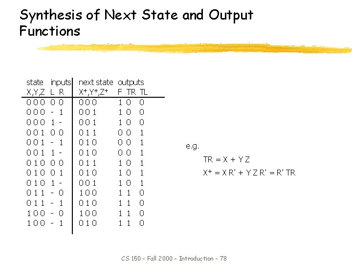
Synthesis of Next State and Output Functions state X, Y, Z 000 000 001 001 010 010 011 100 inputs L R 0 0 - 1 1 0 0 0 1 1 - 0 - 1 next state X+, Y+, Z+ 000 001 011 010 001 100 010 outputs F TR TL 1 0 0 1 0 0 1 1 0 1 1 0 e. g. TR = X + Y Z X+ = X R’ + Y Z R’ = R’ TR CS 150 - Fall 2000 - Introduction - 78

Circuit Implementation z Outputs are a function of the current state only - Moore machine F TR TL output logic L R next state logic Current State Next State X+ Y+ Z+ X Y Z CS 150 - Fall 2000 - Introduction - 79

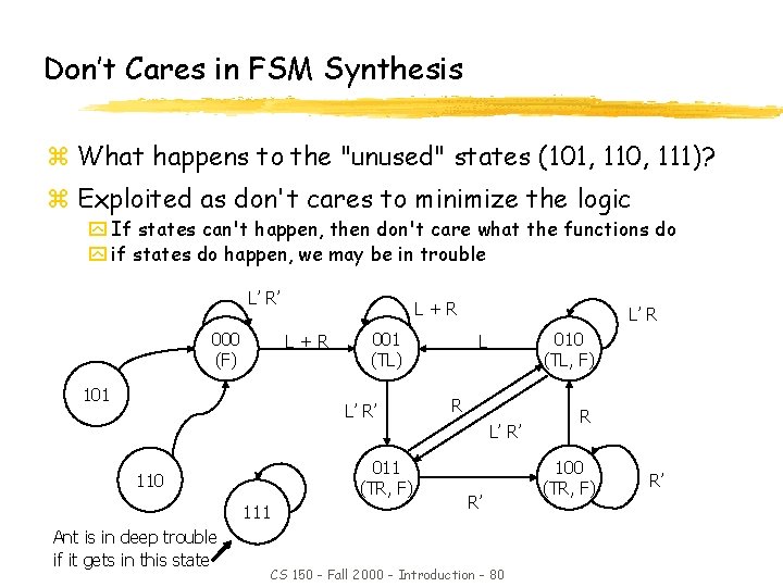
Don’t Cares in FSM Synthesis z What happens to the "unused" states (101, 110, 111)? z Exploited as don't cares to minimize the logic y If states can't happen, then don't care what the functions do y if states do happen, we may be in trouble L’ R’ 000 (F) L+R 101 001 (TL) L’ R’ L’ R 010 (TL, F) L R L’ R’ 011 (TR, F) 110 111 Ant is in deep trouble if it gets in this state R’ CS 150 - Fall 2000 - Introduction - 80 R 100 (TR, F) R’

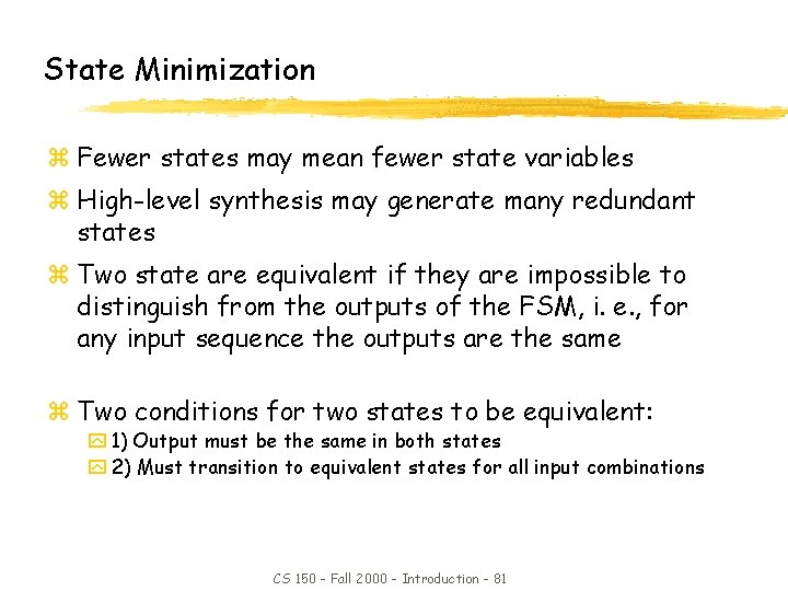
State Minimization z Fewer states may mean fewer state variables z High-level synthesis may generate many redundant states z Two state are equivalent if they are impossible to distinguish from the outputs of the FSM, i. e. , for any input sequence the outputs are the same z Two conditions for two states to be equivalent: y 1) Output must be the same in both states y 2) Must transition to equivalent states for all input combinations CS 150 - Fall 2000 - Introduction - 81

Ant Brain Revisited z Any equivalent states? L+R LOST (F) L’ R’ L+R L’ R L E/G (TL) L’ R’ A (TL, F) R L’ R’ B (TR, F) R’ CS 150 - Fall 2000 - Introduction - 82 R C (TR, F) R’

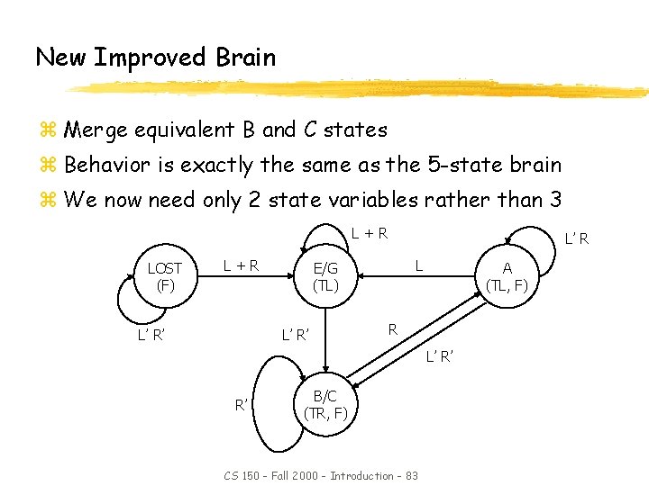
New Improved Brain z Merge equivalent B and C states z Behavior is exactly the same as the 5 -state brain z We now need only 2 state variables rather than 3 L+R LOST (F) L+R L’ R’ L’ R L E/G (TL) L’ R’ A (TL, F) R L’ R’ R’ B/C (TR, F) CS 150 - Fall 2000 - Introduction - 83

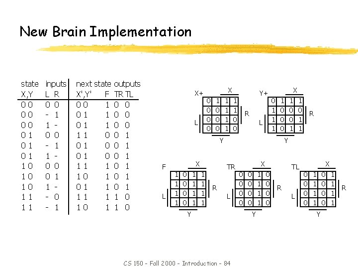
New Brain Implementation state X, Y 00 00 00 01 01 01 10 10 10 11 11 inputs L R 0 0 - 1 1 0 0 0 1 1 - 0 - 1 next state outputs X', Y' F TR TL 00 1 0 0 01 1 0 0 1 01 0 0 1 11 1 0 1 10 1 01 1 0 1 11 1 1 0 10 1 1 0 X+ L X 0 0 1 0 0 0 1 1 Y+ 1 1 0 0 R L X 0 1 1 0 0 0 Y F L X 1 1 0 0 1 1 1 1 1 0 0 1 1 R Y TR R L Y CS 150 - Fall 2000 - Introduction - 84 X 0 0 0 0 1 1 Y 0 0 TL R L X 0 0 1 1 0 0 Y 1 1 R

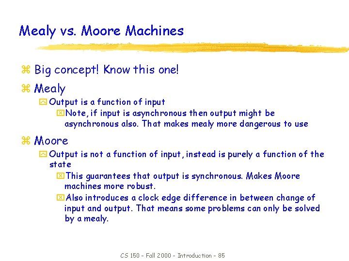
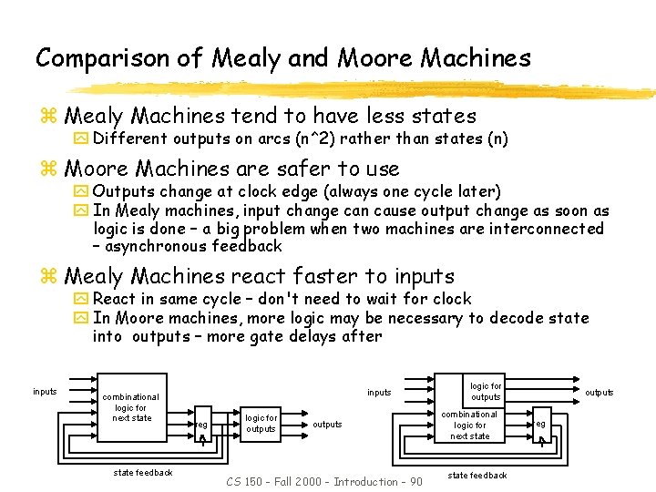
Mealy vs. Moore Machines z Big concept! Know this one! z Mealy y Output is a function of input x. Note, if input is asynchronous then output might be asynchronous also. That makes mealy more dangerous to use z Moore y Output is not a function of input, instead is purely a function of the state x. This guarantees that output is synchronous. Makes Moore machines more robust. x. Also introduces a clock edge difference in between change of input and output. That means some problems can only be solved by a mealy. CS 150 - Fall 2000 - Introduction - 85

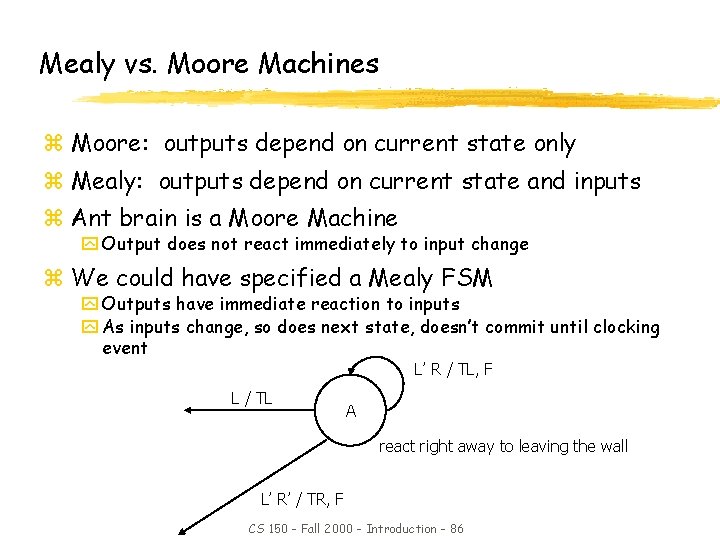
Mealy vs. Moore Machines z Moore: outputs depend on current state only z Mealy: outputs depend on current state and inputs z Ant brain is a Moore Machine y Output does not react immediately to input change z We could have specified a Mealy FSM y Outputs have immediate reaction to inputs y As inputs change, so does next state, doesn’t commit until clocking event L’ R / TL, F L / TL A react right away to leaving the wall L’ R’ / TR, F CS 150 - Fall 2000 - Introduction - 86

Arg… So many slides of examples! z Again don’t kill yourself trying to memorize every detail of these examples z Just make sure they make sense to you CS 150 - Fall 2000 - Introduction - 87

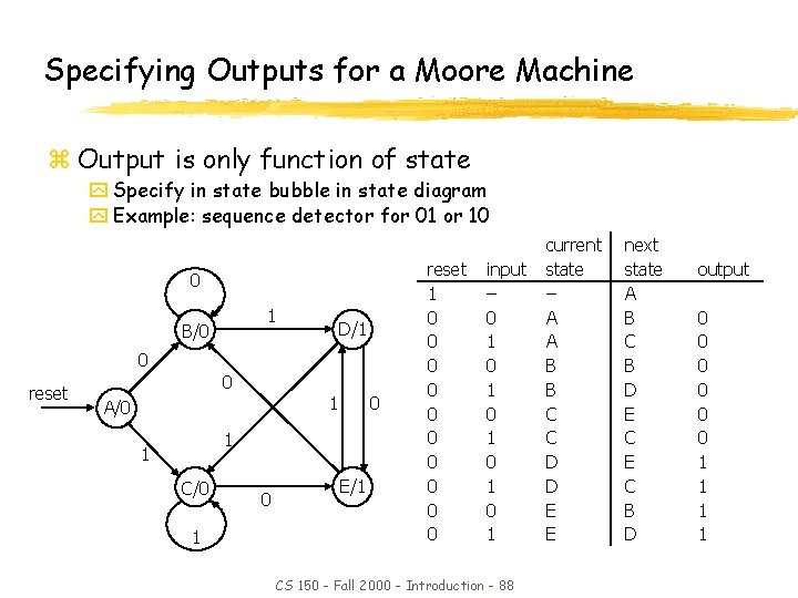
Specifying Outputs for a Moore Machine z Output is only function of state y Specify in state bubble in state diagram y Example: sequence detector for 01 or 10 0 1 B/0 D/1 0 reset 0 1 A/0 0 1 1 C/0 1 0 E/1 reset 1 0 0 0 0 0 input – 0 1 0 1 0 1 CS 150 - Fall 2000 - Introduction - 88 current state – A A B B C C D D E E next state A B C B D E C B D output 0 0 0 1 1

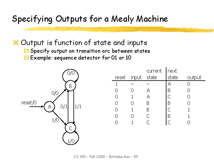
Specifying Outputs for a Mealy Machine z Output is function of state and inputs y Specify output on transition arc between states y Example: sequence detector for 01 or 10 0/0 B 0/0 reset/0 0/1 A 1/1 1/0 reset 1 0 0 0 input – 0 1 0 1 C 1/0 CS 150 - Fall 2000 - Introduction - 89 current state – A A B B C C next state A B C B C output 0 0 1 1 0

Comparison of Mealy and Moore Machines z Mealy Machines tend to have less states y Different outputs on arcs (n^2) rather than states (n) z Moore Machines are safer to use y Outputs change at clock edge (always one cycle later) y In Mealy machines, input change can cause output change as soon as logic is done – a big problem when two machines are interconnected – asynchronous feedback z Mealy Machines react faster to inputs y React in same cycle – don't need to wait for clock y In Moore machines, more logic may be necessary to decode state into outputs – more gate delays after inputs combinational logic for next state feedback inputs reg logic for outputs CS 150 - Fall 2000 - Introduction - 90 logic for outputs combinational logic for next state feedback outputs reg

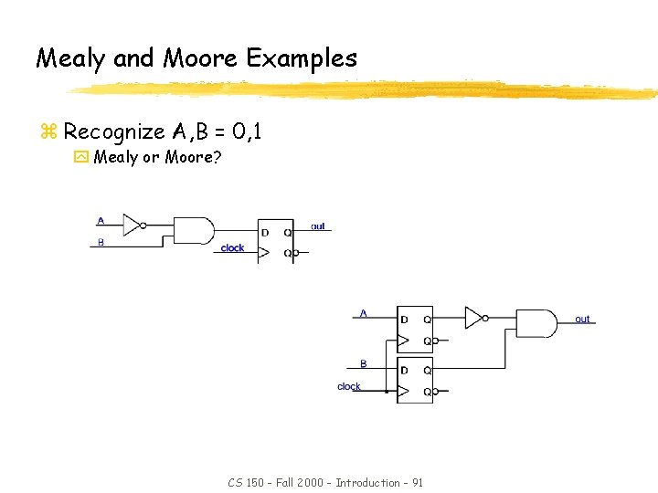
Mealy and Moore Examples z Recognize A, B = 0, 1 y Mealy or Moore? CS 150 - Fall 2000 - Introduction - 91

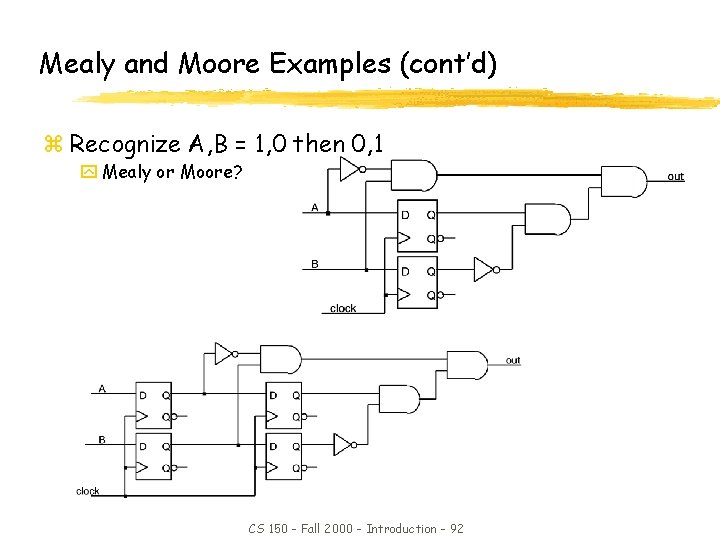
Mealy and Moore Examples (cont’d) z Recognize A, B = 1, 0 then 0, 1 y Mealy or Moore? CS 150 - Fall 2000 - Introduction - 92

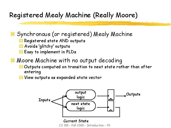
Registered Mealy Machine (Really Moore) z Synchronous (or registered) Mealy Machine y Registered state AND outputs y Avoids ‘glitchy’ outputs y Easy to implement in PLDs z Moore Machine with no output decoding y Outputs computed on transition to next state rather than after entering y View outputs as expanded state vector Inputs output logic next state logic Current State CS 150 - Fall 2000 - Introduction - 93 Outputs

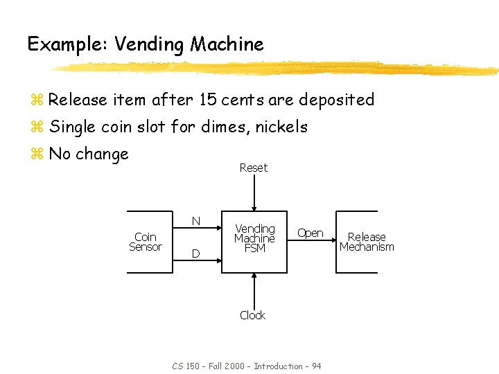
Example: Vending Machine z Release item after 15 cents are deposited z Single coin slot for dimes, nickels z No change Reset N Coin Sensor D Vending Machine FSM Open Clock CS 150 - Fall 2000 - Introduction - 94 Release Mechanism

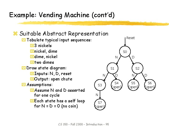
Example: Vending Machine (cont’d) z Suitable Abstract Representation y Tabulate typical input sequences: x 3 nickels xnickel, dime xdime, nickel xtwo dimes y Draw state diagram: x. Inputs: N, D, reset x. Output: open chute y Assumptions: x. Assume N and D asserted for one cycle x. Each state has a self loop for N = D = 0 (no coin) Reset S 0 N D S 1 N S 3 N S 7 [open] CS 150 - Fall 2000 - Introduction - 95 S 2 D N S 4 [open] S 5 [open] D S 6 [open]

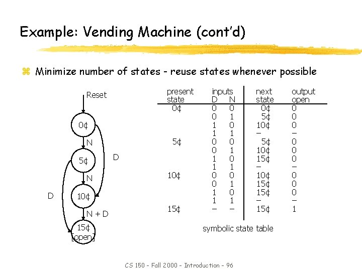
Example: Vending Machine (cont’d) z Minimize number of states - reuse states whenever possible present state 0¢ Reset 0¢ 5¢ N D D 10¢ N+D 15¢ [open] 15¢ inputs D N 0 0 0 1 1 0 0 0 1 1 – – next state 0¢ 5¢ 10¢ – 5¢ 10¢ 15¢ – 15¢ symbolic state table CS 150 - Fall 2000 - Introduction - 96 output open 0 0 0 – 1

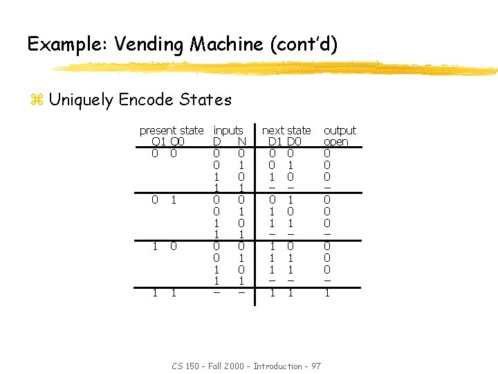
Example: Vending Machine (cont’d) z Uniquely Encode States present state inputs Q 1 Q 0 D N 0 0 0 1 1 0 1 0 0 0 1 1 1 0 0 1 1 – – next D 1 0 0 1 – 0 1 1 – 1 state D 0 0 1 0 – 1 0 1 – 0 1 1 – 1 CS 150 - Fall 2000 - Introduction - 97 output open 0 0 0 – 1

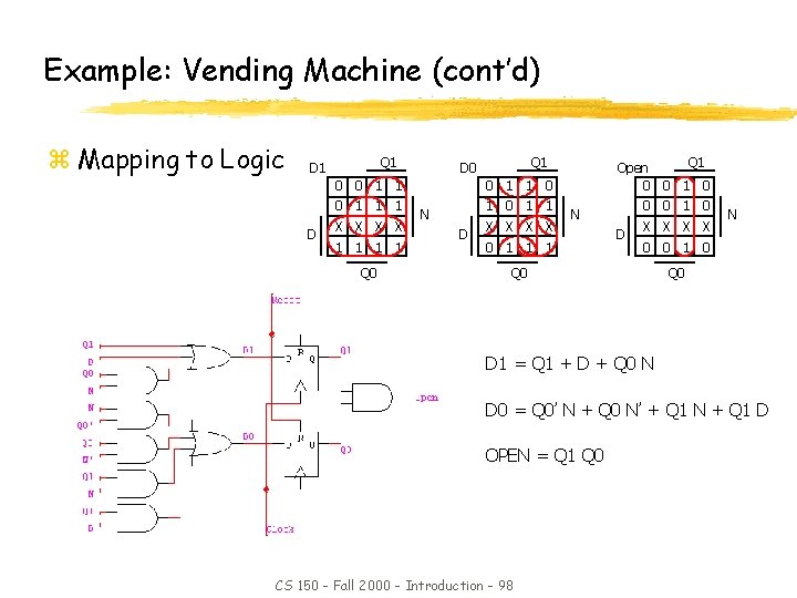
Example: Vending Machine (cont’d) z Mapping to Logic Q 1 D 1 0 0 1 1 1 D X X 1 1 Q 0 Q 1 D 0 Q 1 Open 0 0 1 1 N D X X 0 0 1 0 N 0 1 1 1 D X X N 0 0 1 0 Q 0 D 1 = Q 1 + D + Q 0 N D 0 = Q 0’ N + Q 0 N’ + Q 1 N + Q 1 D OPEN = Q 1 Q 0 CS 150 - Fall 2000 - Introduction - 98

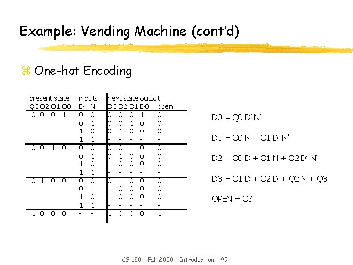
Example: Vending Machine (cont’d) z One-hot Encoding present state Q 3 Q 2 Q 1 Q 0 0 1 0 0 0 1 1 0 0 0 inputs D N 0 0 0 1 1 0 0 0 1 1 - - next state D 3 D 2 D 1 0 0 0 1 0 - - 0 0 1 0 1 0 0 - - 0 1 0 0 - - 1 0 0 output D 0 open 1 0 0 0 0 0 1 D 0 = Q 0 D’ N’ D 1 = Q 0 N + Q 1 D’ N’ D 2 = Q 0 D + Q 1 N + Q 2 D’ N’ D 3 = Q 1 D + Q 2 N + Q 3 OPEN = Q 3 CS 150 - Fall 2000 - Introduction - 99

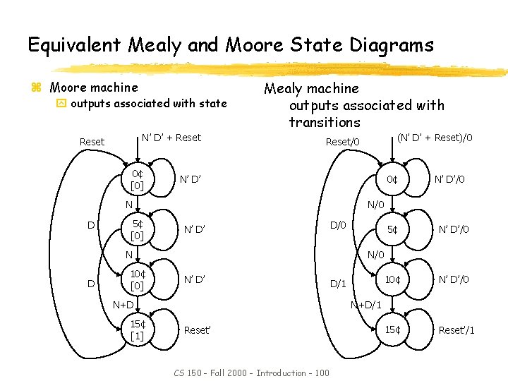
Equivalent Mealy and Moore State Diagrams z Moore machine y outputs associated with state N’ D’ + Reset 0¢ [0] Mealy machine outputs associated with transitions 0¢ N’ D’ N D 5¢ [0] 10¢ [0] N’ D’ D/0 5¢ N’ D’/0 10¢ N’ D’/0 15¢ Reset’/1 N/0 N’ D’ N+D 15¢ [1] N’ D’/0 N D (N’ D’ + Reset)/0 Reset/0 D/1 N+D/1 Reset’ CS 150 - Fall 2000 - Introduction - 100

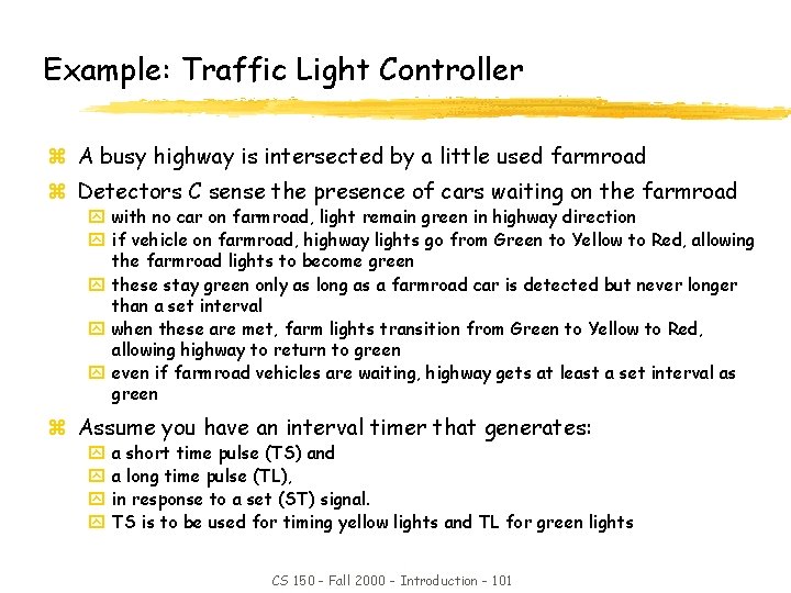
Example: Traffic Light Controller z A busy highway is intersected by a little used farmroad z Detectors C sense the presence of cars waiting on the farmroad y with no car on farmroad, light remain green in highway direction y if vehicle on farmroad, highway lights go from Green to Yellow to Red, allowing the farmroad lights to become green y these stay green only as long as a farmroad car is detected but never longer than a set interval y when these are met, farm lights transition from Green to Yellow to Red, allowing highway to return to green y even if farmroad vehicles are waiting, highway gets at least a set interval as green z Assume you have an interval timer that generates: y y a short time pulse (TS) and a long time pulse (TL), in response to a set (ST) signal. TS is to be used for timing yellow lights and TL for green lights CS 150 - Fall 2000 - Introduction - 101

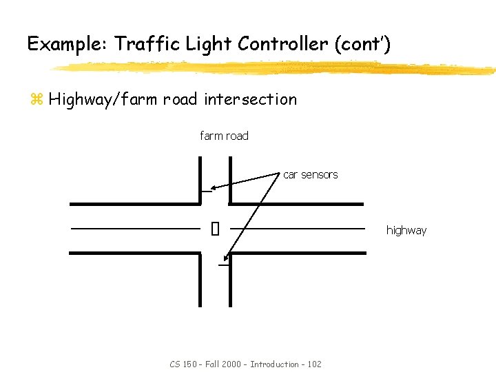
Example: Traffic Light Controller (cont’) z Highway/farm road intersection farm road car sensors highway CS 150 - Fall 2000 - Introduction - 102

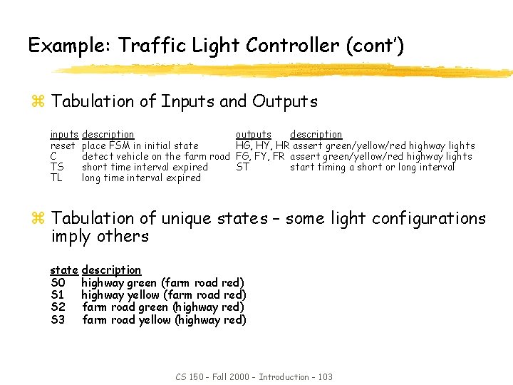
Example: Traffic Light Controller (cont’) z Tabulation of Inputs and Outputs inputs reset C TS TL description place FSM in initial state detect vehicle on the farm road short time interval expired long time interval expired outputs description HG, HY, HR assert green/yellow/red highway lights FG, FY, FR assert green/yellow/red highway lights ST start timing a short or long interval z Tabulation of unique states – some light configurations imply others state S 0 S 1 S 2 S 3 description highway green (farm road red) highway yellow (farm road red) farm road green (highway red) farm road yellow (highway red) CS 150 - Fall 2000 - Introduction - 103

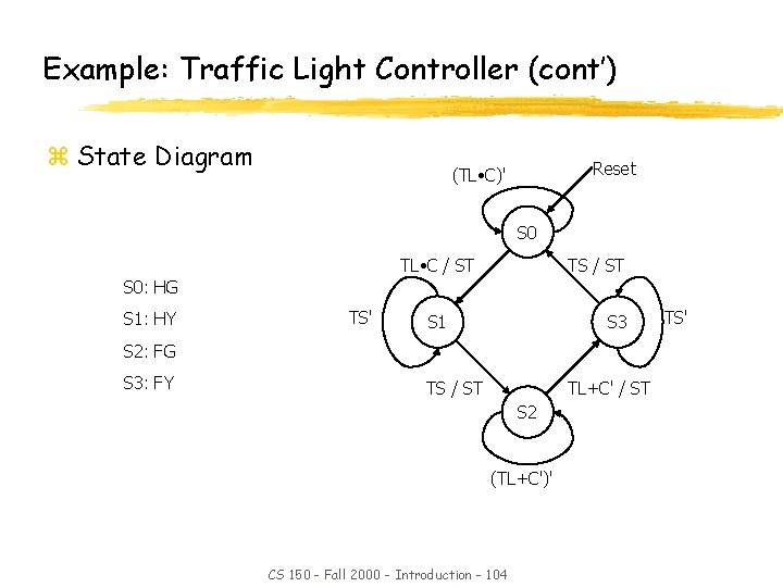
Example: Traffic Light Controller (cont’) z State Diagram Reset (TL • C)' S 0 TL • C / ST S 0: HG S 1: HY TS' TS / ST S 1 S 3 S 2: FG S 3: FY TS / ST TL+C' / ST S 2 (TL+C')' CS 150 - Fall 2000 - Introduction - 104 TS'

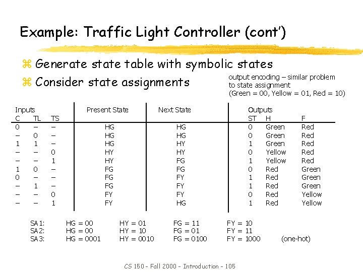
Example: Traffic Light Controller (cont’) z Generate state table with symbolic states output encoding – similar problem z Consider state assignments to state assignment (Green = 00, Yellow = 01, Red = 10) Inputs C TL 0 – – 0 1 1 – – 1 0 0 – – 1 – – SA 1: SA 2: SA 3: TS – – – 0 1 Present State HG HG HG HY HY FG FG FG FY FY HG = 0001 Next State Outputs ST H 0 Green 1 Green 0 Yellow 1 Yellow 0 Red 1 Red HG HG HY HY FG FG FY FY FY HG HY = 01 HY = 10 HY = 0010 FG = 11 FG = 0100 FY = 11 FY = 1000 CS 150 - Fall 2000 - Introduction - 105 F Red Red Red Green Yellow (one-hot)

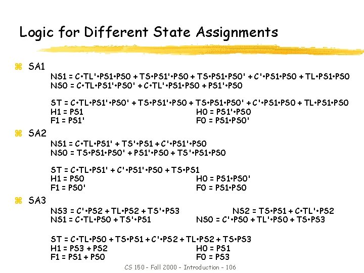
Logic for Different State Assignments z SA 1 NS 1 = C • TL' • PS 1 • PS 0 + TS • PS 1' • PS 0 + TS • PS 1 • PS 0' + C' • PS 1 • PS 0 + TL • PS 1 • PS 0 NS 0 = C • TL • PS 1' • PS 0' + C • TL' • PS 1 • PS 0 + PS 1' • PS 0 ST = C • TL • PS 1' • PS 0' + TS • PS 1' • PS 0 + TS • PS 1 • PS 0' + C' • PS 1 • PS 0 + TL • PS 1 • PS 0 H 1 = PS 1 H 0 = PS 1' • PS 0 F 1 = PS 1' F 0 = PS 1 • PS 0' z SA 2 NS 1 = C • TL • PS 1' + TS' • PS 1 + C' • PS 1' • PS 0 NS 0 = TS • PS 1 • PS 0' + PS 1' • PS 0 + TS' • PS 1 • PS 0 ST = C • TL • PS 1' + C' • PS 1' • PS 0 + TS • PS 1 H 1 = PS 0 H 0 = PS 1 • PS 0' F 1 = PS 0' F 0 = PS 1 • PS 0 z SA 3 NS 3 = C' • PS 2 + TL • PS 2 + TS' • PS 3 NS 1 = C • TL • PS 0 + TS' • PS 1 NS 2 = TS • PS 1 + C • TL' • PS 2 NS 0 = C' • PS 0 + TL' • PS 0 + TS • PS 3 ST = C • TL • PS 0 + TS • PS 1 + C' • PS 2 + TL • PS 2 + TS • PS 3 H 1 = PS 3 + PS 2 H 0 = PS 1 F 1 = PS 1 + PS 0 F 0 = PS 3 CS 150 - Fall 2000 - Introduction - 106

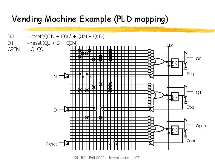
Vending Machine Example (PLD mapping) D 0 D 1 OPEN = reset'(Q 0'N + Q 0 N' + Q 1 N + Q 1 D) = reset'(Q 1 + D + Q 0 N) = Q 1 Q 0 CLK Q 0 DQ Seq N Q 1 DQ Seq D Open DQ Com Reset CS 150 - Fall 2000 - Introduction - 107

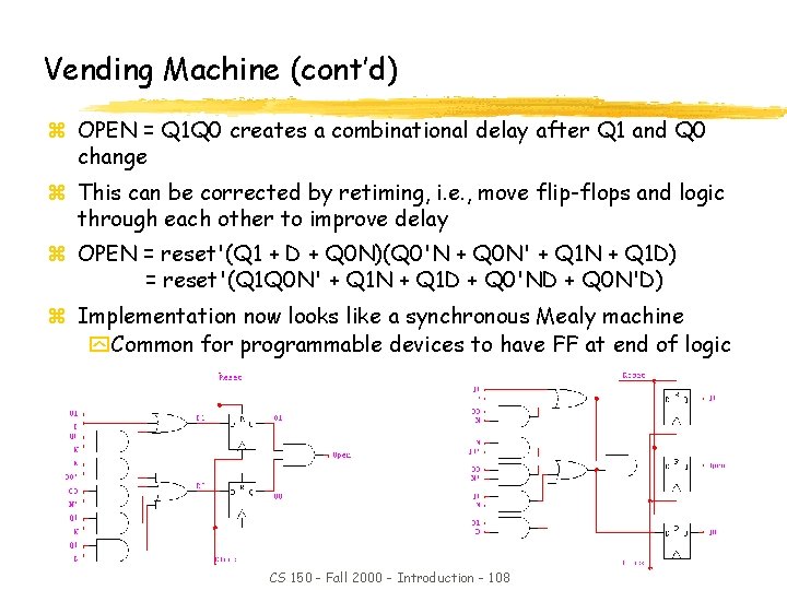
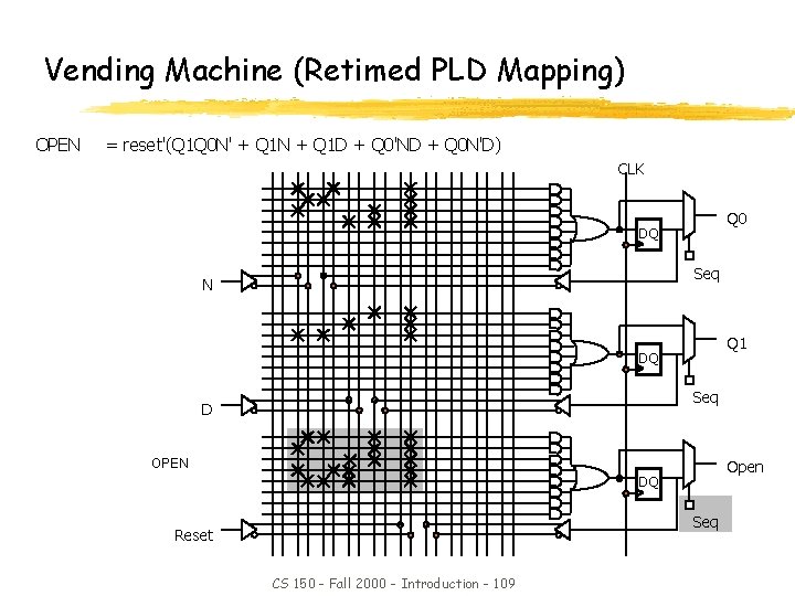
Vending Machine (cont’d) z OPEN = Q 1 Q 0 creates a combinational delay after Q 1 and Q 0 change z This can be corrected by retiming, i. e. , move flip-flops and logic through each other to improve delay z OPEN = reset'(Q 1 + D + Q 0 N)(Q 0'N + Q 0 N' + Q 1 N + Q 1 D) = reset'(Q 1 Q 0 N' + Q 1 N + Q 1 D + Q 0'ND + Q 0 N'D) z Implementation now looks like a synchronous Mealy machine y Common for programmable devices to have FF at end of logic CS 150 - Fall 2000 - Introduction - 108

Vending Machine (Retimed PLD Mapping) OPEN = reset'(Q 1 Q 0 N' + Q 1 N + Q 1 D + Q 0'ND + Q 0 N'D) CLK Q 0 DQ Seq N Q 1 DQ Seq D OPEN Open DQ Seq Reset CS 150 - Fall 2000 - Introduction - 109

Finite State Machine Optimization z Should look over this one z Make sure you know the motivation for this y State Minimization x. Try to merge state with same behavior so total # of states are less y State Encoding x. Less combinational logic involved in implementing if correct state encoding is chosen. x. Less Flip flops used if a more dense encoding is used. • # of flip flop could range from log 2(n) to n z Make sure you know the algorithm for both CS 150 - Fall 2000 - Introduction - 110

Finite State Machine Optimization z State Minimization y Fewer states require fewer state bits y Fewer bits require fewer logic equations z Encodings: State, Inputs, Outputs y State encoding with fewer bits has fewer equations to implement x. However, each may be more complex y State encoding with more bits (e. g. , one-hot) has simpler equations x. Complexity directly related to complexity of state diagram y Input/output encoding may or may not be under designer control CS 150 - Fall 2000 - Introduction - 111

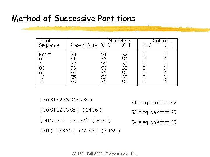
Algorithmic Approach to State Minimization z Goal – identify and combine states that have equivalent behavior z Equivalent States: y Same output y For all input combinations, states transition to same or equivalent states z Algorithm Sketch y 1. Place all states in one set y 2. Initially partition set based on output behavior y 3. Successively partition resulting subsets based on next state transitions y 4. Repeat (3) until no further partitioning is required xstates left in the same set are equivalent y Polynomial time procedure CS 150 - Fall 2000 - Introduction - 112

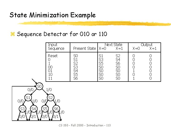
State Minimization Example z Sequence Detector for 010 or 110 0/0 S 3 0/0 S 1 1/0 S 0 0/0 S 4 S 5 0/1 Next State Present State X=0 X=1 Output X=0 X=1 Reset 0 1 00 01 10 11 S 0 S 1 S 2 S 3 S 4 S 5 S 6 0 0 1 0 1 S 3 S 5 S 0 S 0 1/0 1/0 Input Sequence 0/0 S 2 1/0 S 6 0/1 1/0 CS 150 - Fall 2000 - Introduction - 113 S 2 S 4 S 6 S 0 S 0 0 0 0 0

Method of Successive Partitions Input Sequence Next State Present State X=0 X=1 Output X=0 X=1 Reset 0 1 00 01 10 11 S 0 S 1 S 2 S 3 S 4 S 5 S 6 0 0 1 0 1 S 3 S 5 S 0 S 0 ( S 0 S 1 S 2 S 3 S 4 S 5 S 6 ) ( S 0 S 1 S 2 S 3 S 5 ) ( S 4 S 6 ) ( S 0 S 3 S 5 ) ( S 1 S 2 ) ( S 4 S 6 ) S 2 S 4 S 6 S 0 S 0 0 0 0 0 S 1 is equivalent to S 2 S 3 is equivalent to S 5 S 4 is equivalent to S 6 ( S 0 ) ( S 3 S 5 ) ( S 1 S 2 ) ( S 4 S 6 ) CS 150 - Fall 2000 - Introduction - 114

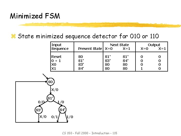
Minimized FSM z State minimized sequence detector for 010 or 110 Input Sequence Next State Present State X=0 X=1 Output X=0 X=1 Reset 0+1 X 0 X 1 S 0 S 1' S 3' S 4' 0 0 0 1 S 1' S 3' S 0 S 0 X/0 0/0 S 1’ 1/0 S 4’ S 3’ X/0 0/1 1/0 CS 150 - Fall 2000 - Introduction - 115 S 1' S 4' S 0 0 0

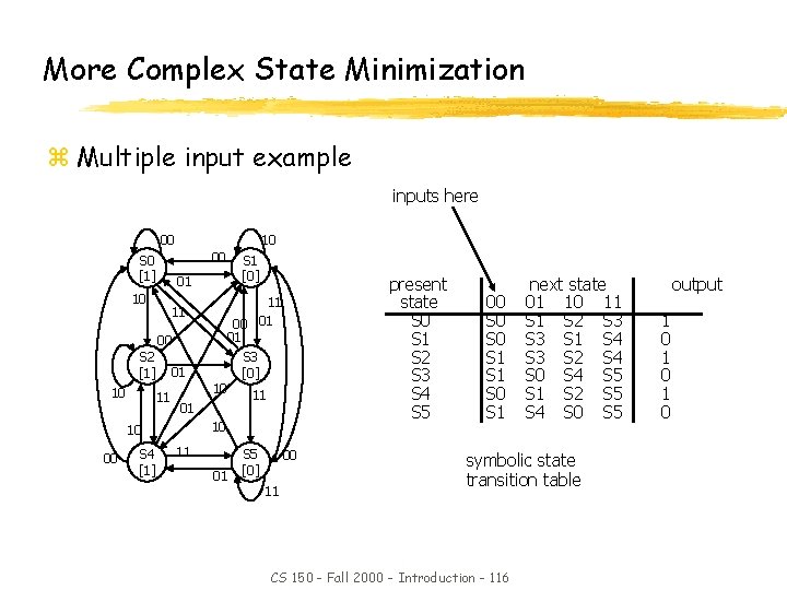
More Complex State Minimization z Multiple input example inputs here 00 10 00 S 0 [1] 01 10 S 2 [1] 01 11 10 01 S 4 [1] S 3 [0] 11 10 10 00 present state S 0 S 1 S 2 S 3 S 4 S 5 11 00 01 01 11 00 10 S 1 [0] 11 01 S 5 [0] 00 11 00 S 0 S 1 next state 01 10 11 S 2 S 3 S 1 S 4 S 3 S 2 S 4 S 0 S 4 S 5 S 1 S 2 S 5 S 4 S 0 S 5 symbolic state transition table CS 150 - Fall 2000 - Introduction - 116 output 1 0 1 0

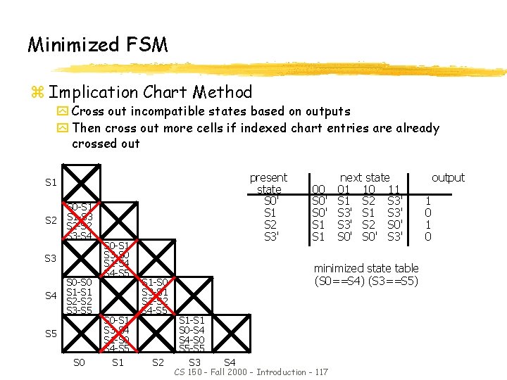
Minimized FSM z Implication Chart Method y Cross out incompatible states based on outputs y Then cross out more cells if indexed chart entries are already crossed out present state S 0' S 1 S 2 S 3' S 1 S 2 S 0 -S 1 S 1 -S 3 S 2 -S 2 S 3 -S 4 S 3 S 4 S 0 -S 0 S 1 -S 1 S 2 -S 2 S 3 -S 5 S 0 S 0 -S 1 S 3 -S 0 S 1 -S 4 S 4 -S 5 S 0 -S 1 S 3 -S 4 S 1 -S 0 S 4 -S 5 S 1 -S 0 S 3 -S 1 S 2 -S 2 S 4 -S 5 S 2 next state 00 01 10 11 S 0' S 1 S 2 S 3' S 0' S 3' S 1 S 3' S 2 S 0' S 1 S 0' S 3' minimized state table (S 0==S 4) (S 3==S 5) S 1 -S 1 S 0 -S 4 S 4 -S 0 S 5 -S 5 S 3 S 4 CS 150 - Fall 2000 - Introduction - 117 output 1 0

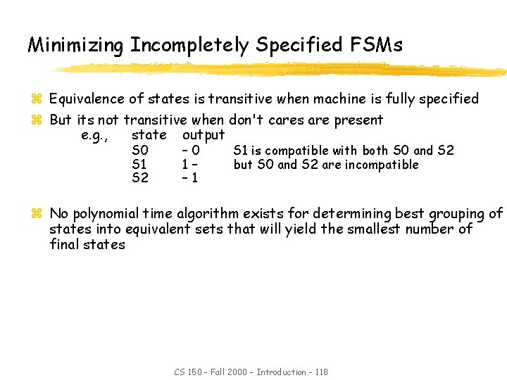
Minimizing Incompletely Specified FSMs z Equivalence of states is transitive when machine is fully specified z But its not transitive when don't cares are present e. g. , state output S 0 S 1 S 2 – 0 1– – 1 S 1 is compatible with both S 0 and S 2 but S 0 and S 2 are incompatible z No polynomial time algorithm exists for determining best grouping of states into equivalent sets that will yield the smallest number of final states CS 150 - Fall 2000 - Introduction - 118

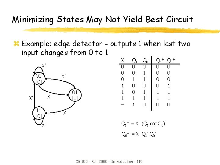
Minimizing States May Not Yield Best Circuit z Example: edge detector - outputs 1 when last two input changes from 0 to 1 X’ 00 [0] X’ 01 [1] X X’ 11 [0] X X 0 0 0 1 1 1 – Q 1 0 0 1 1 Q 0 0 1 1 0 Q 1+ 0 0 1 1 0 X Q 1+ = X (Q 1 xor Q 0) Q 0+ = X Q 1’ Q 0’ CS 150 - Fall 2000 - Introduction - 119 Q 0+ 0 0 0 1 1 1 0

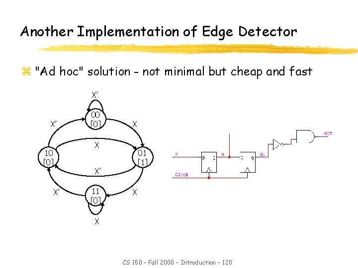
Another Implementation of Edge Detector z "Ad hoc" solution - not minimal but cheap and fast X’ X’ 10 [0] X’ 00 [0] X X’ 11 [0] X 01 [1] X X CS 150 - Fall 2000 - Introduction - 120

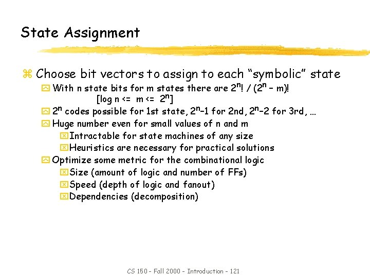
State Assignment z Choose bit vectors to assign to each “symbolic” state y With n state bits for m states there are 2 n! / (2 n – m)! [log n <= m <= 2 n] y 2 n codes possible for 1 st state, 2 n– 1 for 2 nd, 2 n– 2 for 3 rd, … y Huge number even for small values of n and m x. Intractable for state machines of any size x. Heuristics are necessary for practical solutions y Optimize some metric for the combinational logic x. Size (amount of logic and number of FFs) x. Speed (depth of logic and fanout) x. Dependencies (decomposition) CS 150 - Fall 2000 - Introduction - 121

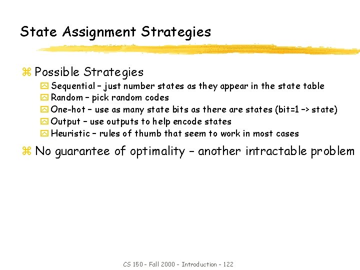
State Assignment Strategies z Possible Strategies y Sequential – just number states as they appear in the state table y Random – pick random codes y One-hot – use as many state bits as there are states (bit=1 –> state) y Output – use outputs to help encode states y Heuristic – rules of thumb that seem to work in most cases z No guarantee of optimality – another intractable problem CS 150 - Fall 2000 - Introduction - 122

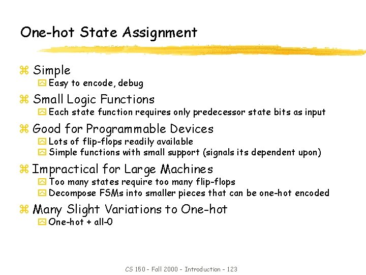
One-hot State Assignment z Simple y Easy to encode, debug z Small Logic Functions y Each state function requires only predecessor state bits as input z Good for Programmable Devices y Lots of flip-flops readily available y Simple functions with small support (signals its dependent upon) z Impractical for Large Machines y Too many states require too many flip-flops y Decompose FSMs into smaller pieces that can be one-hot encoded z Many Slight Variations to One-hot y One-hot + all-0 CS 150 - Fall 2000 - Introduction - 123

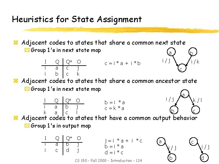
Heuristics for State Assignment z Adjacent codes to states that share a common next state y Group 1's in next state map I i i Q a b Q+ c c O j k a b i/j c=i*a + i*b i/k c z Adjacent codes to states that share a common ancestor state y Group 1's in next state map I i k Q a a Q+ b c O j l i/j b=i *a c=k*a b a k/l c z Adjacent codes to states that have a common output behavior y Group 1's in output map I i i Q a c Q+ b d O j j j=i *a+ i *c b=i*a d=i*c CS 150 - Fall 2000 - Introduction - 124 a c i/j b d

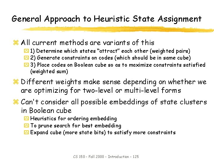
General Approach to Heuristic State Assignment z All current methods are variants of this y 1) Determine which states “attract” each other (weighted pairs) y 2) Generate constraints on codes (which should be in same cube) y 3) Place codes on Boolean cube so as to maximize constraints satisfied (weighted sum) z Different weights make sense depending on whether we are optimizing for two-level or multi-level forms z Can't consider all possible embeddings of state clusters in Boolean cube y Heuristics for ordering embedding y To prune search for best embedding y Expand cube (more state bits) to satisfy more constraints CS 150 - Fall 2000 - Introduction - 125

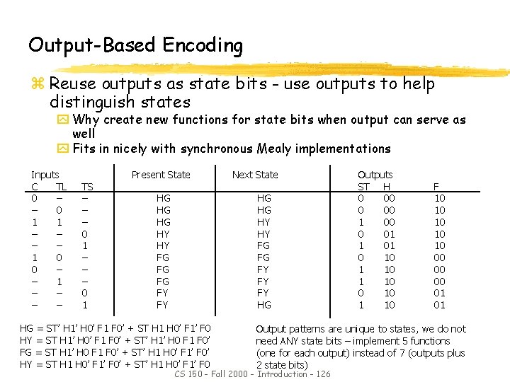
Output-Based Encoding z Reuse outputs as state bits - use outputs to help distinguish states y Why create new functions for state bits when output can serve as well y Fits in nicely with synchronous Mealy implementations Inputs C TL 0 – – 0 1 1 – – 1 0 0 – – 1 – – TS – – – 0 1 Present State HG HG HG HY HY FG FG FG FY FY Next State HG HG HY HY FG FG FY FY FY HG HG = ST’ H 1’ H 0’ F 1 F 0’ + ST H 1 H 0’ F 1’ F 0 HY = ST H 1’ H 0’ F 1 F 0’ + ST’ H 1’ H 0 F 1 F 0’ FG = ST H 1’ H 0 F 1 F 0’ + ST’ H 1 H 0’ F 1’ F 0’ HY = ST H 1 H 0’ F 1’ F 0’ + ST’ H 1 H 0’ F 1’ F 0 Outputs ST H 0 00 1 00 0 01 1 01 0 10 1 10 F 10 10 10 00 01 01 Output patterns are unique to states, we do not need ANY state bits – implement 5 functions (one for each output) instead of 7 (outputs plus 2 state bits) CS 150 - Fall 2000 - Introduction - 126

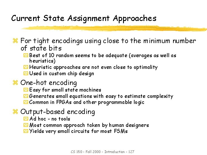
Current State Assignment Approaches z For tight encodings using close to the minimum number of state bits y Best of 10 random seems to be adequate (averages as well as heuristics) y Heuristic approaches are not even close to optimality y Used in custom chip design z One-hot encoding y Easy for small state machines y Generates small equations with easy to estimate complexity y Common in FPGAs and other programmable logic z Output-based encoding y Ad hoc - no tools y Most common approach taken by human designers y Yields very small circuits for most FSMs CS 150 - Fall 2000 - Introduction - 127

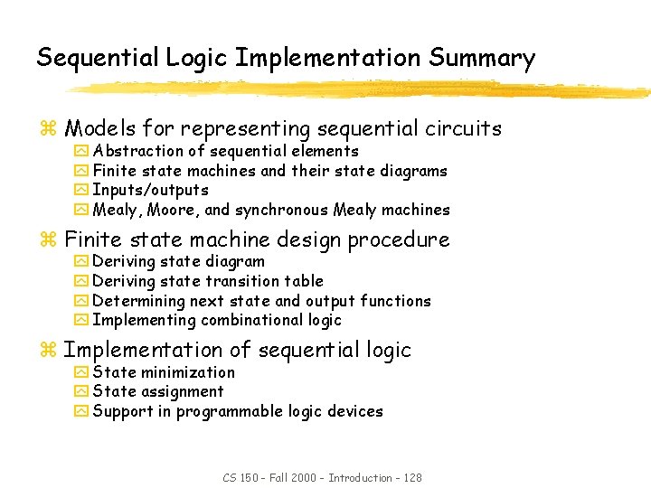
Sequential Logic Implementation Summary z Models for representing sequential circuits y Abstraction of sequential elements y Finite state machines and their state diagrams y Inputs/outputs y Mealy, Moore, and synchronous Mealy machines z Finite state machine design procedure y Deriving state diagram y Deriving state transition table y Determining next state and output functions y Implementing combinational logic z Implementation of sequential logic y State minimization y State assignment y Support in programmable logic devices CS 150 - Fall 2000 - Introduction - 128

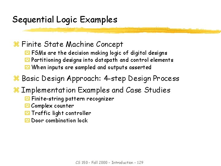
Sequential Logic Examples z Finite State Machine Concept y FSMs are the decision making logic of digital designs y Partitioning designs into datapath and control elements y When inputs are sampled and outputs asserted z Basic Design Approach: 4 -step Design Process z Implementation Examples and Case Studies y Finite-string pattern recognizer y Complex counter y Traffic light controller y Door combination lock CS 150 - Fall 2000 - Introduction - 129

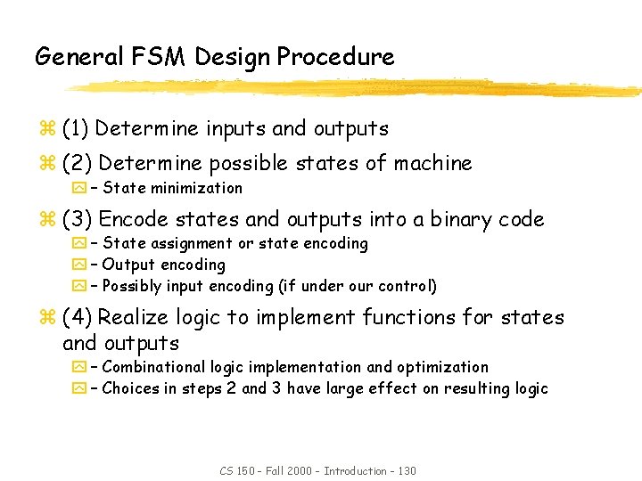
General FSM Design Procedure z (1) Determine inputs and outputs z (2) Determine possible states of machine y – State minimization z (3) Encode states and outputs into a binary code y – State assignment or state encoding y – Output encoding y – Possibly input encoding (if under our control) z (4) Realize logic to implement functions for states and outputs y – Combinational logic implementation and optimization y – Choices in steps 2 and 3 have large effect on resulting logic CS 150 - Fall 2000 - Introduction - 130

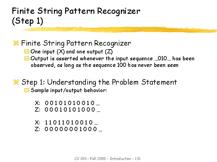
Finite String Pattern Recognizer (Step 1) z Finite String Pattern Recognizer y One input (X) and one output (Z) y Output is asserted whenever the input sequence … 010… has been observed, as long as the sequence 100 has never been seen z Step 1: Understanding the Problem Statement y Sample input/output behavior: X: 0 0 1 0 1 0 … Z: 0 0 0 1 0 1 0 0 0 … X: 1 1 0 1 0 … Z: 0 0 0 0 1 0 0 0 … CS 150 - Fall 2000 - Introduction - 131

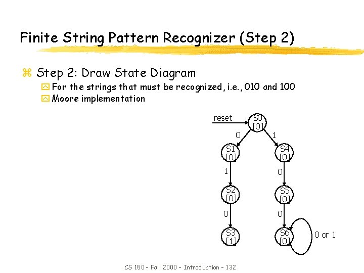
Finite String Pattern Recognizer (Step 2) z Step 2: Draw State Diagram y For the strings that must be recognized, i. e. , 010 and 100 y Moore implementation reset 0 S 0 [0] 1 S 1 [0] S 4 [0] 1 0 S 2 [0] S 5 [0] 0 0 S 3 [1] S 6 [0] CS 150 - Fall 2000 - Introduction - 132 0 or 1

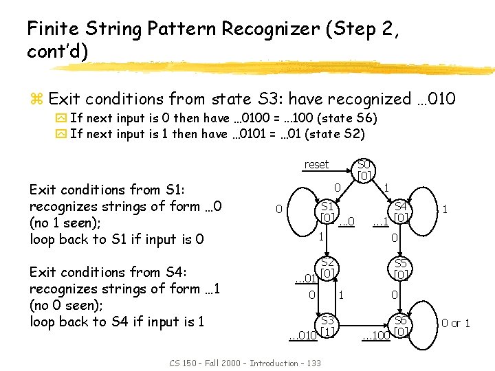
Finite String Pattern Recognizer (Step 2, cont’d) z Exit conditions from state S 3: have recognized … 010 y If next input is 0 then have … 0100 =. . . 100 (state S 6) y If next input is 1 then have … 0101 = … 01 (state S 2) reset Exit conditions from S 1: recognizes strings of form … 0 (no 1 seen); loop back to S 1 if input is 0 Exit conditions from S 4: recognizes strings of form … 1 (no 0 seen); loop back to S 4 if input is 1 0 0 S 1 [0]. . . 0 1 S 2. . . 01 [0] 0 1 S 3. . . 010 [1] CS 150 - Fall 2000 - Introduction - 133 S 0 [0] 1 S 4. . . 1 [0] 0 1 S 5 [0] 0 S 6. . . 100 [0] 0 or 1

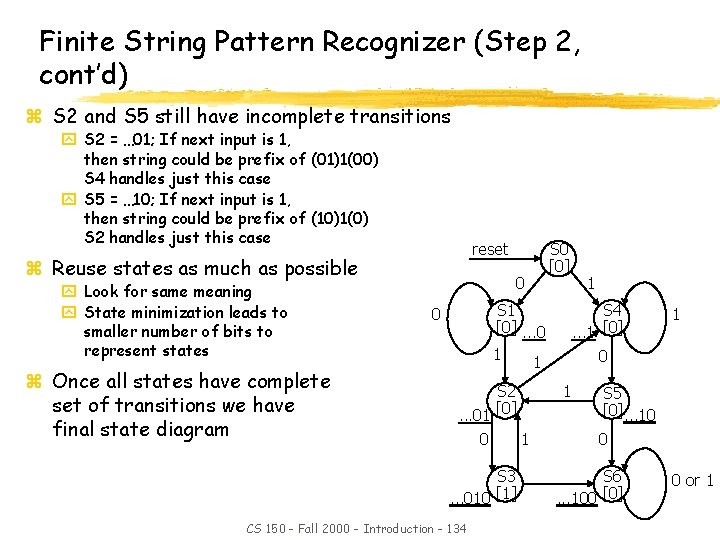
Finite String Pattern Recognizer (Step 2, cont’d) z S 2 and S 5 still have incomplete transitions y S 2 = … 01; If next input is 1, then string could be prefix of (01)1(00) S 4 handles just this case y S 5 = … 10; If next input is 1, then string could be prefix of (10)1(0) S 2 handles just this case reset z Reuse states as much as possible y Look for same meaning y State minimization leads to smaller number of bits to represent states z Once all states have complete set of transitions we have final state diagram 0 S 0 [0] S 1 [0]. . . 0 1 1 0 S 2. . . 01 [0] 0 1 S 3. . . 010 [1] CS 150 - Fall 2000 - Introduction - 134 1 S 4. . . 1 [0] 0 1 1 S 5 [0]. . . 10 0 S 6. . . 100 [0] 0 or 1

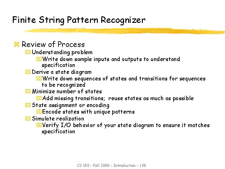
Finite String Pattern Recognizer z Review of Process y Understanding problem x. Write down sample inputs and outputs to understand specification y Derive a state diagram x. Write down sequences of states and transitions for sequences to be recognized y Minimize number of states x. Add missing transitions; reuse states as much as possible y State assignment or encoding x. Encode states with unique patterns y Simulate realization x. Verify I/O behavior of your state diagram to ensure it matches specification CS 150 - Fall 2000 - Introduction - 135

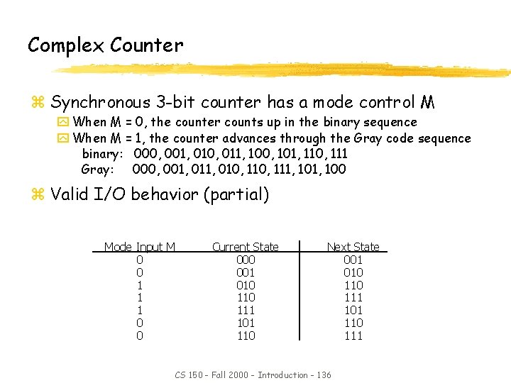
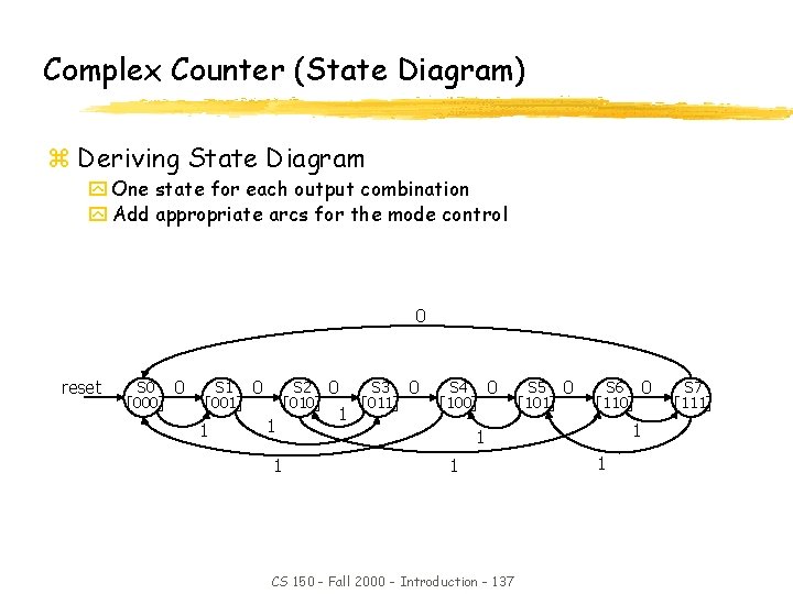
Complex Counter z Synchronous 3 -bit counter has a mode control M y When M = 0, the counter counts up in the binary sequence y When M = 1, the counter advances through the Gray code sequence binary: 000, 001, 010, 011, 100, 101, 110, 111 Gray: 000, 001, 010, 111, 100 z Valid I/O behavior (partial) Mode Input M 0 0 1 1 1 0 0 Current State 000 001 010 111 101 110 Next State 001 010 111 101 110 111 CS 150 - Fall 2000 - Introduction - 136

Complex Counter (State Diagram) z Deriving State Diagram y One state for each output combination y Add appropriate arcs for the mode control 0 reset S 0 0 [000] S 1 0 [001] 1 S 2 0 [010] 1 1 1 S 3 0 [011] S 4 0 [100] S 5 0 [101] S 6 0 [110] 1 1 1 CS 150 - Fall 2000 - Introduction - 137 1 S 7 [111]

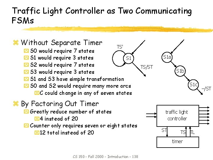
Traffic Light Controller as Two Communicating FSMs z Without Separate Timer TS' y S 0 would require 7 states y S 1 would require 3 states S 1 y S 2 would require 7 states y S 3 would require 3 states y S 1 and S 3 have simple transformation y S 0 and S 2 would require many more arcs x. C could change in any of seven states S 1 a TS/ST S 1 b S 1 c z By Factoring Out Timer y Greatly reduce number of states x 4 instead of 20 y Counter only requires seven or eight states x 12 total instead of 20 traffic light controller ST TS TL timer CS 150 - Fall 2000 - Introduction - 138 –/ST

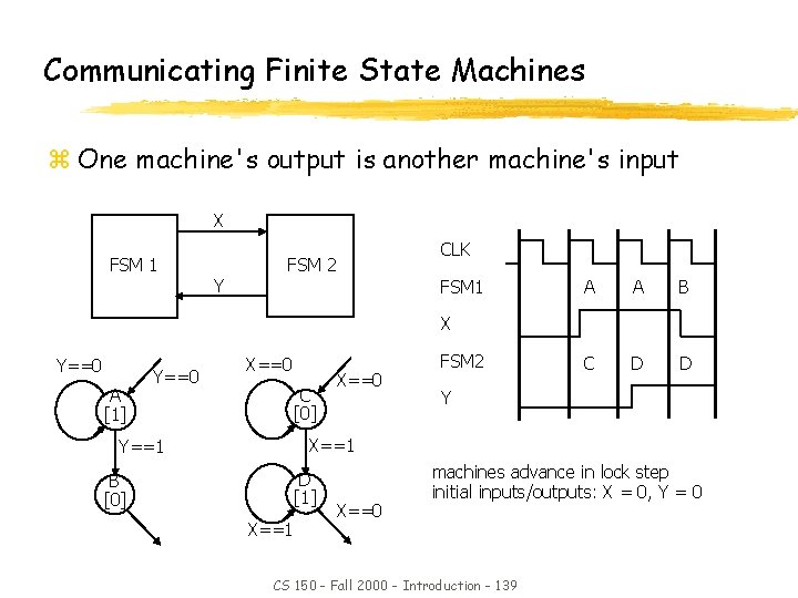
Communicating Finite State Machines z One machine's output is another machine's input X FSM 1 Y CLK FSM 2 FSM 1 A A B C D D X Y==0 A [1] Y==0 X==0 C [0] Y X==1 Y==1 B [0] X==0 FSM 2 D [1] X==1 X==0 machines advance in lock step initial inputs/outputs: X = 0, Y = 0 CS 150 - Fall 2000 - Introduction - 139

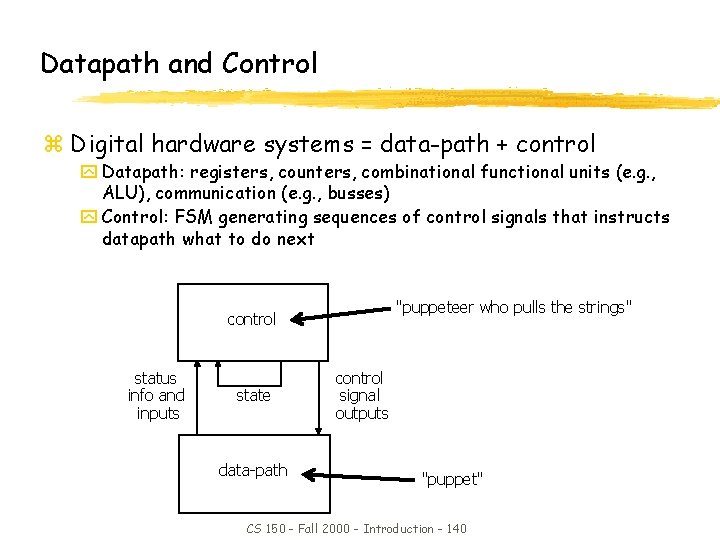
Datapath and Control z Digital hardware systems = data-path + control y Datapath: registers, counters, combinational functional units (e. g. , ALU), communication (e. g. , busses) y Control: FSM generating sequences of control signals that instructs datapath what to do next "puppeteer who pulls the strings" control status info and inputs state data-path control signal outputs "puppet" CS 150 - Fall 2000 - Introduction - 140

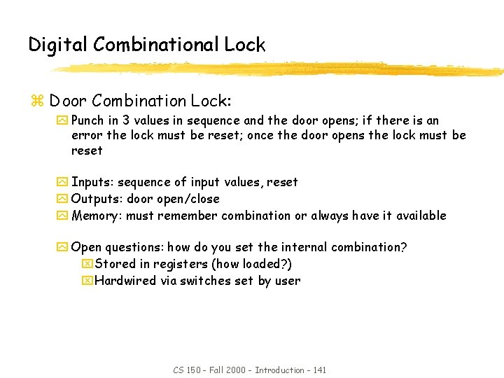
Digital Combinational Lock z Door Combination Lock: y Punch in 3 values in sequence and the door opens; if there is an error the lock must be reset; once the door opens the lock must be reset y Inputs: sequence of input values, reset y Outputs: door open/close y Memory: must remember combination or always have it available y Open questions: how do you set the internal combination? x. Stored in registers (how loaded? ) x. Hardwired via switches set by user CS 150 - Fall 2000 - Introduction - 141

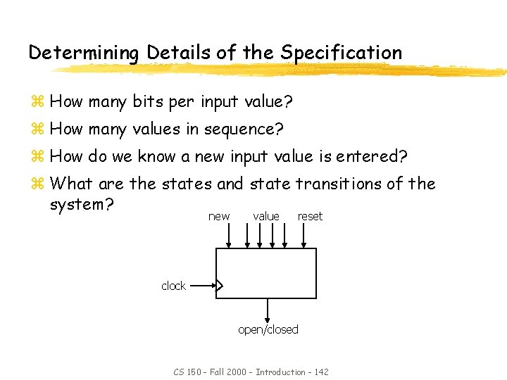
Determining Details of the Specification z How many bits per input value? z How many values in sequence? z How do we know a new input value is entered? z What are the states and state transitions of the system? new value reset clock open/closed CS 150 - Fall 2000 - Introduction - 142

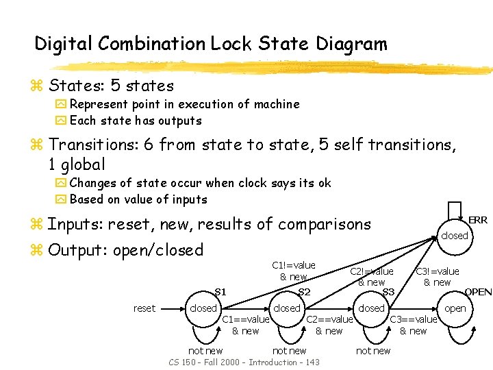
Digital Combination Lock State Diagram z States: 5 states y Represent point in execution of machine y Each state has outputs z Transitions: 6 from state to state, 5 self transitions, 1 global y Changes of state occur when clock says its ok y Based on value of inputs z Inputs: reset, new, results of comparisons z Output: open/closed C 1!=value & new S 1 reset closed C 1==value & new not new S 2 closed CS 150 - Fall 2000 - Introduction - 143 closed C 2!=value & new S 3 C 2==value & new not new ERR closed C 3!=value & new C 3==value & new not new OPEN open

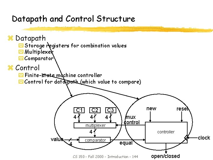
Datapath and Control Structure z Datapath y Storage registers for combination values y Multiplexer y Comparator z Control y Finite-state machine controller y Control for data-path (which value to compare) C 1 4 C 2 4 C 3 4 multiplexer new mux control 4 value 4 comparator reset controller clock equal CS 150 - Fall 2000 - Introduction - 144 open/closed

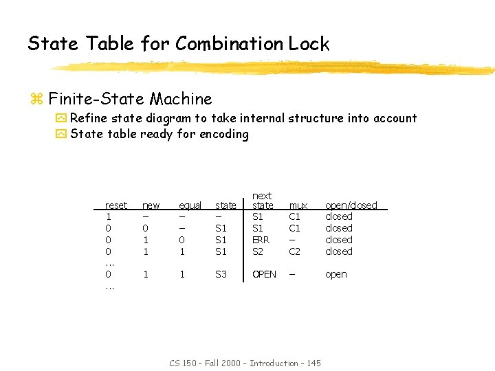
State Table for Combination Lock z Finite-State Machine y Refine state diagram to take internal structure into account y State table ready for encoding reset 1 0 0 0. . . new – 0 1 1 equal – – 0 1 state – S 1 S 1 next state S 1 ERR S 2 mux C 1 – C 2 open/closed closed 1 1 S 3 OPEN – open CS 150 - Fall 2000 - Introduction - 145

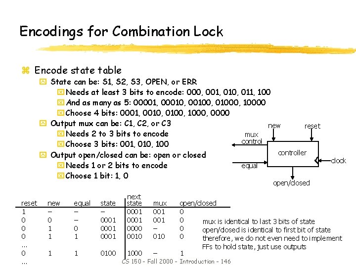
Encodings for Combination Lock z Encode state table y State can be: S 1, S 2, S 3, OPEN, or ERR x Needs at least 3 bits to encode: 000, 001, 010, 011, 100 x And as many as 5: 00001, 00010, 00100, 01000, 10000 x Choose 4 bits: 0001, 0010, 0100, 1000, 0000 y Output mux can be: C 1, C 2, or C 3 new reset x Needs 2 to 3 bits to encode mux control x Choose 3 bits: 001, 010, 100 controller y Output open/closed can be: open or closed x Needs 1 or 2 bits to encode equal x Choose 1 bit: 1, 0 clock open/closed reset 1 0 0 0. . . new – 0 1 1 equal – – 0 1 state – 0001 next state 0001 0000 0010 1 1 0100 1000 mux 001 – 010 – open/closed 0 0 mux is identical to last 3 bits of state 0 open/closed is identical to first bit of state 0 therefore, we do not even need to implement FFs to hold state, just use outputs 1 CS 150 - Fall 2000 - Introduction - 146

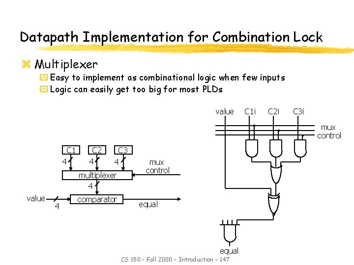
Datapath Implementation for Combination Lock z Multiplexer y Easy to implement as combinational logic when few inputs y Logic can easily get too big for most PLDs value C 1 i C 2 i C 3 i mux control C 1 4 C 2 4 C 3 4 multiplexer 4 value 4 comparator mux control equal CS 150 - Fall 2000 - Introduction - 147

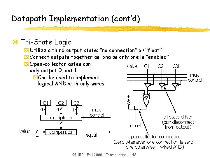
Datapath Implementation (cont’d) z Tri-State Logic y Utilize a third output state: “no connection” or “float” y Connect outputs together as long as only one is “enabled” y Open-collector gates can value C 1 i C 2 i C 3 i only output 0, not 1 x. Can be used to implement logical AND with only wires + C 1 4 C 2 4 C 3 4 multiplexer 4 value 4 comparator mux control equal mux control oc tri-state driver (can disconnect from output) open-collector connection (zero whenever one connection is zero, one otherwise – wired AND) CS 150 - Fall 2000 - Introduction - 148

Tri-states z Very important in real life z Probably not as important on the test… z You should know how they work by now anyways. CS 150 - Fall 2000 - Introduction - 149

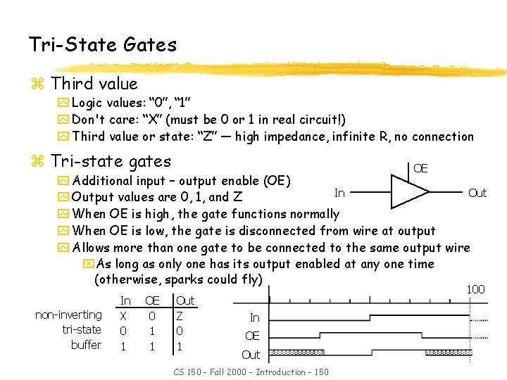
Tri-State Gates z Third value y Logic values: “ 0”, “ 1” y Don't care: “X” (must be 0 or 1 in real circuit!) y Third value or state: “Z” — high impedance, infinite R, no connection z Tri-state gates OE y Additional input – output enable (OE) In Out y Output values are 0, 1, and Z y When OE is high, the gate functions normally y When OE is low, the gate is disconnected from wire at output y Allows more than one gate to be connected to the same output wire x. As long as only one has its output enabled at any one time (otherwise, sparks could fly) non-inverting tri-state buffer In X 0 1 OE 0 1 1 Out Z 0 1 100 In OE Out CS 150 - Fall 2000 - Introduction - 150

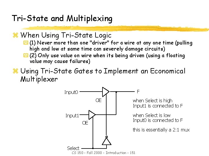
Tri-State and Multiplexing z When Using Tri-State Logic y (1) Never more than one "driver" for a wire at any one time (pulling high and low at same time can severely damage circuits) y (2) Only use value on wire when its being driven (using a floating value may cause failures) z Using Tri-State Gates to Implement an Economical Multiplexer F Input 0 OE Input 1 OE when Select is high Input 1 is connected to F when Select is low Input 0 is connected to F this is essentially a 2: 1 mux Select CS 150 - Fall 2000 - Introduction - 151

Open-Collector Gates and Wired-AND z Um… I didn’t know what they were, and had to ask prof. Katz after class z Not too important. CS 150 - Fall 2000 - Introduction - 152

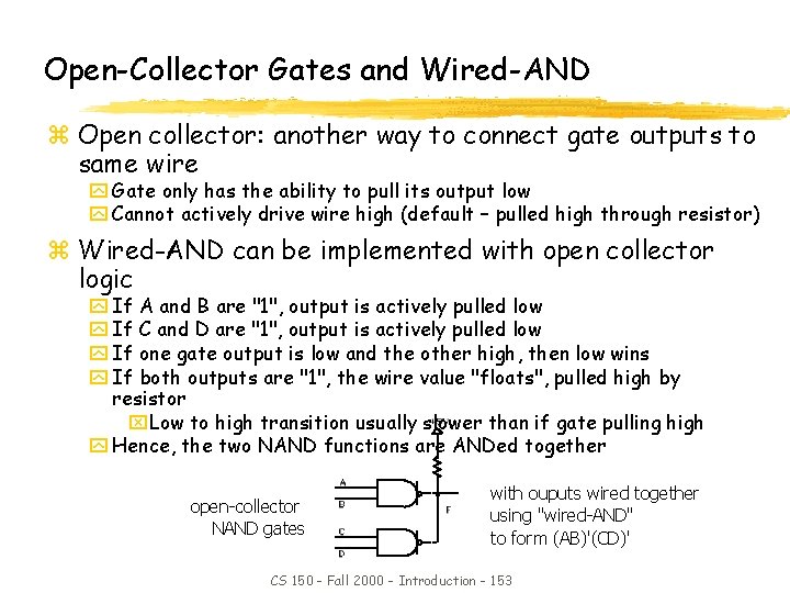
Open-Collector Gates and Wired-AND z Open collector: another way to connect gate outputs to same wire y Gate only has the ability to pull its output low y Cannot actively drive wire high (default – pulled high through resistor) z Wired-AND can be implemented with open collector logic y If A and B are "1", output is actively pulled low y If C and D are "1", output is actively pulled low y If one gate output is low and the other high, then low wins y If both outputs are "1", the wire value "floats", pulled high by resistor x. Low to high transition usually slower than if gate pulling high y Hence, the two NAND functions are ANDed together open-collector NAND gates with ouputs wired together using "wired-AND" to form (AB)'(CD)' CS 150 - Fall 2000 - Introduction - 153

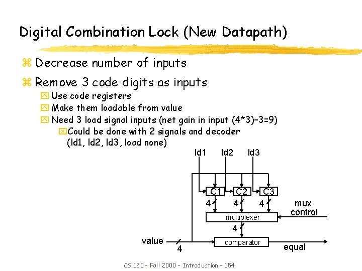
Digital Combination Lock (New Datapath) z Decrease number of inputs z Remove 3 code digits as inputs y Use code registers y Make them loadable from value y Need 3 load signal inputs (net gain in input (4*3)– 3=9) x. Could be done with 2 signals and decoder (ld 1, ld 2, ld 3, load none) ld 1 ld 2 ld 3 C 1 4 C 2 4 C 3 4 multiplexer mux control 4 value 4 comparator CS 150 - Fall 2000 - Introduction - 154 equal

Section Summary z FSM Design y Understanding the problem y Generating state diagram y Implementation using synthesis tools y Iteration on design/specification to improve qualities of mapping y Communicating state machines z Four case studies y Understand I/O behavior y Draw diagrams y Enumerate states for the "goal" y Expand with error conditions y Reuse states whenever possible CS 150 - Fall 2000 - Introduction - 155

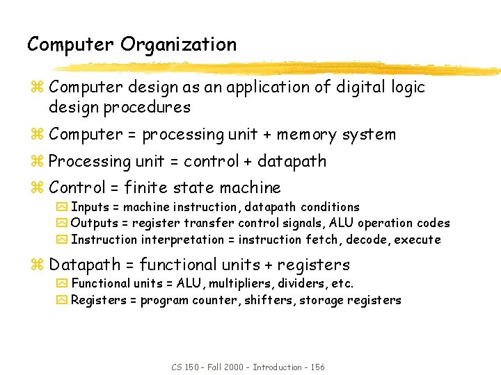
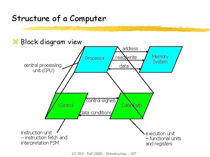
Computer Organization z Computer design as an application of digital logic design procedures z Computer = processing unit + memory system z Processing unit = control + datapath z Control = finite state machine y Inputs = machine instruction, datapath conditions y Outputs = register transfer control signals, ALU operation codes y Instruction interpretation = instruction fetch, decode, execute z Datapath = functional units + registers y Functional units = ALU, multipliers, dividers, etc. y Registers = program counter, shifters, storage registers CS 150 - Fall 2000 - Introduction - 156

Structure of a Computer z Block diagram view address Processor read/write central processing unit (CPU) data Control control signals Memory System Data Path data conditions instruction unit – instruction fetch and interpretation FSM execution unit – functional units and registers CS 150 - Fall 2000 - Introduction - 157

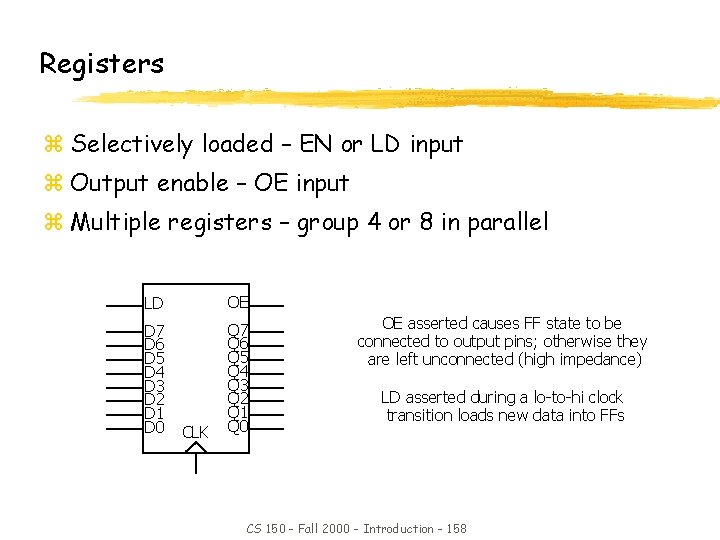
Registers z Selectively loaded – EN or LD input z Output enable – OE input z Multiple registers – group 4 or 8 in parallel LD OE D 7 D 6 D 5 D 4 D 3 D 2 D 1 D 0 Q 7 Q 6 Q 5 Q 4 Q 3 Q 2 Q 1 Q 0 CLK OE asserted causes FF state to be connected to output pins; otherwise they are left unconnected (high impedance) LD asserted during a lo-to-hi clock transition loads new data into FFs CS 150 - Fall 2000 - Introduction - 158

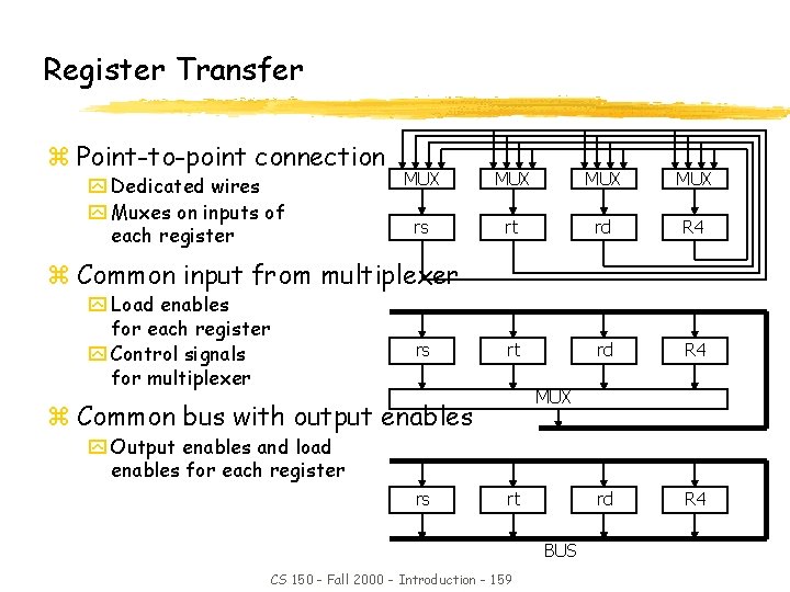
Register Transfer z Point-to-point connection y Dedicated wires y Muxes on inputs of each register MUX MUX rs rt rd R 4 z Common input from multiplexer y Load enables for each register y Control signals for multiplexer rs MUX z Common bus with output enables y Output enables and load enables for each register rs rt BUS CS 150 - Fall 2000 - Introduction - 159

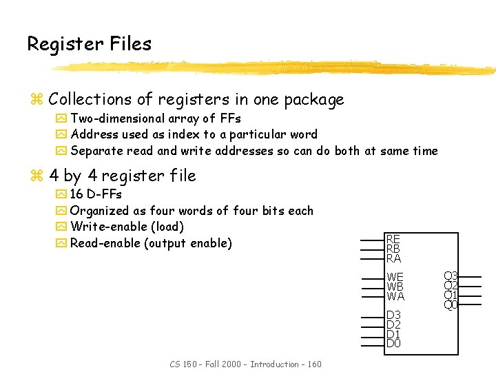
Register Files z Collections of registers in one package y Two-dimensional array of FFs y Address used as index to a particular word y Separate read and write addresses so can do both at same time z 4 by 4 register file y 16 D-FFs y Organized as four words of four bits each y Write-enable (load) y Read-enable (output enable) RE RB RA WE WB WA D 3 D 2 D 1 D 0 CS 150 - Fall 2000 - Introduction - 160 Q 3 Q 2 Q 1 Q 0

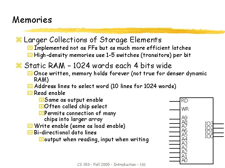
Memories z Larger Collections of Storage Elements y Implemented not as FFs but as much more efficient latches y High-density memories use 1 -5 switches (transitors) per bit z Static RAM – 1024 words each 4 bits wide y Once written, memory holds forever (not true for denser dynamic RAM) y Address lines to select word (10 lines for 1024 words) y Read enable x. Same as output enable RD x. Often called chip select WR x. Permits connection of many A 9 chips into larger array A 8 IO 3 y Write enable (same as load enable) A 7 IO 2 A 6 IO 1 y Bi-directional data lines A 5 IO 0 A 4 xoutput when reading, input when writing CS 150 - Fall 2000 - Introduction - 161 A 3 A 2 A 1 A 0

The rest is probably not too important for the test z Although it is a cool topic z Computer Architecture is fun, really z Make sure you understand the REGISTER FILE and MEMORY form the few slides before this one though. CS 150 - Fall 2000 - Introduction - 162

Instruction Sequencing z Example – an instruction to add the contents of two registers (Rx and Ry) and place result in a third register (Rz) z Step 1: Get the ADD instruction from memory into an instruction register z Step 2: Decode instruction y Instruction in IR has the code of an ADD instruction y Register indices used to generate output enables for registers Rx and Ry y Register index used to generate load signal for register Rz z Step 3: execute instruction y Enable Rx and Ry output and direct to ALU y Setup ALU to perform ADD operation y Direct result to Rz so that it can be loaded into register CS 150 - Fall 2000 - Introduction - 163

Instruction Types z Data Manipulation y Add, subtract y Increment, decrement y Multiply y Shift, rotate y Immediate operands z Data Staging y Load/store data to/from memory y Register-to-register move z Control y Conditional/unconditional branches in program flow y Subroutine call and return CS 150 - Fall 2000 - Introduction - 164

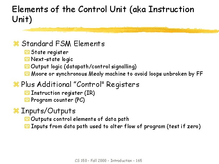
Elements of the Control Unit (aka Instruction Unit) z Standard FSM Elements y State register y Next-state logic y Output logic (datapath/control signalling) y Moore or synchronous Mealy machine to avoid loops unbroken by FF z Plus Additional ”Control" Registers y Instruction register (IR) y Program counter (PC) z Inputs/Outputs y Outputs control elements of data path y Inputs from data path used to alter flow of program (test if zero) CS 150 - Fall 2000 - Introduction - 165

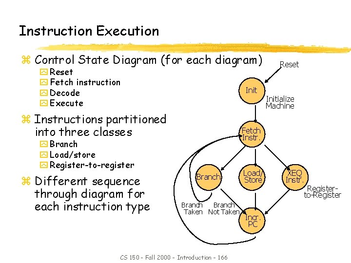
Instruction Execution z Control State Diagram (for each diagram) y Reset y Fetch instruction y Decode y Execute Init z Instructions partitioned into three classes Initialize Machine Fetch Instr. y Branch y Load/store y Register-to-register z Different sequence through diagram for each instruction type Reset Branch Taken Not Taken CS 150 - Fall 2000 - Introduction - 166 Load/ Store Incr. PC XEQ Instr. Registerto-Register

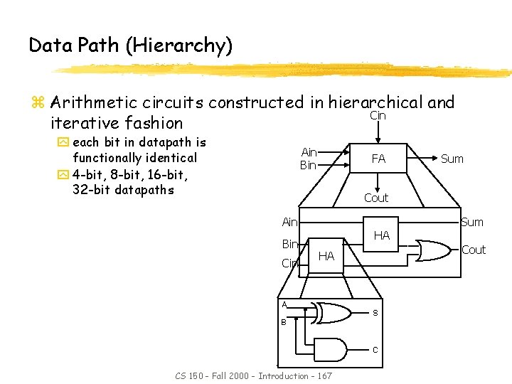
Data Path (Hierarchy) z Arithmetic circuits constructed in hierarchical and Cin iterative fashion y each bit in datapath is functionally identical y 4 -bit, 8 -bit, 16 -bit, 32 -bit datapaths Ain Bin FA Sum Cout Ain Bin Cin HA HA CS 150 - Fall 2000 - Introduction - 167 Sum Cout

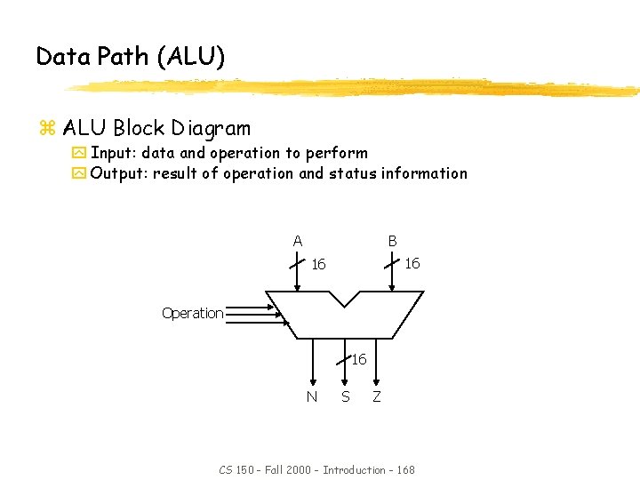
Data Path (ALU) z ALU Block Diagram y Input: data and operation to perform y Output: result of operation and status information A B 16 16 Operation 16 N S Z CS 150 - Fall 2000 - Introduction - 168

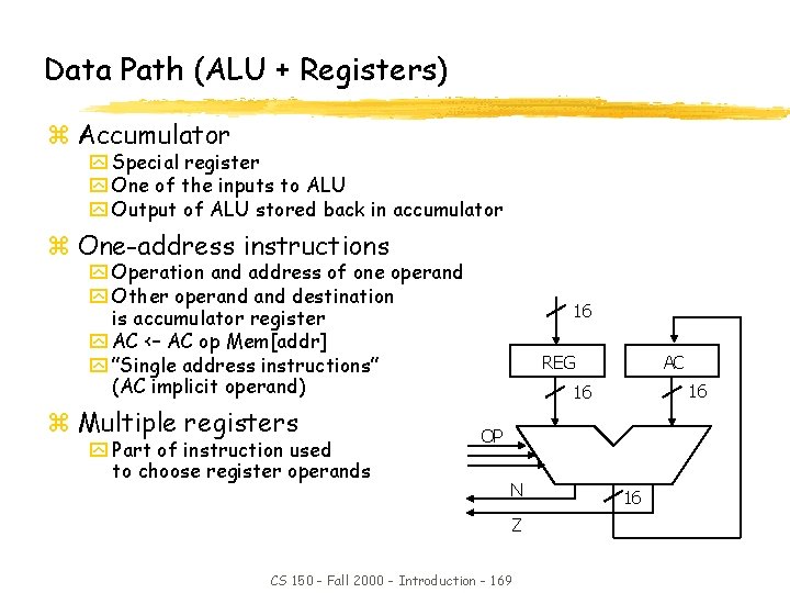
Data Path (ALU + Registers) z Accumulator y Special register y One of the inputs to ALU y Output of ALU stored back in accumulator z One-address instructions y Operation and address of one operand y Other operand destination is accumulator register y AC <– AC op Mem[addr] y ”Single address instructions” (AC implicit operand) z Multiple registers y Part of instruction used to choose register operands 16 REG AC 16 16 OP N Z CS 150 - Fall 2000 - Introduction - 169 16

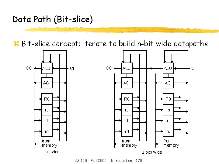
Data Path (Bit-slice) z Bit-slice concept: iterate to build n-bit wide datapaths CO ALU ALU AC AC AC R 0 R 0 rs rs rs rt rt rt rd rd rd from memory 1 bit wide CI from memory 2 bits wide CS 150 - Fall 2000 - Introduction - 170 CI

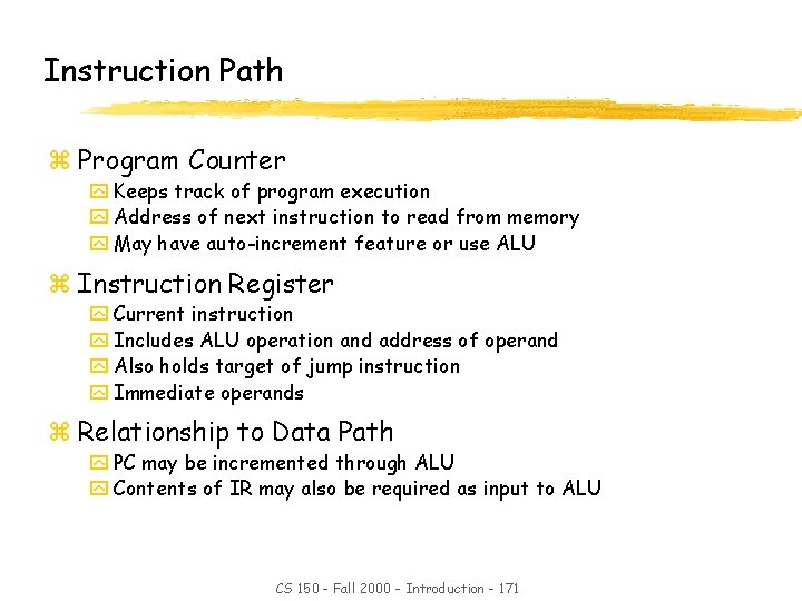
Instruction Path z Program Counter y Keeps track of program execution y Address of next instruction to read from memory y May have auto-increment feature or use ALU z Instruction Register y Current instruction y Includes ALU operation and address of operand y Also holds target of jump instruction y Immediate operands z Relationship to Data Path y PC may be incremented through ALU y Contents of IR may also be required as input to ALU CS 150 - Fall 2000 - Introduction - 171

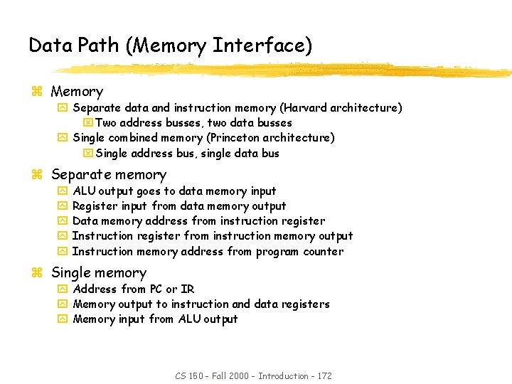
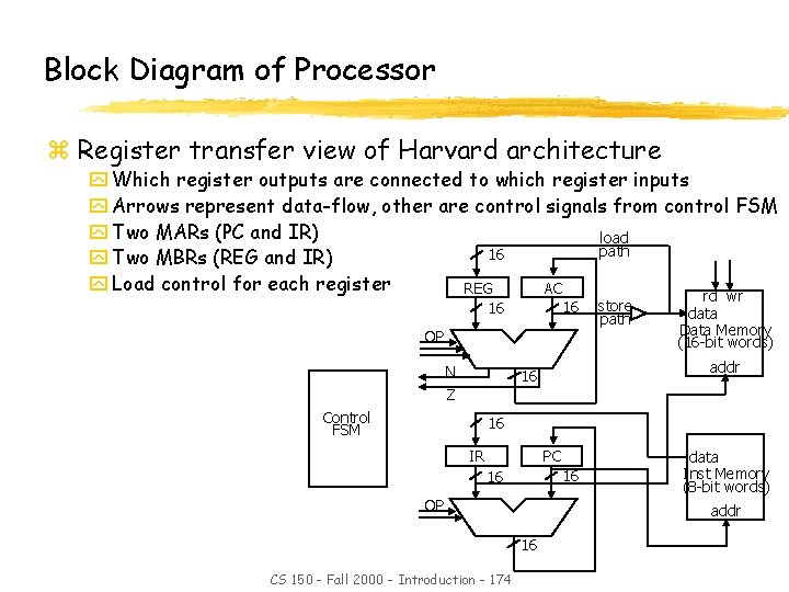
Data Path (Memory Interface) z Memory y Separate data and instruction memory (Harvard architecture) x Two address busses, two data busses y Single combined memory (Princeton architecture) x Single address bus, single data bus z Separate memory y y ALU output goes to data memory input Register input from data memory output Data memory address from instruction register Instruction register from instruction memory output Instruction memory address from program counter z Single memory y Address from PC or IR y Memory output to instruction and data registers y Memory input from ALU output CS 150 - Fall 2000 - Introduction - 172

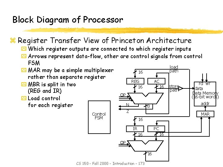
Block Diagram of Processor z Register Transfer View of Princeton Architecture y Which register outputs are connected to which register inputs y Arrows represent data-flow, other are control signals from control FSM load y MAR may be a simple multiplexer path 16 rather than separate register REG AC rd wr y MBR is split in two 16 store 16 data path (REG and IR) Data Memory OP (16 -bit words) y Load control addr N for each register 8 Z Control FSM MAR 16 IR PC 16 16 OP 16 CS 150 - Fall 2000 - Introduction - 173

Block Diagram of Processor z Register transfer view of Harvard architecture y Which register outputs are connected to which register inputs y Arrows represent data-flow, other are control signals from control FSM y Two MARs (PC and IR) load path 16 y Two MBRs (REG and IR) y Load control for each register REG AC 16 16 OP N Z rd wr data Data Memory (16 -bit words) addr 16 Control FSM store path 16 IR PC 16 16 OP addr 16 CS 150 - Fall 2000 - Introduction - 174 data Inst Memory (8 -bit words)

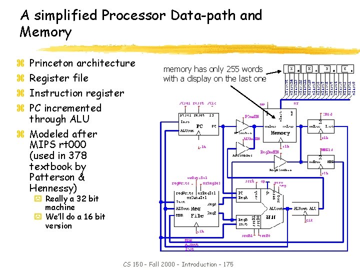
A simplified Processor Data-path and Memory z z Princeton architecture Register file Instruction register PC incremented through ALU z Modeled after MIPS rt 000 (used in 378 textbook by Patterson & Hennessy) memory has only 255 words with a display on the last one y Really a 32 bit machine y We’ll do a 16 bit version CS 150 - Fall 2000 - Introduction - 175

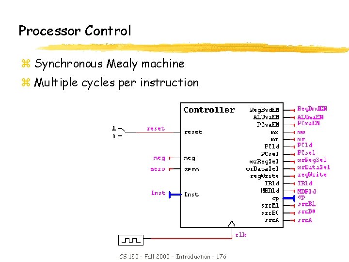
Processor Control z Synchronous Mealy machine z Multiple cycles per instruction CS 150 - Fall 2000 - Introduction - 176

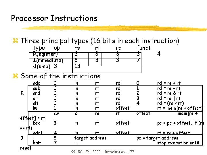
Processor Instructions z Three principal types (16 bits in each instruction) type op R(egister) I(mmediate) J(ump) 3 rs 3 3 13 rt 3 3 z Some of the instructions R add sub and or slt lw offset] = rt I beq == rt) addi j J halt reset rd 3 3 funct 3 7 0 1 2 3 4 0 0 0 1 sw rs rs rs 2 rt rt rt rs rd rd rd offset rt 3 rs rt offset 4 5 7 rs rt target address - offset CS 150 - Fall 2000 - Introduction - 177 offset 4 rd = rs + rt rd = rs - rt rd = rs & rt rd = rs | rt rd = (rs < rt) rt = mem[rs + offset] mem[rs + pc = pc + offset, if (rs rt = rs + offset pc = target address stop execution until

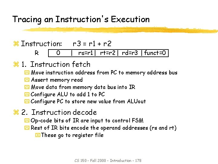
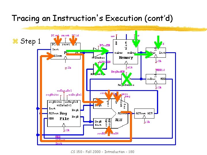
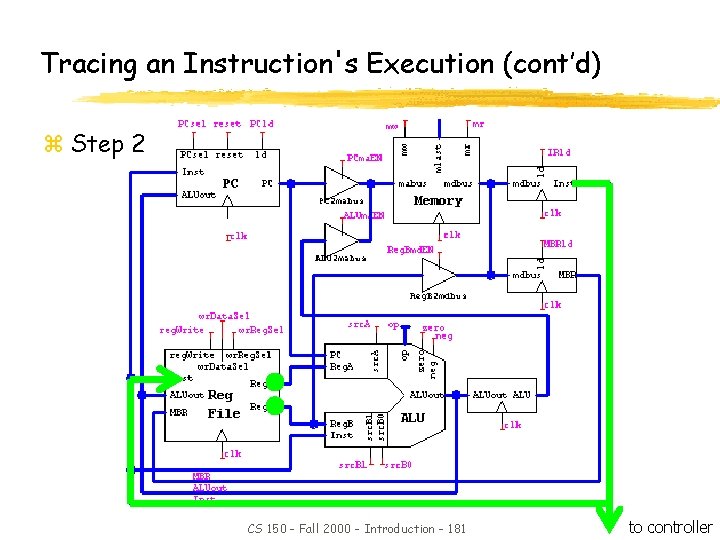
Tracing an Instruction's Execution z Instruction: R 0 r 3 = r 1 + r 2 rs=r 1 rt=r 2 rd=r 3 funct=0 z 1. Instruction fetch y Move instruction address from PC to memory address bus y Assert memory read y Move data from memory data bus into IR y Configure ALU to add 1 to PC y Configure PC to store new value from ALUout z 2. Instruction decode y Op-code bits of IR are input to control FSM y Rest of IR bits encode the operand addresses (rs and rt) x. These go to register file CS 150 - Fall 2000 - Introduction - 178

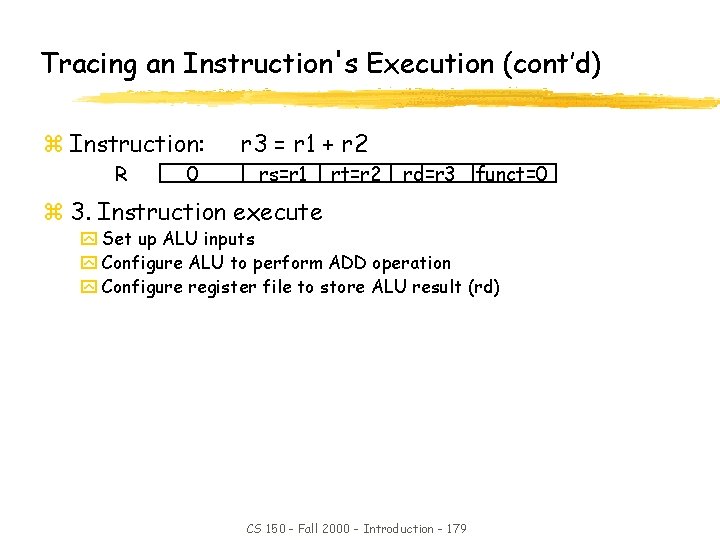
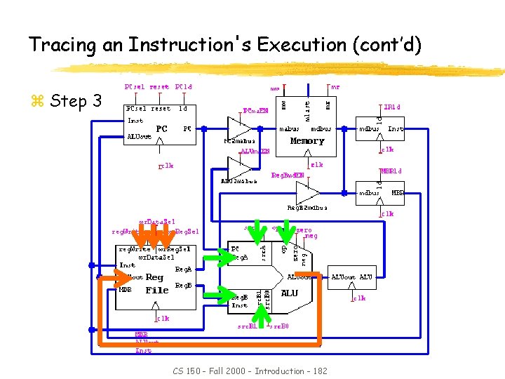
Tracing an Instruction's Execution (cont’d) z Instruction: R 0 r 3 = r 1 + r 2 rs=r 1 rt=r 2 rd=r 3 funct=0 z 3. Instruction execute y Set up ALU inputs y Configure ALU to perform ADD operation y Configure register file to store ALU result (rd) CS 150 - Fall 2000 - Introduction - 179

Tracing an Instruction's Execution (cont’d) z Step 1 CS 150 - Fall 2000 - Introduction - 180

Tracing an Instruction's Execution (cont’d) z Step 2 CS 150 - Fall 2000 - Introduction - 181 to controller

Tracing an Instruction's Execution (cont’d) z Step 3 CS 150 - Fall 2000 - Introduction - 182

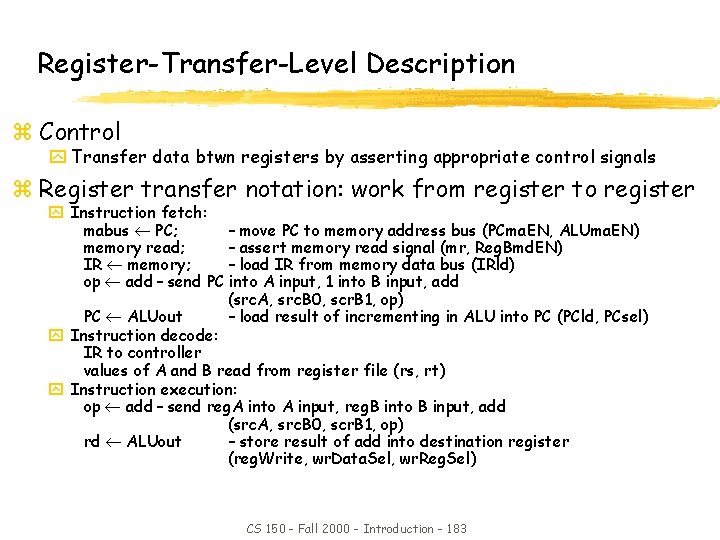
Register-Transfer-Level Description z Control y Transfer data btwn registers by asserting appropriate control signals z Register transfer notation: work from register to register y Instruction fetch: mabus PC; – move PC to memory address bus (PCma. EN, ALUma. EN) memory read; – assert memory read signal (mr, Reg. Bmd. EN) IR memory; – load IR from memory data bus (IRld) op add – send PC into A input, 1 into B input, add (src. A, src. B 0, scr. B 1, op) PC ALUout – load result of incrementing in ALU into PC (PCld, PCsel) y Instruction decode: IR to controller values of A and B read from register file (rs, rt) y Instruction execution: op add – send reg. A into A input, reg. B into B input, add (src. A, src. B 0, scr. B 1, op) rd ALUout – store result of add into destination register (reg. Write, wr. Data. Sel, wr. Reg. Sel) CS 150 - Fall 2000 - Introduction - 183

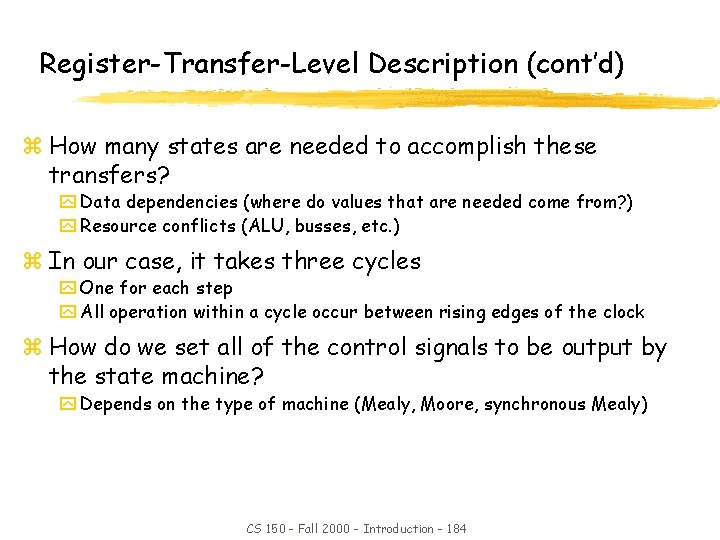
Register-Transfer-Level Description (cont’d) z How many states are needed to accomplish these transfers? y Data dependencies (where do values that are needed come from? ) y Resource conflicts (ALU, busses, etc. ) z In our case, it takes three cycles y One for each step y All operation within a cycle occur between rising edges of the clock z How do we set all of the control signals to be output by the state machine? y Depends on the type of machine (Mealy, Moore, synchronous Mealy) CS 150 - Fall 2000 - Introduction - 184
![Review of FSM Timing decode fetch step 1 step 2 IR memPC PC Review of FSM Timing decode fetch step 1 step 2 IR mem[PC]; PC +](https://slidetodoc.com/presentation_image_h/8cbe0f008d5c687ce56224042028dfe6/image-185.jpg)
Review of FSM Timing decode fetch step 1 step 2 IR mem[PC]; PC + 1; A rs B rt execute step 3 rd A + B to configure the data-path to do this here, when do we set the control signals? CS 150 - Fall 2000 - Introduction - 185

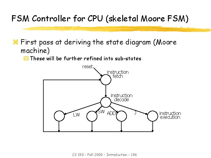
FSM Controller for CPU (skeletal Moore FSM) z First pass at deriving the state diagram (Moore machine) y These will be further refined into sub-states reset instruction fetch instruction decode LW SW ADD J CS 150 - Fall 2000 - Introduction - 186 instruction execution

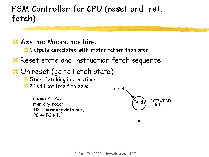
FSM Controller for CPU (reset and inst. fetch) z Assume Moore machine y Outputs associated with states rather than arcs z Reset state and instruction fetch sequence z On reset (go to Fetch state) y Start fetching instructions y PC will set itself to zero mabus PC; memory read; IR memory data bus; PC + 1; reset Fetch CS 150 - Fall 2000 - Introduction - 187 instruction fetch

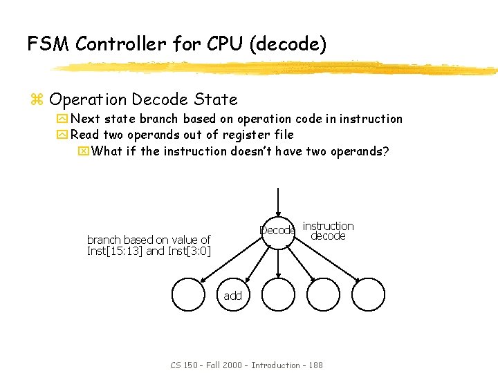
FSM Controller for CPU (decode) z Operation Decode State y Next state branch based on operation code in instruction y Read two operands out of register file x. What if the instruction doesn’t have two operands? Decode instruction decode branch based on value of Inst[15: 13] and Inst[3: 0] add CS 150 - Fall 2000 - Introduction - 188

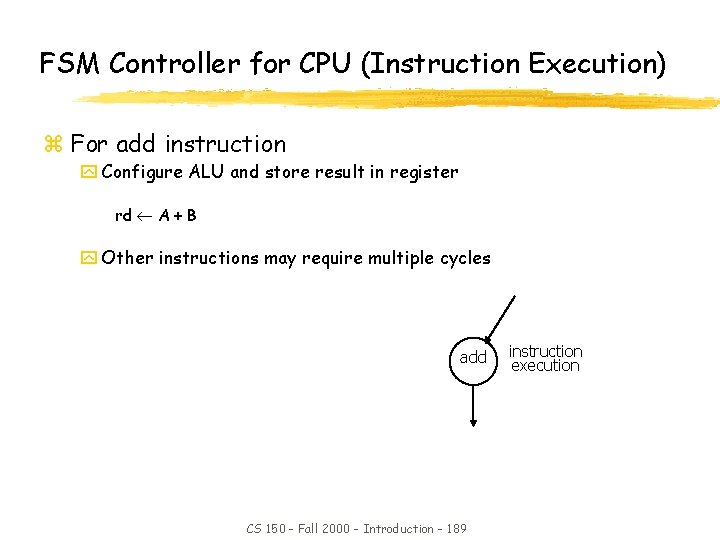
FSM Controller for CPU (Instruction Execution) z For add instruction y Configure ALU and store result in register rd A + B y Other instructions may require multiple cycles add CS 150 - Fall 2000 - Introduction - 189 instruction execution

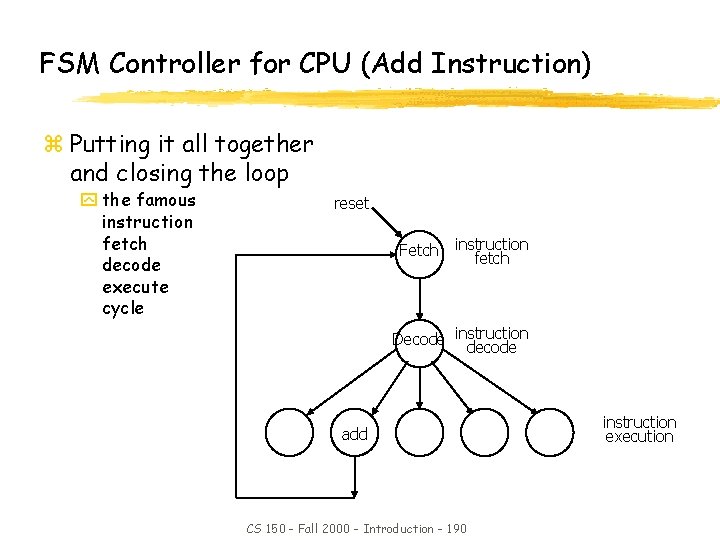
FSM Controller for CPU (Add Instruction) z Putting it all together and closing the loop y the famous instruction fetch decode execute cycle reset Fetch instruction fetch Decode instruction decode add CS 150 - Fall 2000 - Introduction - 190 instruction execution

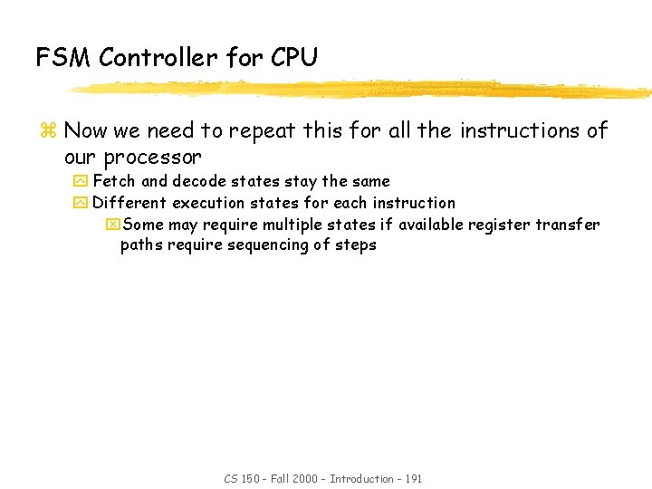
FSM Controller for CPU z Now we need to repeat this for all the instructions of our processor y Fetch and decode states stay the same y Different execution states for each instruction x. Some may require multiple states if available register transfer paths require sequencing of steps CS 150 - Fall 2000 - Introduction - 191