
EECS 150 Components and Design Techniques for Digital

- Slides: 40
EECS 150 - Components and Design Techniques for Digital Systems Lec 20 – RTL Design Optimization 11/6/2007 Shauki Elassaad Electrical Engineering and Computer Sciences University of California, Berkeley Slides adapted from Prof. Culler’s 2004 lecture http: //www-inst. eecs. berkeley. edu/~cs 150 1
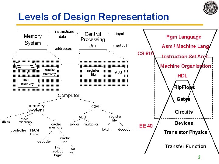
Levels of Design Representation Pgm Language Asm / Machine Lang CS 61 C Instruction Set Arch Machine Organization HDL Flip. Flops Gates Circuits EE 40 Devices Transistor Physics Transfer Function 2
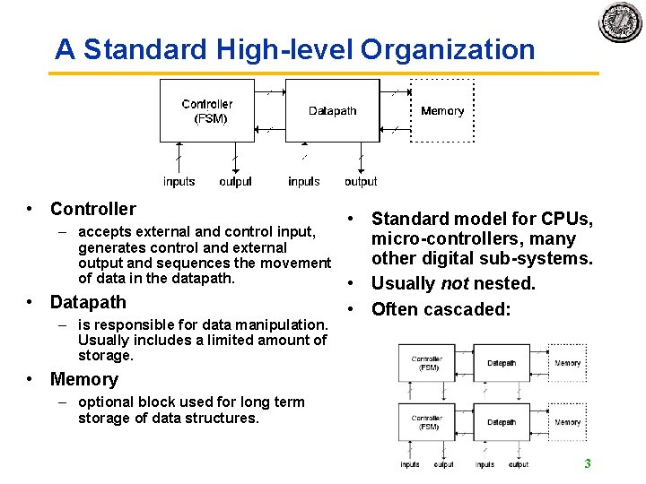
A Standard High-level Organization • Controller – accepts external and control input, generates control and external output and sequences the movement of data in the datapath. • Datapath – is responsible for data manipulation. Usually includes a limited amount of storage. • Standard model for CPUs, micro-controllers, many other digital sub-systems. • Usually not nested. • Often cascaded: • Memory – optional block used for long term storage of data structures. 3
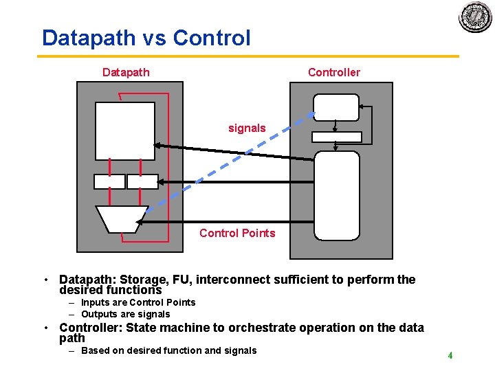
Datapath vs Control Datapath Controller signals Control Points • Datapath: Storage, FU, interconnect sufficient to perform the desired functions – Inputs are Control Points – Outputs are signals • Controller: State machine to orchestrate operation on the data path – Based on desired function and signals 4
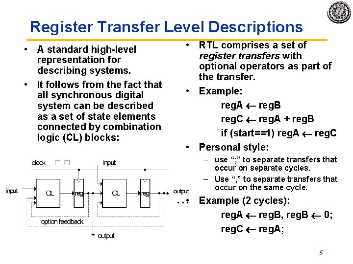
Register Transfer Level Descriptions • A standard high-level representation for describing systems. • It follows from the fact that all synchronous digital system can be described as a set of state elements connected by combination logic (CL) blocks: • RTL comprises a set of register transfers with optional operators as part of the transfer. • Example: reg. A reg. B reg. C reg. A + reg. B if (start==1) reg. A reg. C • Personal style: – use “; ” to separate transfers that occur on separate cycles. – Use “, ” to separate transfers that occur on the same cycle. • Example (2 cycles): reg. A reg. B, reg. B 0; reg. C reg. A; 5
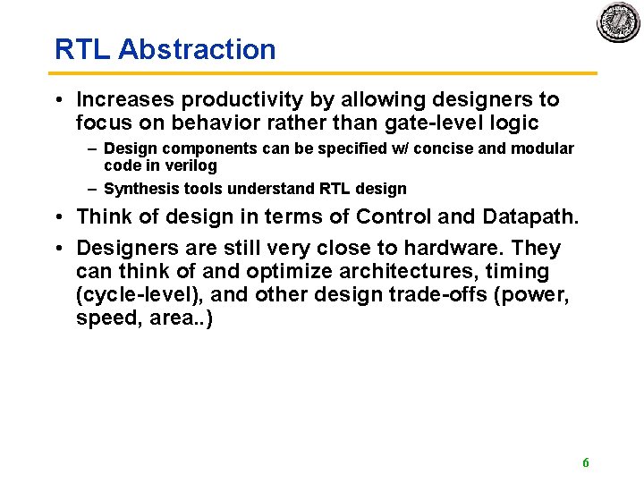
RTL Abstraction • Increases productivity by allowing designers to focus on behavior rather than gate-level logic – Design components can be specified w/ concise and modular code in verilog – Synthesis tools understand RTL design • Think of design in terms of Control and Datapath. • Designers are still very close to hardware. They can think of and optimize architectures, timing (cycle-level), and other design trade-offs (power, speed, area. . ) 6
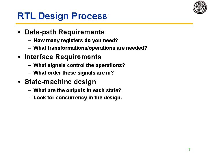
RTL Design Process • Data-path Requirements – How many registers do you need? – What transformations/operations are needed? • Interface Requirements – What signals control the operations? – What order these signals are in? • State-machine design – What are the outputs in each state? – Look for concurrency in the design. 7
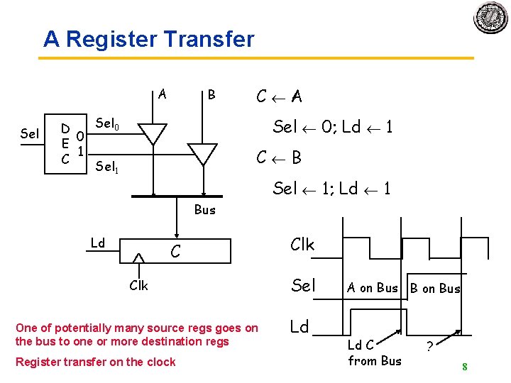
A Register Transfer A Sel B Sel 0 D 0 E 1 C Sel 1 C A Sel 0; Ld 1 C B Sel 1; Ld 1 Bus Ld C Clk One of potentially many source regs goes on the bus to one or more destination regs Register transfer on the clock Clk Sel Ld A on Bus B on Bus Ld C from Bus ? 8
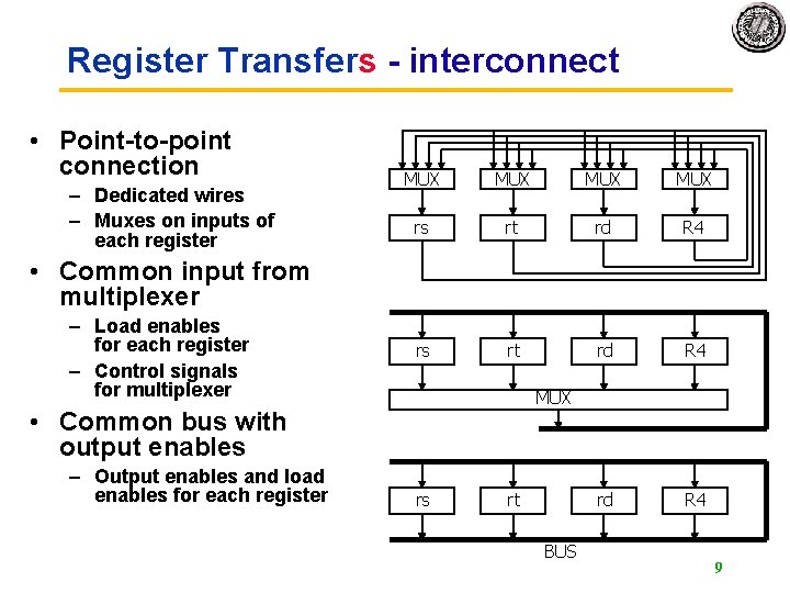
Register Transfers - interconnect • Point-to-point connection – Dedicated wires – Muxes on inputs of each register MUX MUX rs rt rd R 4 • Common input from multiplexer – Load enables for each register – Control signals for multiplexer MUX • Common bus with output enables – Output enables and load enables for each register rs rt BUS 9
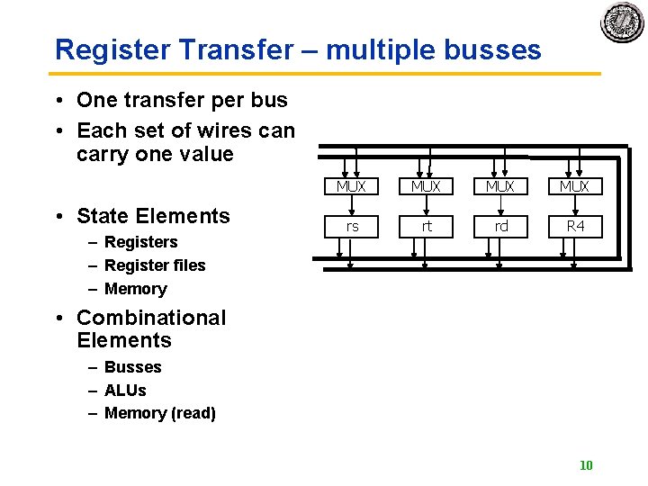
Register Transfer – multiple busses • One transfer per bus • Each set of wires can carry one value • State Elements – Register files – Memory MUX MUX rs rt rd R 4 • Combinational Elements – Busses – ALUs – Memory (read) 10
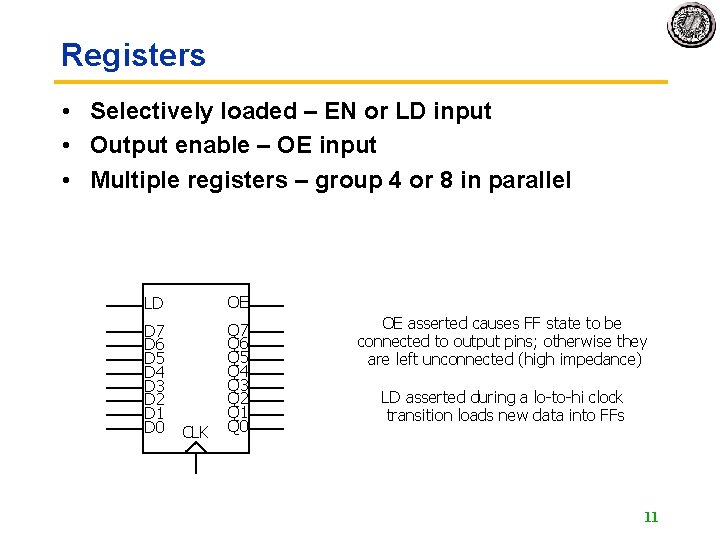
Registers • Selectively loaded – EN or LD input • Output enable – OE input • Multiple registers – group 4 or 8 in parallel LD OE D 7 D 6 D 5 D 4 D 3 D 2 D 1 D 0 Q 7 Q 6 Q 5 Q 4 Q 3 Q 2 Q 1 Q 0 CLK OE asserted causes FF state to be connected to output pins; otherwise they are left unconnected (high impedance) LD asserted during a lo-to-hi clock transition loads new data into FFs 11
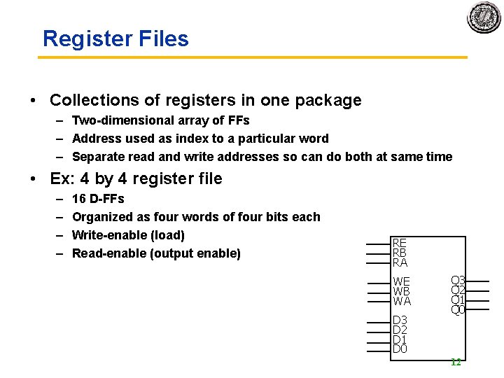
Register Files • Collections of registers in one package – Two-dimensional array of FFs – Address used as index to a particular word – Separate read and write addresses so can do both at same time • Ex: 4 by 4 register file – – 16 D-FFs Organized as four words of four bits each Write-enable (load) Read-enable (output enable) RE RB RA WE WB WA D 3 D 2 D 1 D 0 Q 3 Q 2 Q 1 Q 0 12
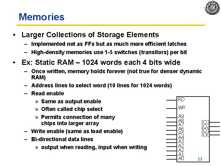
Memories • Larger Collections of Storage Elements – Implemented not as FFs but as much more efficient latches – High-density memories use 1 -5 switches (transitors) per bit • Ex: Static RAM – 1024 words each 4 bits wide – Once written, memory holds forever (not true for denser dynamic RAM) – Address lines to select word (10 lines for 1024 words) – Read enable RD » Same as output enable WR » Often called chip select A 9 » Permits connection of many A 8 IO 3 chips into larger array A 7 IO 2 A 6 IO 1 – Write enable (same as load enable) A 5 IO 0 A 4 – Bi-directional data lines A 3 A 2 » output when reading, input when writing A 2 A 1 A 0 13
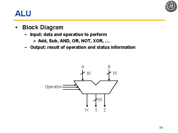
ALU • Block Diagram – Input: data and operation to perform » Add, Sub, AND, OR, NOT, XOR, … – Output: result of operation and status information A B 16 16 Operation 16 N S Z 14
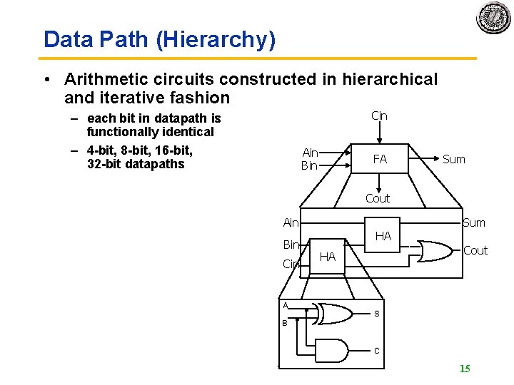
Data Path (Hierarchy) • Arithmetic circuits constructed in hierarchical and iterative fashion Cin – each bit in datapath is functionally identical – 4 -bit, 8 -bit, 16 -bit, 32 -bit datapaths Ain Bin FA Sum Cout Ain Bin Cin HA HA Sum Cout 15
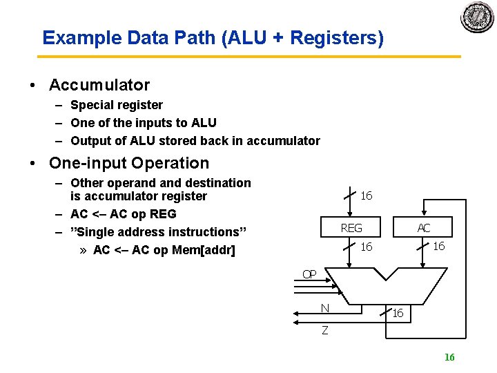
Example Data Path (ALU + Registers) • Accumulator – Special register – One of the inputs to ALU – Output of ALU stored back in accumulator • One-input Operation – Other operand destination is accumulator register – AC <– AC op REG – ”Single address instructions” » AC <– AC op Mem[addr] 16 REG AC 16 16 OP N 16 Z 16
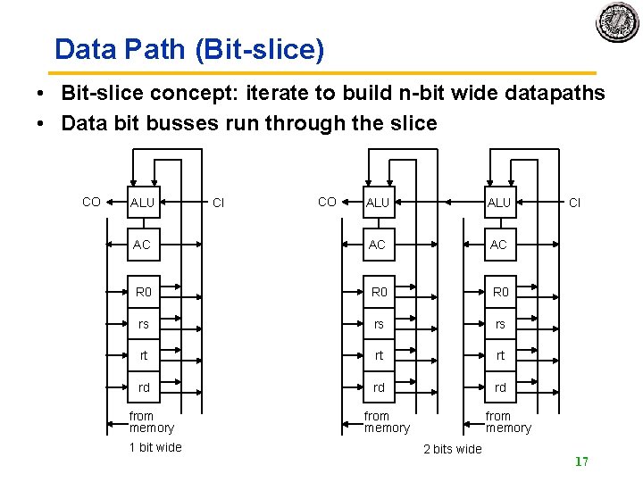
Data Path (Bit-slice) • Bit-slice concept: iterate to build n-bit wide datapaths • Data bit busses run through the slice CO ALU ALU AC AC AC R 0 R 0 rs rs rs rt rt rt rd rd rd from memory 1 bit wide CI from memory 2 bits wide 17
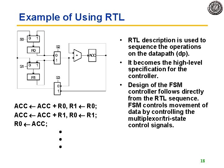
Example of Using RTL ACC + R 0, R 1 R 0; ACC + R 1, R 0 R 1; R 0 ACC; • RTL description is used to sequence the operations on the datapath (dp). • It becomes the high-level specification for the controller. • Design of the FSM controller follows directly from the RTL sequence. FSM controls movement of data by controlling the multiplexor/tri-state control signals. 18
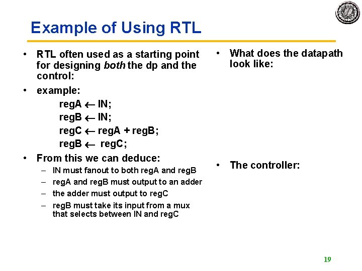
Example of Using RTL • RTL often used as a starting point for designing both the dp and the control: • example: reg. A IN; reg. B IN; reg. C reg. A + reg. B; reg. B reg. C; • From this we can deduce: – – IN must fanout to both reg. A and reg. B must output to an adder the adder must output to reg. C reg. B must take its input from a mux that selects between IN and reg. C • What does the datapath look like: • The controller: 19
Announcements • Lab Etiquette – Food in the lab is still a problem. If problem persists, we will be forced to close th • Discussion sessions are on for this week. • No Lab Lecture this week 20
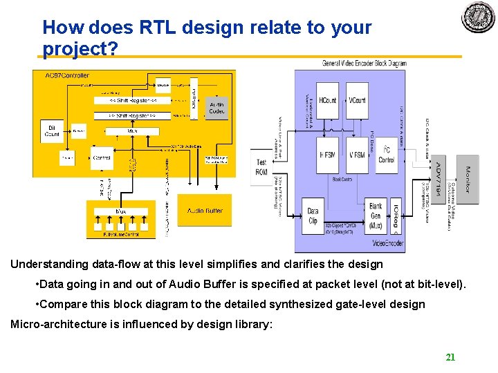
How does RTL design relate to your project? Understanding data-flow at this level simplifies and clarifies the design • Data going in and out of Audio Buffer is specified at packet level (not at bit-level). • Compare this block diagram to the detailed synthesized gate-level design Micro-architecture is influenced by design library: 21
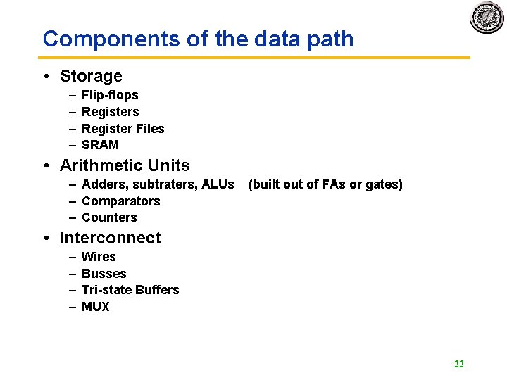
Components of the data path • Storage – – Flip-flops Register Files SRAM • Arithmetic Units – Adders, subtraters, ALUs (built out of FAs or gates) – Comparators – Counters • Interconnect – – Wires Busses Tri-state Buffers MUX 22
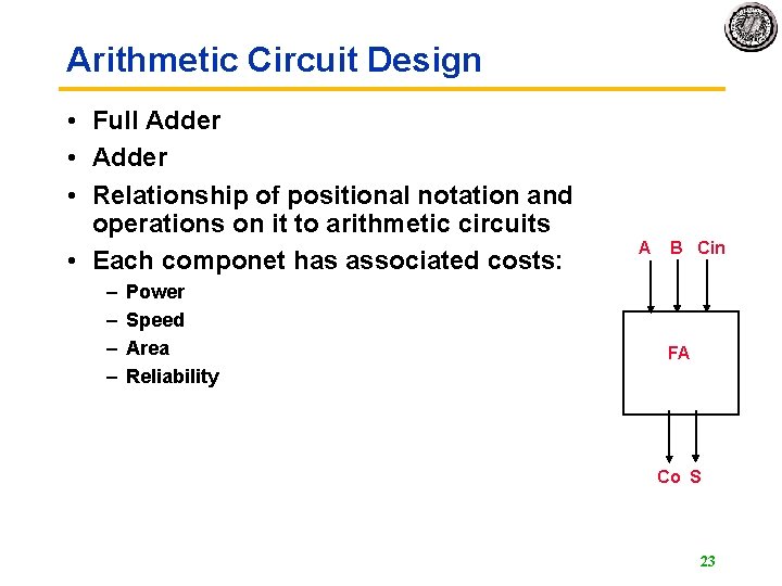
Arithmetic Circuit Design • Full Adder • Relationship of positional notation and operations on it to arithmetic circuits • Each componet has associated costs: – – Power Speed Area Reliability A B Cin FA Co S 23
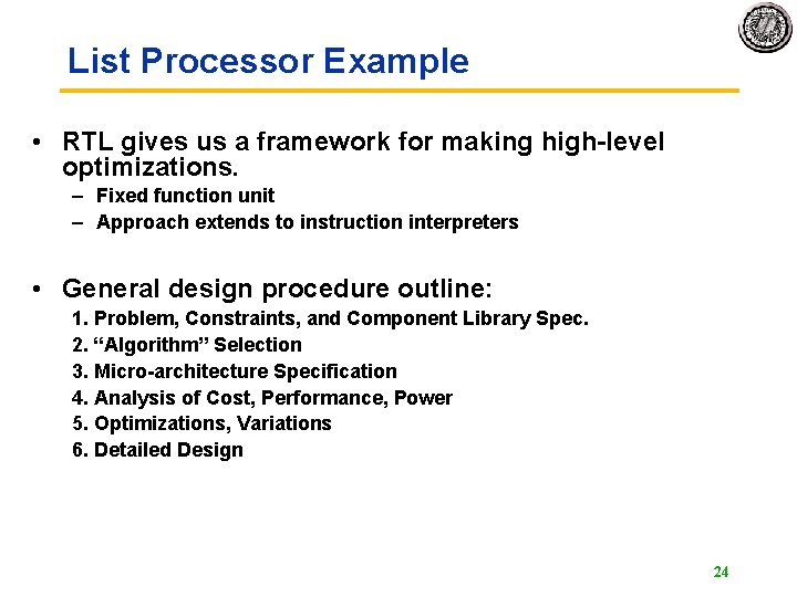
List Processor Example • RTL gives us a framework for making high-level optimizations. – Fixed function unit – Approach extends to instruction interpreters • General design procedure outline: 1. Problem, Constraints, and Component Library Spec. 2. “Algorithm” Selection 3. Micro-architecture Specification 4. Analysis of Cost, Performance, Power 5. Optimizations, Variations 6. Detailed Design 24
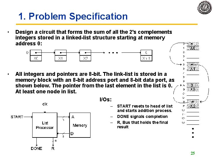
1. Problem Specification • Design a circuit that forms the sum of all the 2's complements integers stored in a linked-list structure starting at memory address 0: • All integers and pointers are 8 -bit. The link-list is stored in a memory block with an 8 -bit address port and 8 -bit data port, as shown below. The pointer from the last element in the list is 0. At least one node in list. I/Os: – START resets to head of list and starts addition process. – DONE signals completion – R, Bus that holds the final result 25
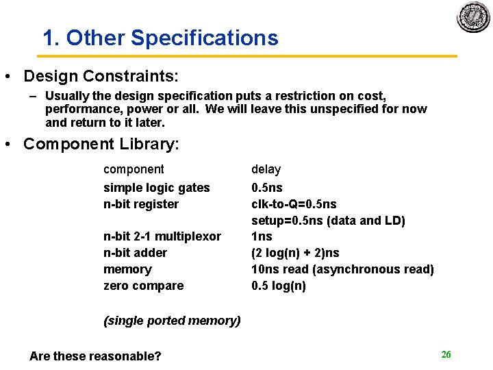
1. Other Specifications • Design Constraints: – Usually the design specification puts a restriction on cost, performance, power or all. We will leave this unspecified for now and return to it later. • Component Library: component delay simple logic gates n-bit register 0. 5 ns clk-to-Q=0. 5 ns setup=0. 5 ns (data and LD) 1 ns (2 log(n) + 2)ns 10 ns read (asynchronous read) 0. 5 log(n) n-bit 2 -1 multiplexor n-bit adder memory zero compare (single ported memory) Are these reasonable? 26
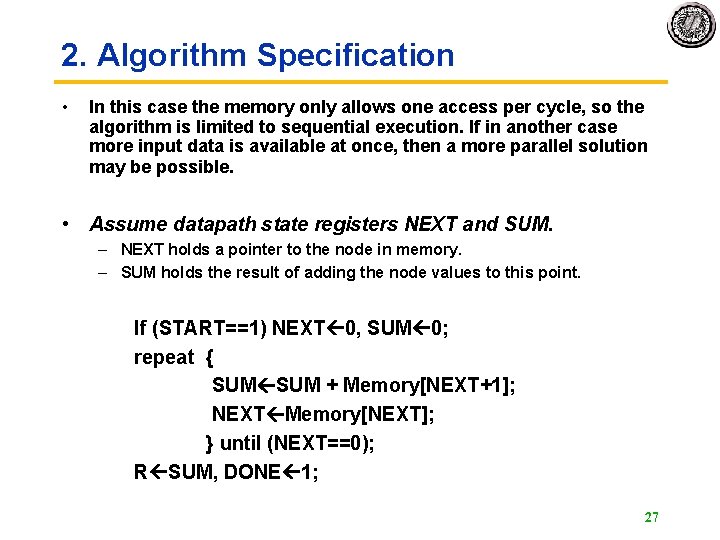
2. Algorithm Specification • In this case the memory only allows one access per cycle, so the algorithm is limited to sequential execution. If in another case more input data is available at once, then a more parallel solution may be possible. • Assume datapath state registers NEXT and SUM. – NEXT holds a pointer to the node in memory. – SUM holds the result of adding the node values to this point. If (START==1) NEXT 0, SUM 0; repeat { SUM + Memory[NEXT+1]; NEXT Memory[NEXT]; } until (NEXT==0); R SUM, DONE 1; 27
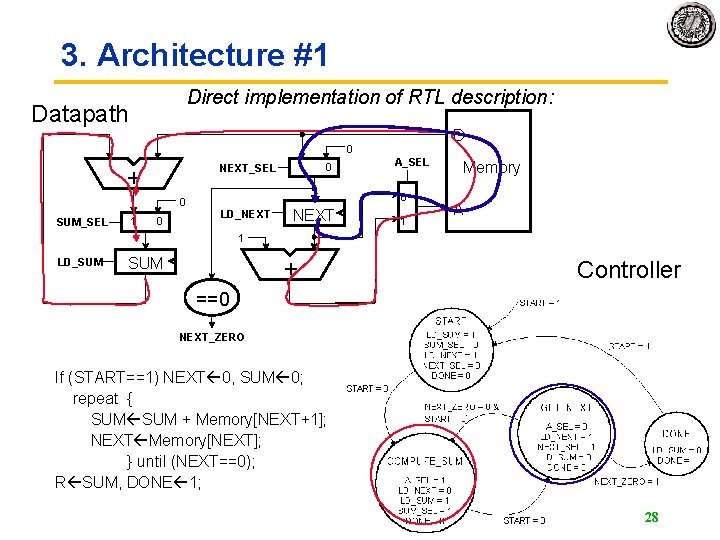
3. Architecture #1 Direct implementation of RTL description: Datapath D 0 + 0 SUM_SEL 1 1 NEXT_SEL 0 0 A_SEL 0 LD_NEXT 1 Memory A 1 LD_SUM + Controller ==0 NEXT_ZERO If (START==1) NEXT 0, SUM 0; repeat { SUM + Memory[NEXT+1]; NEXT Memory[NEXT]; } until (NEXT==0); R SUM, DONE 1; 28
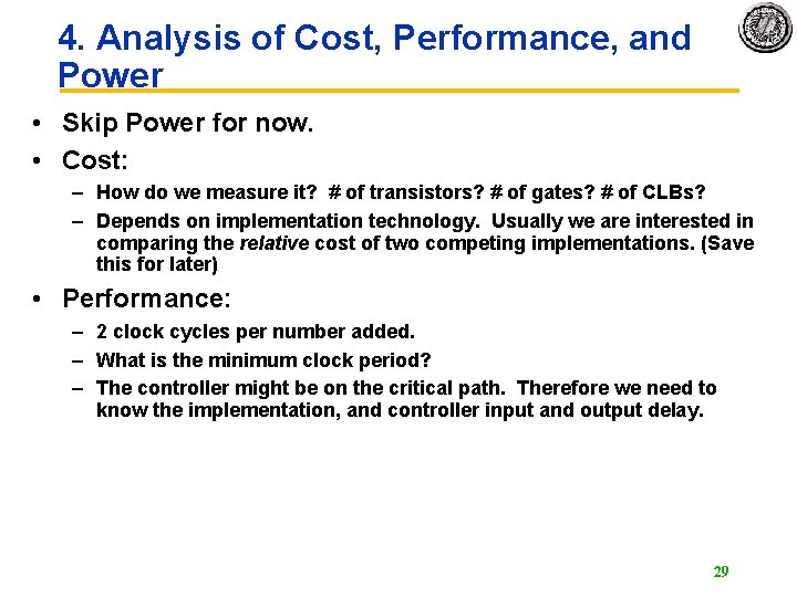
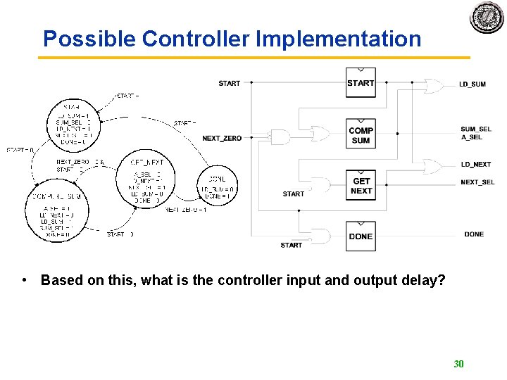
4. Analysis of Cost, Performance, and Power • Skip Power for now. • Cost: – How do we measure it? # of transistors? # of gates? # of CLBs? – Depends on implementation technology. Usually we are interested in comparing the relative cost of two competing implementations. (Save this for later) • Performance: – 2 clock cycles per number added. – What is the minimum clock period? – The controller might be on the critical path. Therefore we need to know the implementation, and controller input and output delay. 29
Possible Controller Implementation • Based on this, what is the controller input and output delay? 30
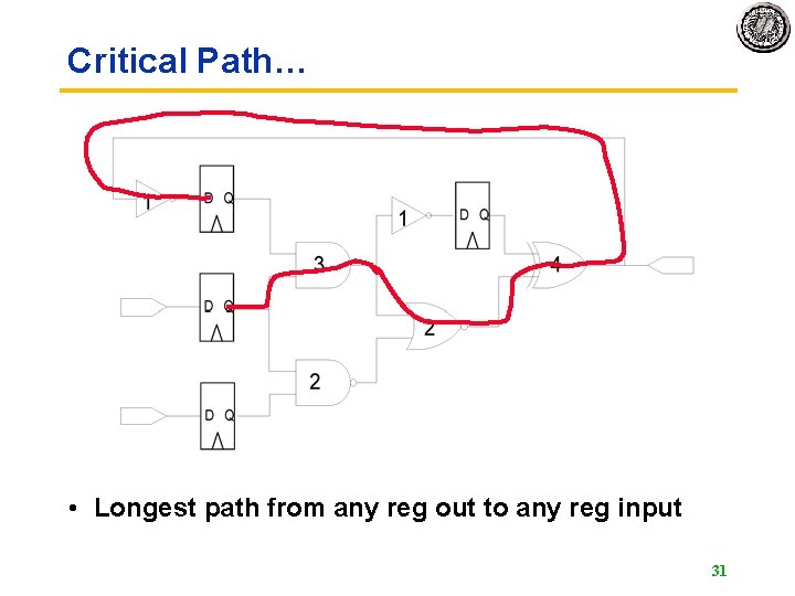
Critical Path… • Longest path from any reg out to any reg input 31
4. Analysis of Performance 32
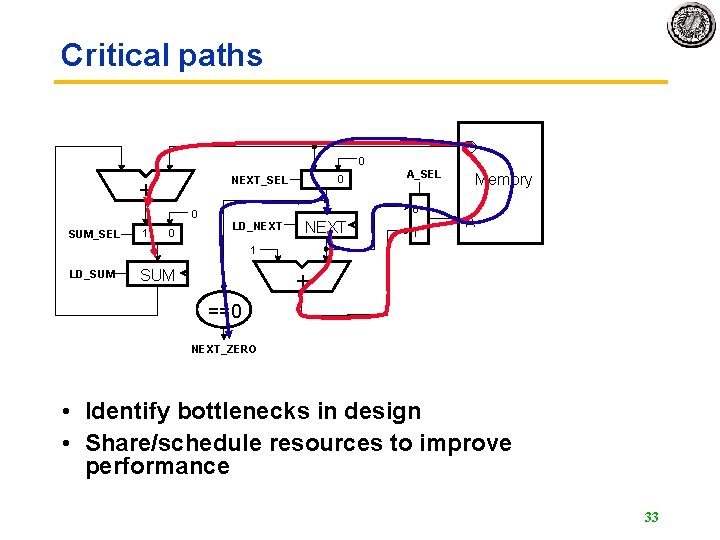
Critical paths D 0 + 0 SUM_SEL 1 1 NEXT_SEL 0 0 A_SEL 0 LD_NEXT 1 Memory A 1 LD_SUM + ==0 NEXT_ZERO • Identify bottlenecks in design • Share/schedule resources to improve performance 33
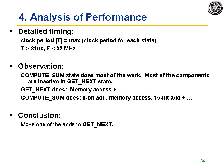
4. Analysis of Performance • Detailed timing: clock period (T) = max (clock period for each state) T > 31 ns, F < 32 MHz • Observation: COMPUTE_SUM state does most of the work. Most of the components are inactive in GET_NEXT state. GET_NEXT does: Memory access + … COMPUTE_SUM does: 8 -bit add, memory access, 15 -bit add + … • Conclusion: Move one of the adds to GET_NEXT. 34
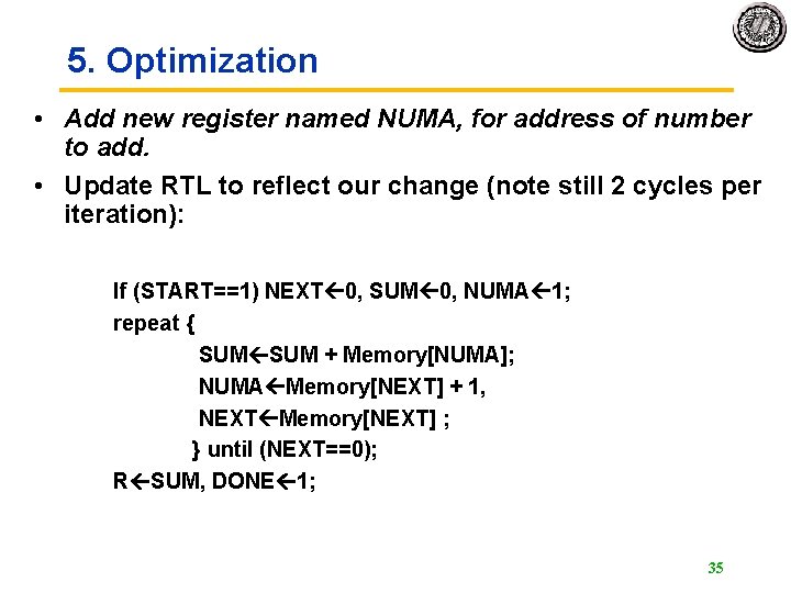
5. Optimization • Add new register named NUMA, for address of number to add. • Update RTL to reflect our change (note still 2 cycles per iteration): If (START==1) NEXT 0, SUM 0, NUMA 1; repeat { SUM + Memory[NUMA]; NUMA Memory[NEXT] + 1, NEXT Memory[NEXT] ; } until (NEXT==0); R SUM, DONE 1; 35
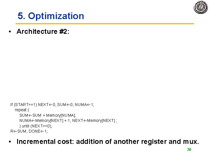
5. Optimization • Architecture #2: If (START==1) NEXT 0, SUM 0, NUMA 1; repeat { SUM + Memory[NUMA]; NUMA Memory[NEXT] + 1, NEXT Memory[NEXT] ; } until (NEXT==0); R SUM, DONE 1; • Incremental cost: addition of another register and mux. 36
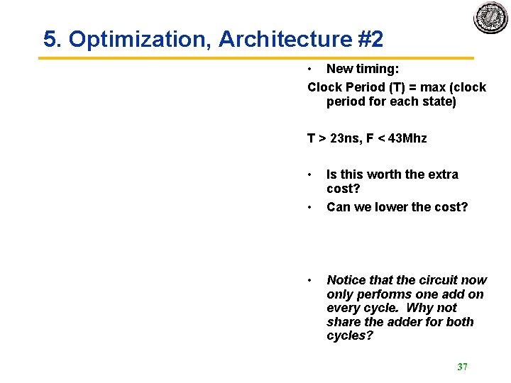
5. Optimization, Architecture #2 • New timing: Clock Period (T) = max (clock period for each state) T > 23 ns, F < 43 Mhz • • • Is this worth the extra cost? Can we lower the cost? Notice that the circuit now only performs one add on every cycle. Why not share the adder for both cycles? 37
5. Optimization, Architecture #3 • Incremental cost: – Addition of another mux and control. Removal of an 8 -bit adder. • Performance: – mux adds 1 ns to cycle time. 24 ns, 41. 67 MHz. • Is the cost savings worth the performance degradation? 38
Design Complexity & Productivity Gap • Design gap is accelerating with advances in processing technology. • RTL Designers must identify downstream problems — timing, signal integrity, reliability, and others — prior to synthesis and be able to implement design fixes where they will have a more significant impact on chip performance. • The key to a successful design is design closure. The various performance specifications comprising timing, power, and reliability, along with chip cost, are all closely coupled. EETimes 08/22/2003 39
Design Gap • Keeping up with Moore's Law requires the implementation of disruptive design technology every few years. • A common theme of advancing design technology is the continuing move to higher design abstraction levels. 40