Midterm Exam Question Thermal doping review This presentation


- Slides: 7

Midterm Exam Question (Thermal doping review) This presentation is partially animated. Only use the control panel at the bottom of screen to review what you have seen. When using your mouse, make sure you click only when it is within the light blue frame that surrounds each slide.

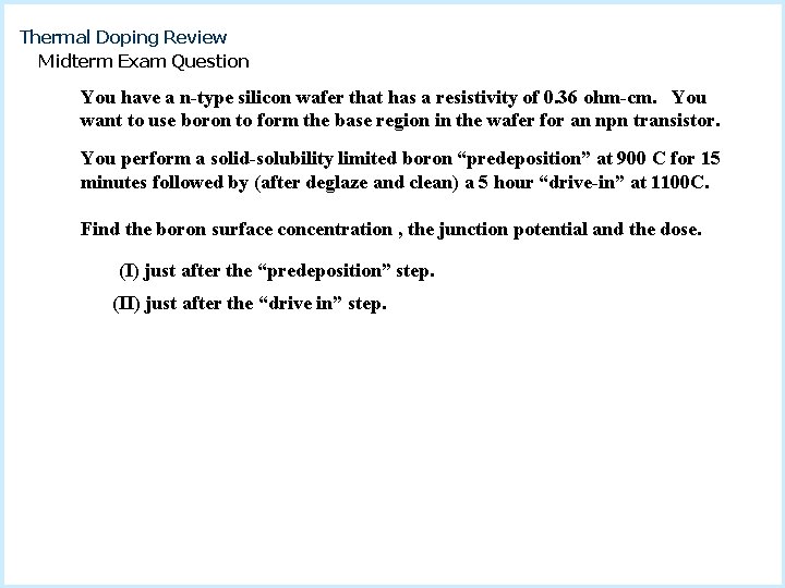
Thermal Doping Review Midterm Exam Question You have a n-type silicon wafer that has a resistivity of 0. 36 ohm-cm. You want to use boron to form the base region in the wafer for an npn transistor. You perform a solid-solubility limited boron “predeposition” at 900 C for 15 minutes followed by (after deglaze and clean) a 5 hour “drive-in” at 1100 C. Find the boron surface concentration , the junction potential and the dose. (I) just after the “predeposition” step. (II) just after the “drive in” step.

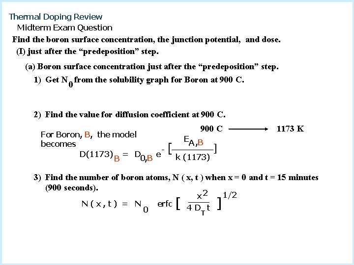
Thermal Doping Review Midterm Exam Question Find the boron surface concentration, the junction potential, and dose. (I) just after the “predeposition” step. (a) Boron surface concentration just after the “predeposition” step. 1) Get N from the solubility graph for Boron at 900 C. 0 2) Find the value for diffusion coefficient at 900 C. For Boron, B, the model becomes D(1173) = D 0, B e B 900 C [ E , B A k (1173) 1173 K ] 3) Find the number of boron atoms, N ( x, t ) when x = 0 and t = 15 minutes (900 seconds). N(x, t) = N 0 erfc [ x 2 4 D t T ] 1/2

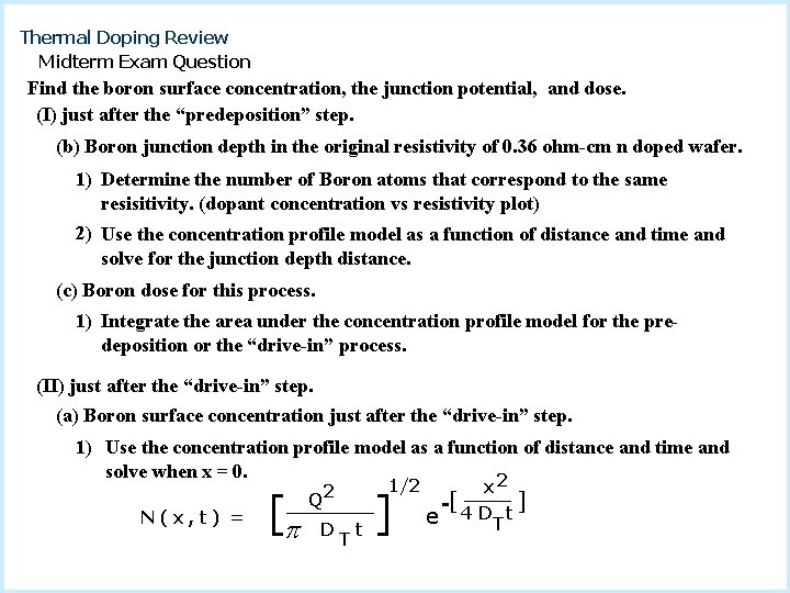
Thermal Doping Review Midterm Exam Question Find the boron surface concentration, the junction potential, and dose. (I) just after the “predeposition” step. (b) Boron junction depth in the original resistivity of 0. 36 ohm-cm n doped wafer. 1) Determine the number of Boron atoms that correspond to the same resisitivity. (dopant concentration vs resistivity plot) 2) Use the concentration profile model as a function of distance and time and solve for the junction depth distance. (c) Boron dose for this process. 1) Integrate the area under the concentration profile model for the predeposition or the “drive-in” process. (II) just after the “drive-in” step. (a) Boron surface concentration just after the “drive-in” step. 1) Use the concentration profile model as a function of distance and time and solve when x = 0. 2 N(x, t) = [p Q 1/2 2 D T t ] e -[ 4 x ] D t T

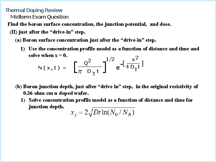
Thermal Doping Review Midterm Exam Question Find the boron surface concentration, the junction potential, and dose. (II) just after the “drive-in” step. (a) Boron surface concentration just after the “drive-in” step. 1) Use the concentration profile model as a function of distance and time and solve when x = 0. 2 N(x, t) = [p Q 1/2 2 D T t ] e -[ 4 x ] D t T (b) Boron junction depth, just after “drive in” step, in the original resistivity of 0. 36 ohm-cm n doped wafer. 1) Solve concentration profile model as a function of distance and time for junction depth.

Thermal Doping Review Midterm Exam Question Find the boron surface concentration, the junction potential, and dose. (II) just after the “drive-in” step. (a) Boron surface concentration just after the “drive-in” step. 1) Use the concentration profile model as a function of distance and time and solve when x = 0. 2 N(x, t) = [p Q 1/2 2 D T t ] e -[ 4 x ] D t T (b) Boron junction depth, just after “drive in” step, in the original resistivity of 0. 36 ohm-cm n doped wafer. 1) Solve concentration profile model as a function of distance and time for junction depth.

Find the boron surface concentration, the junction potential, and dose. (II) just after the “drive-in” step. (a) Boron surface concentration just after the “drive-in” step. 1) Use the concentration profile model as a function of distance and time and solve when x = 0. 2 N(x, t) = [p Q 1/2 2 D T t ] e -[ 4 x ] D t T (b) Boron junction depth, just after “drive in” step, in the original resistivity of 0. 36 ohm-cm n doped wafer. 1) Solve concentration profile model as a function of distance and time for junction depth.