Serial Communication Data Communications Data communications refers to


 for serial data")


 Block diagram and (b)")


 and base word")

")

")

")

")

")

")

")

 flip-flop within")


 The F/L")
 output")


 are decoded")

 Ø Return mode=100 (Return")


.")


 • General algorithm for ADC")
 • • • Analog input")
 ADC 0808/0809 : • The")
 • ADD A, ADD B,")
")
 • If one needs a")
 • • I/P 0 –I/P")
")
")
 • Example: Interfacing ADC 0808")
 • Port A acts as")
 • • • MOV AL,")
")


 for serial data")


 • This is bidirectional data")
 • This is a clock input signal which determines")
 • CLK signal is used to generate internal device")
 • This is an output terminal which indicates that")
 • This is an output terminal which indicates that")
 • This is an input terminal which receives a")
 • This is an output terminal for transmitting data")
 This is a terminal which receives serial data.")
 • This is a clock input signal which determines")

 • This is an output port for MODEM interface.")

 Mode Instruction • Mode instruction is used for setting the function of the")


- Slides: 156
Serial Communication
Data Communications • Data communications refers to the ability of one computer to exchange data with another computer or a peripheral • Physically, the data comm. path may be a short, 5 to 10 feet ribbon cable connecting a microcomputer and parallel printer; or it might be a high speed telecommunications port connecting two computers thousands of miles apart. • Standard data communication interfaces and standards are needed • Centronic’s parallel printerface • RS-232 defines a serial communications standard • We focus on serial I/O this week • 8251 USART (Universal Synchronous/Asynchronous Receiver/Transmitter) is the key component for converting parallel data to serial form and vice versa • Two types of serial data communications are widely used – Asynchronous communications – Synchronous communications
Types of Transmission
8251 A programmable Communication Interface
Introduction 8251 A is a USART (Universal Synchronous Asynchronous Receiver Transmitter) for serial data communication. Programmable peripheral designed for synchronous /asynchronous serial data communication, packaged in a 28 -pin DIP. Receives parallel data from the CPU & transmits serial data after conversion. Also receives serial data from the outside & transmits parallel data to the CPU after conversion.
Pin diagram
Block diagram of the 8251 USART
Sections of 8251 A Data Bus buffer Read/Write Control Logic Modem Control Transmitter Receiver 1. Data Bus Buffer D 0 -D 7 : 8 -bit data bus used to read or write status, command word or data from or to the 8251 A
2. Read/Write Control logic • Includes a control logic, six input signals & three buffer registers: Data register, control register & status register. • Control logic : Interfaces the chip with MPU, determines the functions of the chip according to the control word in the control register & monitors the data flow.
Input signals CS – Chip Select : When signal goes low, the 8251 A is selected by the MPU for communication. C/D – Control/Data : When signal is high, the control or status register is addressed; when it is low, data buffer is addressed. (Control register & status register are differentiated by WR and RD signals) WR : When signal is low, the MPU either writes in the control register or sends output to the data buffer. RD : When signal goes low, the MPU either reads a status from the status register or accepts data from data buffer. RESET : A high on this signal reset 8252 A & forces it into the idle mode. CLK : Clock input, usually connected to the system clock for communication with the microprocessor.
Control Register 16 -bit register for a control word consist of two independent bytes namely mode word & command word. Mode word : Specifies the general characteristics of operation such as baud, parity, number of bits etc. Command word : Enables the data transmission and reception. Register can be accessed as an output port when the Control/Data pin is high.
Status register • Checks the ready status of the peripheral. • Status word in the status register provides the information concerning register status and transmission errors. Data register Used as an input and output port when the C/D is low CS C/D WR RD Operation 0 0 1 1 0 0 1 × 0 0 1 1 × 0 1 1 0 × MPU reads data from data buffer MPU writes a word to control register MPU reads a word from status register Chip is not selected for any operation
3. Modem Control DSR - Data Set Ready : Checks if the Data Set is ready when communicating with a modem. DTR - Data Terminal Ready : Indicates that the device is ready to accept data when the 8251 is communicating with a modem. CTS - Clear to Send : If its low, the 8251 A is enabled to transmit the serial data provided the enable bit in the command byte is set to ‘ 1’. RTS - Request to Send Data : Low signal indicates the modem that the receiver is ready to receive a data byte from the modem.
4. Transmitter section Accepts parallel data from MPU & converts them into serial data. Has two registers: Buffer register : To hold eight bits Output register : To convert eight bits into a stream of serial bits.
The MPU writes a byte in the buffer register. Whenever the output register is empty; the contents of buffer register are transferred to output register. Transmitter section consists of three output & one input signals Tx. D - Transmitted Data Output : Output signal to transmit the data to peripherals Tx. C - Transmitter Clock Input : Input signal, controls the rate of transmission. Tx. RDY - Transmitter Ready : Output signal, indicates the buffer register is empty and the USART is ready to accept the next data byte. Tx. E - Transmitter Empty : Output signal to indicate the output register is empty and the USART is ready to accept the next data byte.
5. Receiver Section Accepts serial data on the Rx. D pin and converts them to parallel data. Has two registers : Receiver input register Buffer register Input Register Rx. D Receive Buffer Rx. RDY Receive control Rx. C
When Rx. D goes low, the control logic assumes it is a start bit, waits for half bit time, and samples the line again. If the line is still low, the input register accepts the following data, and loads it into buffer register at the rate determined by the receiver clock. Rx. RDY - Receiver Ready Output: Output signal, goes high when the USART has a character in the buffer register & is ready to transfer it to the MPU. Rx. D - Receive Data Input : Bits are received serially on this line & converted into a parallel byte in the receiver input register. Rx. C - Receiver Clock Input : Clock signal that controls the rate at which bits are received by the USART.
DMA Controller 8237
Introduction • The DMA I/O technique provides direct access to the memory while the microprocessor is temporarily disabled. • This chapter also explains the operation of disk memory systems and video systems that are often DMA-processed. • Disk memory includes floppy, fixed, and optical disk storage. Video systems include digital and analog monitors.
13– 1 BASIC DMA OPERATION • Two control signals are used to request and acknowledge a direct memory access (DMA) transfer in the microprocessor-based system. – the HOLD pin is an input used to request a DMA action – the HLDA pin is an output that acknowledges the DMA action • Figure 13– 1 shows the timing that is typically found on these two DMA control pins.
Figure 13– 1 HOLD and HLDA timing for the microprocessor. – HOLD is sampled in any clocking cycle – when the processor recognizes the hold, it stops executing software and enters hold cycles – HOLD input has higher priority than INTR or NMI – the only microprocessor pin that has a higher priority than a HOLD is the RESET pin
• HLDA becomes active to indicate the processor has placed its buses at high -impedance state. – as can be seen in the timing diagram, there a few clock cycles between the time that HOLD changes and until HLDA changes • HLDA output is a signal to the requesting device that the processor has relinquished control of its memory and I/O space. – one could call HOLD input a DMA request input and HLDA output a DMA grant signal
Basic DMA Definitions • Direct memory accesses normally occur between an I/O device and memory without the use of the microprocessor. – a DMA read transfers data from the memory to the I/O device – A DMA write transfers data from an I/O device to memory • Memory & I/O are controlled simultaneously. – which is why the system contains separate memory and I/O control signals
• A DMA read causes the MRDC and IOWC signals to activate simultaneously. – transferring data from memory to the I/O device • A DMA write causes the MWTC and IORC signals to both activate. • 8086/8088 require a controller or circuit such as shown in Fig 13– 2 for control bus signal generation. • The DMA controller provides memory with its address, and controller signal (DACK) selects the I/O device during the transfer.
Figure 13– 2 A circuit that generates system control signals in a DMA environment.
• Data transfer speed is determined by speed of the memory device or a DMA controller. – if memory speed is 50 ns, DMA transfers occur at rates up to 1/50 ns or 20 M bytes per second – if the DMA controller functions at a maximum rate of 15 MHz with 50 ns memory, maximum transfer rate is 15 MHz because the DMA controller is slower than the memory • In many cases, the DMA controller slows the speed of the system when transfers occur.
• The switch to serial data transfers in modern systems has made DMA is less important. • The serial PCI Express bus transfers data at rates exceeding DMA transfers. • The SATA (serial ATA) interface for disk drives uses serial transfers at the rate of 300 Mbps – and has replaced DMA transfers for hard disks • Serial transfers on main-boards between components using can approach 20 Gbps for the PCI Express connection .
13– 2 THE 8237 DMA CONTROLLER • The 8237 supplies memory & I/O with control signals and memory address information during the DMA transfer. – actually a special-purpose microprocessor whose job is high-speed data transfer between memory and I/O • Figure 13– 3 shows the pin-out and block diagram of the 8237 programmable DMA controller.
Figure 13– 3 The 8237 A-5 programmable DMA controller. (a) Block diagram and (b) pin-out. (Courtesy of Intel Corporation. )
• 8237 is not a discrete component in modern microprocessor-based systems. – it appears within many system controller chip sets • 8237 is a four-channel device compatible with 8086/8088, adequate for small systems. – expandable to any number of DMA channel inputs • 8237 is capable of DMA transfers at rates up to 1. 6 M bytes per second. – each channel is capable of addressing a full 64 K-byte section of memory and transfer up to 64 K bytes with a single programming
CLK 8237 Pin Definitions • Clock input is connected to the system clock signal as long as that signal is 5 MHz or less. – in the 8086/8088 system, the clock must be inverted for the properation of the 8237
CS 8237 Pin Definitions • Chip select enables 8237 for programming. • The CS pin is normally connected to the output of a decoder. • The decoder does not use the 8086/8088 control signal IO/M(M/IO) because it contains the new memory and I/O control signals (MEMR, MEMW, IOR and IOW).
RESET 8237 Pin Definitions • The reset pin clears the command, status, request, and temporary registers. • It also clears the first/last flip-flop and sets the mask register. – this input primes the 8237 so it is disabled until programmed otherwise
READY 8237 Pin Definitions • A logic 0 on the ready input causes the 8237 to enter wait states for slower memory components. HLDA • A hold acknowledge signals 8237 that the microprocessor has relinquished control of the address, data, and control buses.
8237 Pin Definitions DREQ 0–DREQ 3 • DMA request inputs are used to request a transfer for each of the four DMA channels. – the polarity of these inputs is programmable, so they are either active-high or active-low inputs DB 0–DB 7 • Data bus pins are connected to the processor data bus connections and used during the programming of the DMA controller.
IOR 8237 Pin Definitions • I/O read is a bidirectional pin used during programming and during a DMA write cycle. IOW • I/O write is a bidirectional pin used during programming and during a DMA read cycle.
EOP 8237 Pin Definitions • End-of-process is a bidirectional signal used as an input to terminate a DMA process or as an output to signal the end of the DMA transfer. – often used to interrupt a DMA transfer at the end of a DMA cycle
A 0–A 3 8237 Pin Definitions • These address pins select an internal register during programming and provide part of the DMA transfer address during a DMA action. – address pins are outputs that provide part of the DMA transfer address during a DMA action
HRQ 8237 Pin Definitions • Hold request is an output that connects to the HOLD input of the microprocessor in order to request a DMA transfer.
8237 Pin Definitions DACK 0–DACK 3 • DMA channel acknowledge outputs acknowledge a channel DMA request. • These outputs are programmable as either active-high or activelow signals. – DACK outputs are often used to select the DMA- controlled I/O device during the DMA transfer.
AEN 8237 Pin Definitions • Address enable signal enables the DMA address latch connected to the DB 7–DB 0 pins on the 8237. – also used to disable any buffers in the system connected to the microprocessor
ADSTB 8237 Pin Definitions • Address strobe functions as ALE, except it is used by the DMA controller to latch address bits A 15–A 8 during the DMA transfer. MEMR • Memory read is an output that causes memory to read data during a DMA read cycle.
MEMW 8237 Pin Definitions • Memory write is an output that causes memory to write data during a DMA write cycle.
CAR • 8237 Internal Registers The current address register holds a 16 -bit memory address used for the DMA transfer. – each channel has its own current address register for this purpose • When a byte of data is transferred during a DMA operation, CAR is either incremented or decremented. – depending on how it is programmed
CWCR 8237 Internal Registers • The current word count register programs a channel for the number of bytes (up to 64 K) transferred during a DMA action. • The number loaded into this register is one less than the number of bytes transferred. – for example, if a 10 is loaded to CWCR, then 11 bytes are transferred during the DMA action
8237 Internal Registers BA and BWC • The base address (BA) and base word count (BWC) registers are used when auto-initialization is selected for a channel. • In auto-initialization mode, these registers are used to reload the CAR and CWCR after the DMA action is completed. – allows the same count and address to be used to transfer data from the same memory area
CR 8237 Internal Registers • The command register programs the operation of the 8237 DMA controller. • The register uses bit position 0 to select the memory-to-memory DMA transfer mode. – memory-to-memory DMA transfers use DMA channel 0 to hold the source address – DMA channel 1 holds the destination address • Similar to operation of a MOVSB instruction.
Figure 13– 4 8237 A-5 command register. (Courtesy of Intel Corporation. )
MR 8237 Internal Registers • The mode register programs the mode of operation for a channel. • Each channel has its own mode register as selected by bit positions 1 and 0. – remaining bits of the mode register select operation, auto-initialization, increment/decrement, and mode for the channel
Figure 13– 5 8237 A-5 mode register. (Courtesy of Intel Corporation. )
BR 8237 Internal Registers • The bus request register is used to request a DMA transfer via software. – very useful in memory-to-memory transfers, where an external signal is not available to begin the DMA transfer
Figure 13– 6 8237 A-5 request register. (Courtesy of Intel Corporation. )
MRSR 8237 Internal Registers • The mask register set/reset sets or clears the channel mask. – if the mask is set, the channel is disabled – the RESET signal sets all channel masks to disable them
Figure 13– 7 8237 A-5 mask register set/reset mode. (Courtesy of Intel Corporation. )
MSR 8237 Internal Registers • The mask register clears or sets all of the masks with one command instead of individual channels, as with the MRSR.
Figure 13– 8 8237 A-5 mask register. (Courtesy of Intel Corporation. )
SR 8237 Internal Registers • The status register shows status of each DMA channel. The TC bits indicate if the channel has reached its terminal count (transferred all its bytes). • When the terminal count is reached, the DMA transfer is terminated for most modes of operation. – the request bits indicate whether the DREQ input for a given channel is active
Figure 13– 9 8237 A-5 status register. (Courtesy of Intel Corporation. )
Software Commands • Three software commands are used to control the operation of the 8237. • These commands do not have a binary bit pattern, as do various control registers within the 8237. – a simple output to the correct port number enables the software command • Fig 13– 10 shows I/O port assignments that access all registers and the software commands.
Figure 13– 10 8237 A-5 command control port assignments. (Courtesy of Intel Corporation. )
8237 Software Commands Master clear • Acts exactly the same as the RESET signal to the 8237. – as with the RESET signal, this command disables all channels Clear mask register • Enables all four DMA channels.
8237 Software Commands Clear the first/last flip-flop • Clears the first/last (F/L) flip-flop within 8237. • The F/L flip-flop selects which byte (low or high order) is read/written in the current address and current count registers. – if F/L = 0, the low-order byte is selected – if F/L = 1, the high-order byte is selected • Any read or write to the address or count register automatically toggles the F/L flip-flop.
Programming the Address and Count Registers • Figure 13– 11 shows I/O port locations for programming the count and address registers for each channel. • The state of the F/L flip-flop determines whether the LSB or MSB is programmed. – if the state is unknown, count and address could be programmed incorrectly • It is important to disable the DMA channel before address and count are programmed.
Figure 13– 11 8237 A-5 DMA channel I/O port addresses. (Courtesy of Intel Corporation. )
• Four steps are required to program the 8237: – (1) The F/L flip-flop is cleared using a clear F/L command – (2) the channel is disabled – (3) LSB & MSB of the address are programmed – (4) LSB & MSB of the count are programmed • Once these four operations are performed, the channel is programmed and ready to use. – additional programming is required to select the mode of operation before the channel is enabled and started
The 8237 Connected to the 80 X 86 • The address enable (AEN) output of 8237 controls the output pins of the latches and outputs of the 74 LS 257 (E). – during normal operation (AEN=0), latches A & C and the multiplexer (E) provide address bus bits A 19–A 16 and A 7–A 0 • See Figure 13 -12.
Figure 13– 12 Complete 8088 minimum mode DMA system.
• The multiplexer provides the system control signals as long as the 80 X 86 is in control of the system. – during a DMA action (AEN=1), latches A & C are disabled along with the multiplexer (E) – latches D and B now provide address bits A 19–A 16 and A 15–A 8 • Address bus bits A 7–A 0 are provided directly by the 8237 and contain part of the DMA transfer address. • The DMA controller provides conntrol signals.
Memory-to-Memory Transfer with the 8237 • Memory-to-memory transfer is much more powerful than the automatically repeated MOVSB instruction. – most modern chip sets do not support the memory-tomemory feature • 8237 requires only 2. 0 µs per byte, which is over twice as fast as a software data transfer. • This is not true if an 80386, 80846, or Pentium is in use in the system.
Sample Memory-to-Memory DMA Transfer • Suppose contents of memory locations 10000 H– 13 FFFH are to be transferred to locations 14000 H– 17 FFFH. – accomplished with a repeated string move instruction or with the DMA controller • Example 13– 1 shows the software required to initialize the 8237 and program latch B in Figure 13– 12 for this DMA transfer.
Sample Memory Fill Using the 8237 • To fill an area of memory with the same data, the channel 0 source register is programmed to point to the same address throughout the transfer. – accomplished with the channel 0 hold mode • The controller copies the contents of this single memory location to an entire block of memory addressed by channel 1. • This has many useful applications.
DMA-Processed Printer Interface • Fig 13– 13 illustrates the hardware added to Fig 13– 12 for a DMA-controlled printerface. – software to control this interface is simple as only the address of the data and number of characters to be printed are programmed • Once programmed, the channel is enabled, and the DMA action transfers a byte at a time to the printerface. – each time a printer ACK signal is received
Figure 13– 13 DMA-processed printerface.
8279 Features: KEYBOARD AND DISPLAY INTERFACING Ø It is designed by Intel Ø It is support 64 contact key matrix with two more keys “CONTROL” and “SHIFT” Ø It provides 3 operating modes 1. Scanned keyboard mode 2. Scanned sensor matrix mode 3. Strobed Input mode. Ø It has inbuilt debounce key.
Ø It provides 16 byte display RAM to display 16 digits and interfacing 16 digits. Ø It provides two output modes: 1. Left entry (Typewriter type). 2. Right entry (Calculator type). Ø Simultaneous keyboard and display operation facility allows to interleave keyboard and display software. Ø The interrupt output of 8279 can be used to tell CPU that the key press is detected, this eliminates the need of software polling.
PIN DIAGRAM OF 8279
LOGIC SYMBOL
Cpu interface pins: ØDB 0 -DB 7 : These are bidirectional data bus lines. The data and command words to and from the CPU are transferred on these lines. Ø RD, WR ( Input / Output ) READ/WRITE : These input pins enable the data buffers to receive or send data over the data bus. ØA 0(Address lines) : A high on this line indicates the transfer of a command or status information. A low on this line indicates the transfer of data. This is used to select one of the internal registers of 8279.
Ø CS : Chip Select – A low on this line enables 8279 for normal read or write operations. Other wise, this pin should remain high. Ø RESET : This pin is used to reset 8279. A high on this line reset 8279. After resetting 8279, its in sixteen 8 -bit display, left entry encoded scan, 2 -key lock out mode. The clock prescaler is set to 31. Ø CLK : This is a clock input used to generate internal timing required by 8279.
ØIRQ : This interrupt output lines goes high when there is a data in the FIFO sensor RAM. The interrupt lines goes low with each FIFO RAM read operation but if the FIFO RAM further contains any key-code entry to be read by the CPU, this pin again goes high to generate an interrupt to the CPU. Ø Vss, Vcc : These are the ground and power supply lines for the circuit. Ø SL 0 -SL 3 -Scan Lines : These lines are used to scan the key board matrix and display digits. These lines can be programmed as encoded or decoded, using the mode control register.
Key board Data: ØRL 0 - RL 7 - Return Lines : These are the input lines which are connected to one terminal of keys, while the other terminal of the keys are connected to the decoded scan lines. These are normally high, but pulled low when a key is pressed. Ø SHIFT : The status of the shift input lines is stored along with each key code in FIFO, in scanned keyboard mode. It is pulled up internally to keep it high, till it is pulled low with a key closure. Ø CNTL/STB- CONTROL/STROBED I/P Mode : In keyboard mode, this lines is used as a control input and stored in FIFO on a key closure. The line is a strobed lines that enters the data into FIFO RAM, in strobed input mode. It has an interrupt pull up. The lines is pulled down with a key closer.
Display data: ØOUT A 0 – OUT A 3 and OUT B 0 – OUT B 3 : These are the output ports for two 16*4 or 16*8 internal display refresh registers. The data from these lines is synchronized with the scan lines to scan the display and keyboard. The two 4 -bit ports may also as one 8 -bit port. Ø BD – Blank Display : This output pin is used to blank the display during digit switching or by a blanking closure.
Block Diagram
Ø It consists 4 main section. 1. CPU interface and control section. 2. Scan section 3. Keyboard Section 4. Display section. CPU INTERFACE AND CONTROL SECTION: It consists of 1. Data buffers 2. I/O control 3. Control and timing registers. 4. Timing and control logic.
Data Buffers: Ø 8 -bit bidirectional buffer. Ø Used to connect the internal data bus and external data bus. I/O control: Ø I/O control section uses the A 0, CS, RD and WR signals to controls the data flow. Ø The data flow is enabled by CS=0 otherwise it is the high impedance state. Ø A 0=0 means the data is transferred. Ø A 0=1 means status or command word is transferred.
Ø I/O control signals listed below A 0 RD WR Interpretation 0 1 0 Data from CPU to 8279 0 0 1 Data from 8279 to CPU 1 1 0 Command word from CPU to 8279 1 0 1 Status word from 8279 to CPU
TIMING AND CONTROL REGISTERS: Ø Store the keyboard and display modes and others operating condition programmed by the CPU. Ø The modes are programmed by sending proper command A 0=1. TIMING AND CONTROL: Ø It consist timing counter chain. Ø First counter is divided by N prescalar that can be programmed to give an internal frequency of 100 KHz.
Ø The other counter is divide by basic internal frequency. Listed below Parameter Timings Keyboard and time 5. 1 msec Keyboard and debounce time 10. 3 msec Key scan time 80 µ sec Display scan time 10. 3 msec Digit ON time 480 µ sec Blanking time 160 µ sec Internal clock time 10 µ sec
Scan Section Ø It has two modes, 1. Encoded mode 2. Decoded mode. ENCODED MODE: Ø It provide binary count from 0000 to 1111 by four scan lines(SC 3 -SC 0)by active high inputs. Ø It is externally decoded to provide 16 scan lines
Ø Display use all 16 lines to interface 16 digit 7 segment display. Ø But keyboard use only 8 scan lines out of 16 lines. Ø DECODED MODE: Ø In this mode , the internal decoder decodes the least 2 significant bits. Ø It is provide four possible combination from (SC 0 -SC 3) such as 1110 , 1101 , 1011 and 0111. Ø This four active low outputs line is used to directly to interface 4 –digit 7 -segment display , 8*4 matrix keyboard
Keyboard section Ø This is consist of, Ø Return buffers. Ø Keyboard debounce control. Ø FIFO / sensor RAM status. RETURN BUFFERS: Ø 8 return lines(RL 7 -RL 0) are buffered and latched by when each row scan in scanned keyboard or sensor matrix mode. Ø In strobed mode , the contents of return lines are transferred to FIFO Ram.
KEYBOARD DEBOUNCE AND CONTROL: Ø It is enabled only when keyboard mode is selected. Ø In this mode , return lines are scanned whether any keys are closed in the row. Ø If debounce circuit is detect any closed switch it wait about 10 msec. Ø It is continued , the status of SHIFT and CONTROL keys are transferred into RAM. Ø FIFO/SENSOR RAM: Ø This is a dual function of 8*8 RAM.
Ø In scanned key board mode and Strobed input mode , It is FIFO. Ø Each new entry is written into successive RAM position and read in the order of entry. Ø In sensor matrix mode it is a sensor RAM. Ø Each sensor RAM is loaded with corresponding sensor RAM status. Ø FIFO/SENSOR RAM status: Ø This is used to tell the status of FIFO/SENSOR RAM. Ø The status of logic also makes IRQ signal is High , When FIFO is empty.
Display section: It consists of, 1. Display RAM. 2. Display Address registers. 3. Display registers. DISPLAY RAM: Ø It is a 16*8 RAM. Ø Which stores 16 digits display codes. Ø It can be accessed by CPU directly. Ø In Decoded mode, 8279 uses only first four location of Display RAM. Ø In Encoded mode, 8279 uses only first eight location of Display RAM. Ø And all 16 location for 16 digits display.
DISPLAY ADDRESS REGISTERS: Ø Used to hold address of the byte currently write or read by the CPU and scan count value. Ø In auto increment mode, address in the register is automatically incremented for each write or read. DISPLAY REGISTERS: Ø It is a Two 4 -bit registers such as , A and B. Ø They hold the bit patterns of character to be displayed. Ø The content of display registers A and B can B blanked and inhibited individually.
Operating modes It is two types, 1. Input modes. 2. Display modes. INPUT MODES: Ø It is basically 3 types, 1. Scanned keyboard. 2. Scanned sensor matrix. 3. Strobed mode. SCANNED KEYBOARD: Key board can be scanned in two ways. 1. Encoded Scan 2. Decoded Scan.
ENCODED SCAN: Ø In this scan, scan lines (SL 2 -SL 0) are decoded externally to provide 8 scan lines. Ø Additionally it provides 8 return lines. Ø So the size of matrix keyboard is 8*8 (i. e Scan * Return)=64. Ø When the key is pressed , it is stored the status of return lines , Scan lines , SHIFT and CNTL/STB keys into FIFO RAM. Ø The Scanned keyboard structure is, B 7 B 6 CNTL SHIFT B 5 B 4 SCAN B 3 B 2 B 1 RETURN B 0
Example: Ø Find the key code for given condition below: CNTL/STB SHIFT keys are open. The pressed keys are to scan lines 2 and return lines 4. SOLUTION: B 7 B 6 B 5 B 4 B 3 B 2 B 1 B 0 1 1 0 1 0 0
Ø CNTL=1 Ø SHIFT=1 Ø Scan mode=010 (Scan line 2) Ø Return mode=100 (Return line 4) Ø Key code =D 4 H DECODED SCAN: Ø In this mode , internal decoder decodes the least significant bits of scan lines (SC 3 -SC 0). Ø That is provide the four combination such as 1110, 1101, 1011 and 0111. Ø So the maximum size of keyboard is 8*4=32. Ø The key code is similar to encoded code , only bit 5 (B 5) is always zero.
2 -KEY LOCKOUT: Ø In this mode, the two key depression is not allowed. Ø When any key is depressed, the debounce logic is set and 8279 checks for any key depress next two scans. Ø Three possible condition to avoid debouncing: Ø Condition 1: Ø If other key depression is not found during next two scan, it is a single key is depressed. Then the status of key code is entered into FIFO RAM along with the status of CNTL and SHIFT lines
Ø If FIFO RAM is empty , The CPU is entry the data. Ø If FIFO RAM is full , The CPU does not entry the data. Condition 2: Ø If any other key depress is encountered , no entry to the FIFO can occur. Ø When the key is released after that only Entry will be allowed. Condition 3: Ø If the two key is pressed in simultaneously in a debounce cycle, both depression is not considered.
• N-KEY ROLLOVER: Ø Each key is depression is treated as independently from all others. SCANNED SENSOR MATRIX: Ø In this mode , image of the sensor matrix is kept in the sensor RAM. Ø The status of sensor switches are input directly to the sensor RAM. Ø 8279 scans row one by one and store the status of each row in the corresponding memory location. Ø STROBED INPUT MODE: Ø The data is entered from Returned lines.
Display modes: • It is basically two types, 1. Left entry (Type writer mode). 2. Right entry (Calculator mode). LEFT ENTRY: Ø In this mode , 8279 display characters from left to right. Ø Like a typewriter. AUTOINCREMENT IN LEFT ENTRY: Ø In left entry mode , Autoincrement flag is set after each operation display RAM address is incremented.
RIGHT ENTRY: Ø In this mode , 8279 display characters from Right to left. Ø Like a Calculator. AUTOINCREMENT IN RIGHT ENTRY: Ø In right entry mode , Auto increment flag is set after each operation display RAM address is incremented.
Interfacing with 8279 with 8085
Interfacing Analog to Digital Data Converters • In most of the cases, the PIO 8255 is used for interfacing the analog to digital converters with microprocessor. • We have already studied 8255 interfacing with 8086 as an I/O port, in previous section. This section we will only emphasize the interfacing techniques of analog to digital converters with 8255. • The analog to digital converters is treaded as an input device by the microprocessor, that sends an initialising signal to the ADC to start the analogy to digital data conversation process. The start of conversation signal is a pulse of a specific duration.
Interfacing Analog to Digital Data Converters (cont. . ) • General algorithm for ADC interfacing contains the following steps: 1. Ensure the stability of analog input, applied to the ADC. 2. Issue start of conversion pulse to ADC 3. Read end of conversion signal to mark the end of conversion processes. 4. Read digital data output of the ADC as equivalent digital output.
Interfacing Analog to Digital Data Converters (cont. . ) • • • Analog input voltage must be constant at the input of the ADC right from the start of conversion till the end of the conversion to get correct results. This may be ensured by a sample and hold circuit which samples the analog signal and holds it constant for a specific time duration. The microprocessor may issue a hold signal to the sample and hold circuit. • If the applied input changes before the complete conversion process is over, the digital equivalent of the analog input calculated by the ADC may not be correct.
Interfacing Analog to Digital Data Converters (cont. . ) ADC 0808/0809 : • The analog to digital converter chips 0808 and 0809 are 8 bit CMOS, successive approximation converters. This technique is one of the fast techniques for analog to digital conversion. • The conversion delay is 100μs at a clock frequency of 640 KHz, which is quite low as compared to other converters. • These converters do not need any external zero or full scale adjustments as they are already taken care of by internal circuits. • These converters internally have a 3: 8 analog multiplexer so that at a time eight different analog conversion by using address lines
Interfacing Analog to Digital Data Converters (cont. . ) • ADD A, ADD B, ADD C. Using these address inputs, multichannel data acquisition system can be designed using a single ADC. • The CPU may drive these lines using output port lines in case of multichannel applications. • In case of single input applications, these may be hardwired to select the proper input. • There are unipolar analog to digital converters, i. e. they are able to convert only positive analog input voltage to their digital equivalent. • These chips do no contain any internal sample and hold circuit.
Interfacing Analog to Digital Data Converters (cont. . )
Interfacing Analog to Digital Data Converters (cont. . ) • If one needs a sample and hold circuit for the conversion of fast signal into equivalent digital quantities, it has to be externally connected at each of the analog inputs. • Vcc Supply pins +5 V • GND • Vref + Reference voltage positive +5 Volts maximum. • Vref_ Reference voltage negative 0 Volts minimum.
Interfacing Analog to Digital Data Converters (cont. . ) • • I/P 0 –I/P 7 Analog inputs ADD A, B, C Address lines for selecting analog inputs. O 7 – O 0 Digital 8 -bit output with O 7 MSB and O 0 LSB SOC Start of conversion signal pin EOC End of conversion signal pin OE Output latch enable pin, if high enables output CLK Clock input for ADC
Interfacing Analog to Digital Data Converters (cont. . )
Interfacing Analog to Digital Data Converters (cont. . )
Interfacing Analog to Digital Data Converters (cont. . ) • Example: Interfacing ADC 0808 with 8086 using 8255 ports. Use port A of 8255 for transferring digital data output of ADC to the CPU and port C for control signals. • Assume that an analog input is present at I/P 2 of the ADC and a clock input of suitable frequency is available for ADC. • • Solution: The analog input I/P 2 is used and therefore • address pins A, B, C should be 0, 1, 0 respectively to select • I/P 2. The OE and ALE pins are already kept at +5 V to • select the ADC and enable the outputs. Port C upper acts • as the input port to receive the EOC signal while port C • lower acts as the output port to send SOC to the ADC.
Interfacing Analog to Digital Data Converters (cont. . ) • Port A acts as a 8 -bit input data port to receive the digital data output from the ADC. The 8255 control word is written as follows: • D 7 D 6 D 5 D 4 D 3 D 2 D 1 D 0 • 10011000 • The required ALP is as follows: • MOV AL, 98 h ; initialise 8255 as • OUT CWR, AL ; discussed above. • MOV AL, 02 h ; Select I/P 2 as analog • OUT Port B, AL ; input.
Interfacing Analog to Digital Data Converters (cont. . ) • • • MOV AL, 00 h ; Give start of conversion OUT Port C, AL ; pulse to the ADC MOV AL, 01 h OUT Port C, AL MOV AL, 00 h OUT Port C, AL WAIT: IN AL, Port C ; Check for EOC by RCR ; reading port C upper and JNC WAIT ; rotating through carry. IN AL, Port A ; If EOC, read digital equivalent; in AL HLT ; Stop.
Interfacing Analog to Digital Data Converters (cont. . )
BUS INTERFACES
BUS INTERFACING WITH 8085 • • There are three buses in Microprocessor: 1. Address Bus 2. Data Bus 3. Control Bus
Bus interfacing with 8085 diagram
• 1. Address Bus: Genearlly, Microprocessor has 16 bit address bus. The bus over which the CPU sends out the address of the memory location is known as Address bus. The address bus carries the address of memory location to be written or to be read from. • The address bus is unidirectional. It means bits flowing occurs only in one direction, only from microprocessor to peripheral devices. • We can find that how much memory location it can using the formula 2^N. where N is the number of bits used for address lines. here, 2^16 = 65536 bytes or 64 Kb So we can say that it can access upto 64 kb memory location.
• 2. Data Bus: 8085 Microprocessor has 8 bit data bus. So it can be used to carry the 8 bit data starting from 0000 H(00 H) to 1111 H(FFH). Here 'H' tells the Hexadecimal Number. It is bidirectional. These lines are used for data flowing in both direction means data can be transferred or can be received through these lines. The data bus also connects the I/O ports and CPU. The largest number that can appear on the data bus is 1111. It has 8 parallel lines of data bus. So it can access upto 2^8 = 256 data bus lines. • 3. Control Bus: -The control bus is used for sending control signals to the memory and I/O devices. The CPU sends control signal on the control bus to enable the outputs of addressed memory devices or I/O port devices. Some of the control bus signals are as follows: 1. Memory read 2. Memory write 3. I/O read 4. I/O write.
8251 A programmable Communication Interface
Introduction 8251 A is a USART (Universal Synchronous Asynchronous Receiver Transmitter) for serial data communication. Programmable peripheral designed for synchronous /asynchronous serial data communication, packaged in a 28 -pin DIP. Receives parallel data from the CPU & transmits serial data after conversion. Also receives serial data from the outside & transmits parallel data to the CPU after conversion.
# Block diagram of the 8251 USART
# Sections of 8251 A Data Bus buffer Read/Write Control Logic Modem Control Transmitter • Receiver 1. Data Bus Buffer D 0 -D 7 : 8 -bit data bus used to read or write status, command word or data from or to the 8251 A
2. Read/Write Control logic • Includes a control logic, six input signals & three buffer registers: Data register, control register & status register. • Control logic : Interfaces the chip with MPU, determines the functions of the chip according to the control word in the control register & monitors the data flow.
Input signals CS – Chip Select : When signal goes low, the 8251 A is selected by the MPU for communication. C/D – Control/Data : When signal is high, the control or status register is addressed; when it is low, data buffer is addressed. (Control register & status register are differentiated by WR and RD signals) WR : When signal is low, the MPU either writes in the control register or sends output to the data buffer. RD : When signal goes low, the MPU either reads a status from the status register or accepts data from data buffer. RESET : A high on this signal reset 8252 A & forces it into the idle mode. CLK : Clock input, usually connected to the system clock for communication with the microprocessor.
Control Register 16 -bit register for a control word consist of two independent bytes namely mode word & command word. Mode word : Specifies the general characteristics of operation such as baud, parity, number of bits etc. Command word : Enables the data transmission and reception. Register can be accessed as an output port when the Control/Data pin is high.
Status register • Checks the ready status of the peripheral. • Status word in the status register provides the information concerning register status and transmission errors. Data register Used as an input and output port when the C/D is low CS C/D WR RD Operation 0 0 1 1 0 0 1 × 0 0 1 1 × 0 1 1 0 × MPU reads data from data buffer MPU writes a word to control register MPU reads a word from status register Chip is not selected for any operation
3. Modem Control DSR - Data Set Ready : Checks if the Data Set is ready when communicating with a modem. DTR - Data Terminal Ready : Indicates that the device is ready to accept data when the 8251 is communicating with a modem. CTS - Clear to Send : If its low, the 8251 A is enabled to transmit the serial data provided the enable bit in the command byte is set to ‘ 1’. RTS - Request to Send Data : Low signal indicates the modem that the receiver is ready to receive a data byte from the modem.
4. Transmitter section Accepts parallel data from MPU & converts them into serial data. Has two registers: Buffer register : To hold eight bits Output register : To convert eight bits into a stream of serial bits. Output Register Transmitter Buffer Transmit control
The MPU writes a byte in the buffer register. Whenever the output register is empty; the contents of buffer register are transferred to output register. Transmitter section consists of three output & one input signals Tx. D - Transmitted Data Output : Output signal to transmit the data to peripherals Tx. C - Transmitter Clock Input : Input signal, controls the rate of transmission. Tx. RDY - Transmitter Ready : Output signal, indicates the buffer register is empty and the USART is ready to accept the next data byte. Tx. E - Transmitter Empty : Output signal to indicate the output register is empty and the USART is ready to accept the next data byte.
5. Receiver Section Accepts serial data on the Rx. D pin and converts them to parallel data. Has two registers : Receiver input register Buffer register Input Register Rx. D Receive Buffer Rx. RDY Receive control Rx. C
When Rx. D goes low, the control logic assumes it is a start bit, waits for half bit time, and samples the line again. If the line is still low, the input register accepts the following data, and loads it into buffer register at the rate determined by the receiver clock. Rx. RDY - Receiver Ready Output: Output signal, goes high when the USART has a character in the buffer register & is ready to transfer it to the MPU. Rx. D - Receive Data Input : Bits are received serially on this line & converted into a parallel byte in the receiver input register. Rx. C - Receiver Clock Input : Clock signal that controls the rate at which bits are received by the USART.
# Pin diagram
• D 0 to D 7 (l/O terminal) • This is bidirectional data bus which receive control words and transmits data from the CPU and sends status words and received data to CPU. • RESET (Input terminal) • A "High" on this input forces the 8251 into "reset status. " The device waits for the writing of "mode instruction. " The min. reset width is six clock inputs during the operating status of CLK. • RD (Input terminal) • This is the "active low" input terminal which receives a signal for reading receive data and status words from the 8251.
• TXC (Input terminal) • This is a clock input signal which determines the transfer speed of transmitted data. In "synchronous mode, " the baud rate will be the same as the frequency of TXC. In "asynchronous mode", it is possible to select the baud rate factor by mode instruction. It can be 1, 1/16 or 1/64 the TXC. The falling edge of TXC sifts the serial data out of the 8251.
• CLK (Input terminal) • CLK signal is used to generate internal device timing. CLK signal is independent of RXC or TXC. However, the frequency of CLK must be greater than 30 times the RXC and TXC at Synchronous mode and Asynchronous "x 1" mode, and must be greater than 5 times at Asynchronous "x 16" and "x 64" mode. • WR (Input terminal) • This is the "active low" input terminal which receives a signal for writing transmit data and control words from the CPU into the 8251.
• TXEMPTY (Output terminal) • This is an output terminal which indicates that the 8251 has transmitted all the characters and had no data character. In "synchronous mode, " the terminal is at high level, if transmit data characters are no longer remaining and sync characters are automatically transmitted. If the CPU writes a data character, TXEMPTY will be reset by the leading edge of WR signal. Note : As the transmitter is disabled by setting CTS "High" or command, data written before disable will be sent out. Then TXD and TXEMPTY will be "High". Even if a data is written after disable, that data is not sent out and TXE will be "High". After the transmitter is enabled, it sent out. (Refer to Timing Chart of Transmitter Control and Flag Timing)
• TXRDY (output terminal) • This is an output terminal which indicates that the 8251 is ready to accept a transmitted data character. But the terminal is always at low level if CTS = high or the device was set in "TX disable status" by a command. Note: TXRDY status word indicates that transmit data character is receivable, regardless of CTS or command. If the CPU writes a data character, TXRDY will be reset by the leading edge or WR signal.
• C/D (Input terminal) • This is an input terminal which receives a signal for selecting data or command words and status words when the 8251 is accessed by the CPU. If C/D = low, data will be accessed. If C/D = high, command word or status word will be accessed. • CS (Input terminal) • This is the "active low" input terminal which selects the 8251 at low level when the CPU accesses. Note: The device won’t be in "standby status"; only setting CS = High.
• TXD (output terminal) • This is an output terminal for transmitting data from which serial-converted data is sent out. The device is in "mark status" (high level) after resetting or during a status when transmit is disabled. It is also possible to set the device in "break status" (low level) by a command.
• • RXD (input terminal) This is a terminal which receives serial data. RXRDY (Output terminal) This is a terminal which indicates that the 8251 contains a character that is ready to READ. If the CPU reads a data character, RXRDY will be reset by the leading edge of RD signal. Unless the CPU reads a data character before the next one is received completely, the preceding data will be lost. In such a case, an overrun error flag status word will be set.
• RXC (Input terminal) • This is a clock input signal which determines the transfer speed of received data. In "synchronous mode, " the baud rate is the same as the frequency of RXC. In "asynchronous mode, " it is possible to select the baud rate factor by mode instruction. It can be 1, 1/16, 1/64 the RXC. • SYNDET/BD (Input or output terminal) • This is a terminal whose function changes according to mode. In "internal synchronous mode. " this terminal is at high level, if sync characters are received and synchronized. If a status word is read, the terminal will be reset. In "external synchronous mode, "this is an input terminal. A "High" on this input forces the 8251 to start receiving data characters.
• In "asynchronous mode, " this is an output terminal which generates "high level"output upon the detection of a "break" character if receiver data contains a "low-level" space between the stop bits of two continuous characters. The terminal will be reset, if RXD is at high level. After Reset is active, the terminal will be output at low level. • DSR (Input terminal) • This is an input port for MODEM interface. The input status of the terminal can be recognized by the CPU reading status words.
• DTR (Output terminal) • This is an output port for MODEM interface. It is possible to set the status of DTR by a command. • CTS (Input terminal) • This is an input terminal for MODEM interface which is used for controlling a transmit circuit. The terminal controls data transmission if the device is set in "TX Enable" status by a command. Data is transmitable if the terminal is at low level. • RTS (Output terminal) • This is an output port for MODEM interface. It is possible to set the status RTS by a command.
• • Control Words There are two types of control word. 1. Mode instruction (setting of function) 2. Command (setting of operation)
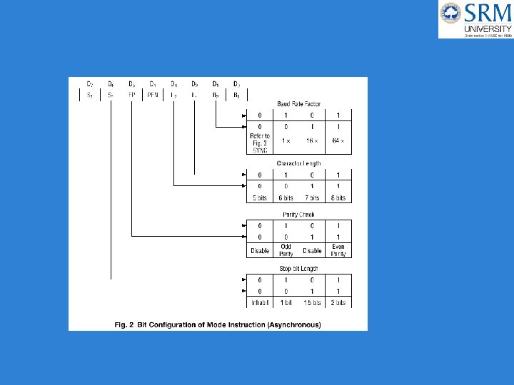
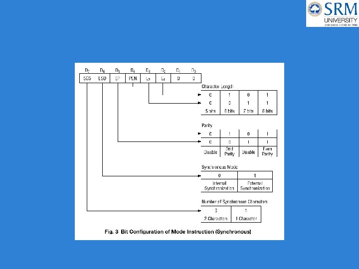
1) Mode Instruction • Mode instruction is used for setting the function of the 8251. Mode instruction will be in "wait for write" at either internal reset or external reset. That is, the writing of a control word after resetting will be recognized as a "mode instruction. " • Items set by mode instruction are as follows: • • Synchronous/asynchronous mode • • Stop bit length (asynchronous mode) • • Character length • • Parity bit • • Baud rate factor (asynchronous mode) • • Internal/external synchronization (synchronous mode) • • Number of synchronous characters (Synchronous mode)
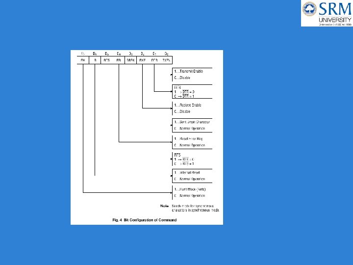
Command • Command is used for setting the operation of the 8251. It is possible to write a command whenever necessary after writing a mode instruction and sync characters. • Items to be set by command are as follows: • • Transmit Enable/Disable • • Receive Enable/Disable • • DTR, RTS Output of data. • • Resetting of error flag. • • Sending to break characters • • Internal resetting • • Hunt mode (synchronous mode)
Status Word