Chapter 10 HCS 12 Serial Peripheral Interface What

? • • • SPI is a synchronous serial")

 • The operating parameters of each SPI module")
")
")
")
")
 • Example 10. 1 Give a value to")
 • The data bits can be shifted on")
")
")
 • • • A mode that uses only one")


 • The HC 595 is often")
 • • Example 10. 5 Describe")


 • Step 1 – Pull the CE")
")


 { char hi_byte, lo_byte, temp, *bptr; unsigned int result; bptr")


 • The MAX 6952 uses eight digit registers to")
 • The data in the digit registers does not")


 • Example 10. 10")
 • • Solution: The")


 Plane P 0 • Display space character and letter")
 Plane P 0 • Display letter U and")
 Plane 0 • Display letters S and C")
 Plane 0 • Display letters M and E on")
; sendtomax(0 x 21, 0 x")


 { char i 1, i 2, i 3, i 4; char")
%40; j 2 = (k+5)%40; j 3 = (k+6)%40; j 4")


 { SPI 0 BR = 0 x 00; SPI 0 CR")
- Slides: 92
Chapter 10 HCS 12 Serial Peripheral Interface
What is Serial Peripheral Interface (SPI)? • • • SPI is a synchronous serial protocol proposed by Motorola to be used as standard for interfacing peripheral chips to a microcontroller. Devices are classified into the master or slaves. The SPI protocol uses four wires to carry out the task of data communication: – – • • MOSI: master out slave in MISO: master in slave out SCK: serial clock SS: slave select An SPI data transfer is initiated by the master device. A master is responsible for generating the SCK signal to synchronize the data transfer. The SPI protocol is mainly used to interface with shift registers, LED/LCD drivers, phase locked loop chips, memory components with SPI interface, or A/D or D/A converter chips.
The HCS 12 SPI Modules • • • An HCS 12 device may have from one to three SPI modules. The MC 9 S 12 DP 256 has three SPI modules: SPI 0, SPI 1, and SPI 2. By default, the SPI 0 share the use of the upper 4 Port S pins: – – • By default, the SPI 1 shares the use of the lower 4 Port P pins: – – • PP 3 SS 1 (can be rerouted to PH 3) PP 2 SCK 1 (can be rerouted to PH 2) PP 1 MOSI 1 (can be rerouted to PH 1) PP 0 MISO 1 (can be rerouted to PH 0) By default, the SPI 2 shares the use of the upper 4 Port P pins: – – • PS 7 SS 0 (can be rerouted to PM 3) PS 6 SCK 0(can be rerouted to PM 5) PS 5 MOSI 0 (can be rerouted to PM 4) PS 4 MISO 0 (can be rerouted to PM 2) PP 6 SS 2 (can be rerouted to PH 7) PP 7 SCK 2(can be rerouted to PH 6) PP 5 MOSI 2 (can be rerouted to PH 5) PP 4 MISO 2 (can be rerouted to PH 4) It is important to make sure that there is no conflict in the use of signal pins when making rerouting decision.
SPI Related Registers (1 of 6) • The operating parameters of each SPI module are controlled via two control registers: – SPIx. CR 1: (x = 0, 1, or 2) – SPIx. CR 2 • • • The baud rate of SPI transfer is controlled by the SPIx. BR register. The operation status of the SPI operation is recorded in the SPIx. SR register. The contents of the SPIx. CR 1, SPIx. CR 2, SPIx. BR, and SPIx. SR registers are illustrated in Figure 10. 1 to 10. 4, respectively. The SS pin may be disconnected from SPI by clearing the SSOE bit in the SPIx. CR 1 register. After that, it can be used as a general I/O pin. If the SSOE bit in the SPIx. CR 1 register is set to 1, then the SS signal will be asserted to enable the slave device whenever a new SPI transfer is started. The equation for setting the SPI baud rate is given in Figure 10. 3.
SPI Related Registers (2 of 6)
SPI Related Registers (3 of 6)
SPI Related Registers (4 of 6)
SPI Related Registers (5 of 6)
SPI Related Registers (6 of 6) • Example 10. 1 Give a value to be loaded to the SPIx. BR register to set the baud rate to 2 MHz for a 24 MHz bus clock. • Solution: 24 MHz 2 MHz = 12. One possibility is to set SPPR 2 -SPPR 0 and SPR 2 -SPR 0 to 010 and 001, respectively. The value to be loaded into the SPIx. BR register is $21. • Example 10. 2 What is the highest possible baud rate for the SPI with 24 MHz bus clock? • Solution: The highest SPI baud rate occurs when both the SPPR 2 -SPPR 0 and SPR 2 -SPR 0 are 000. In this case the baud rate is 24 MH 2 = 12 MHz.
SPI Transmission Format (1 of 3) • The data bits can be shifted on the rising or the falling edge of the SCK clock. • Since the SCK can be idle high or idle low, there are four possible combinations as shown in Figure 10. 5 and 10. 6. • To shift data bits on the rising edge, set CPOL-CPHA to 00 or 11. • To shift data bits on the falling edge, set CPOL-CPHA to 01 or 10. • Data byte can be shifted in and out most significant bit first or least significant bit first.
SPI Transmission Format (2 of 3)
SPI Transmission Format (3 of 3)
Bidirectional Mode (MOMI or SISO) • • • A mode that uses only one data pin to shift data in and out. This mode is provided to deal with peripheral devices with only one data pin. Either the MOSI pin or the MISO pin can be used as the bidirectional pin. When the SPI is configured to the master mode (MSTR bit = 1), the MOSI pin is used in data transmission and becomes the MOMI pin. When the SPI is configured to the slave mode (MSTR bit = 0), the MISO pin is used in data transmission and becomes the SISO pin. The direction of each serial pin depends on the BIDIROE bit of the SPIx. CR 2 register. The pin configuration for MOSI and MISO are illustrated in Figure 10. 7. If one wants to read data from the peripheral device, clear the BIDIROE bit to 0. If one wants to output data to the peripheral device, set the BIDIROE bit to 1. The use of the this mode is illustrated in exercise problem 10. 8.
Mode Fault Error • If the SSx signal goes low while the SPIx is configured as a master, it indicates a system error where more than one master may be trying to drive the MOSIx and SCKx pins simultaneously. • The MODF bit in the SPIx. SR register will be set to 1 when mode fault condition occurs. • When mode fault occurs, the MSTR bit will be cleared to 0 and the output enable for the MOSIx and SCKx pins will be deasserted.
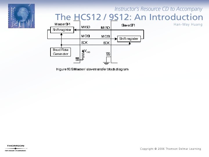
SPI Circuit Connection • In an SPI system, one device is configured as a master. Other devices are configured as slaves. • The circuit connection for a single-slave system is shown in Figure 10. 8. • A multi-slave system may have two different connection methods as illustrated in Figure 10. 9 and 10. • In Figure 10. 9, the master can exchange data with each individual slave without affecting other slaves. • In Figure 10. 10, all the slaves are configured into a larger ring. A data transmission with certain slaves will go through other slaves.
• Example 10. 3 Configure the SPI 0 to operate with the following setting assuming that E • clock is 24 MHz: – – – – 6 MHz baud rate Enable SPI 0 to master mode SCK 0 pin idle low with data shifted on the rising edge of SCK Transfer data most significant bit first and disable interrupt Disable SS 0 function Stop SPI in Wait mode Normal SPI operation (not bidirectional mode)
• Solution: f. E / baud rate = 24 MHz/6 MHz = 4. We need to set SPPR 2 -SPPR 0 and SPR 2 -SPR 0 to 001 and 000, respectively. Write the value $10 into the SPI 0 BR register. – The following instruction sequence will configure the SPI 0 as desired: movb #$10, SPI 0 BR movb #$50, SPI 0 CR 1 movb #$02, SPI 0 CR 2 movb #0, WOMS ; set baud rate to 6 MHz ; disable interrupt, enable SPI, SCK idle low, data ; latched on rising edge, data transferred msb first ; disable bidirectional mode, stop SPI in wait mode ; enable Port S pull-up
SPI Utility Functions • The following operations are common in many applications and should be made into library functions to be called by many SPI applications: – – Send a character to SPI Send a string to SPI Read a character from SPI Read a string from SPI putcspix (x = 0, 1, or 2) putsspix (x = 0, 1, or 2) getcspix (x = 0, 1, or 2) getsspix (x = 0, 1, or 2)
Function putc. SPI 0 putcspi 0 brclr staa brclr ldaa rts SPI 0 SR, SPTEF, * SPI 0 DR SPI 0 SR, SPIF, * SPI 0 DR void putcspi 0 (char cx) { char temp; while(!(SPI 0 SR & SPTEF)); SPI 0 DR = cx; while(!(SPI 0 SR & SPIF)); temp = SPI 0 DR; } ; wait until write operation is permissible ; output the character to SPI 0 ; wait until the byte is shifted out ; clear the SPIF flag /* wait until write is permissible */ /* output the byte to the SPI */ /* wait until write operation is complete */ /* clear the SPIF flag */
Function puts. SPI 0 ; the string to be output is pointed to by X putsspi 0 ldaa 1, x+ ; get one byte to be output to SPI port beq doneps 0 ; reach the end of the string? jsr putcspi 0 ; call subroutine to output the byte bra putsspi 0 ; continue to output doneps 0 rts void putsspi 0(char *ptr) { while(*ptr) { /* continue until all characters have been output */ putcspi 0(*ptr); ptr++; } }
Function getc. SPI 0 ; This function reads a character from SPI 0 and returns it in accumulator A getcspi 0 brclr staa brclr ldaa rts SPI 0 SR, SPTEF, * ; wait until write operation is permissible SPI 0 DR ; trigger eight clock pulses for SPI transfer SPI 0 SR, SPIF, * ; wait until a byte has been shifted in SPI 0 DR ; return the byte in A and clear the SPIF flag char getcspi 0(void) { while(!(SPI 0 SR & SPTEF)); SPI 0 DR = 0 x 00; while(!(SPI 0 SR & SPIF)); return SPI 0 DR; } /* wait until write is permissible */ /* trigger 8 SCK pulses to shift in data */ /* wait until a byte has been shifted in */ /* return the character */
Function gets. SPI 0 ; This function reads a string from the SPI and store it in a buffer pointed to by X ; The number of bytes to be read in passed in accumulator B getsspi 0 tstb beq jsr staa decb bra donegs 0 clr rts donegs 0 getcspi 0 1, x+ getsspi 0 0, x ; check the byte count ; return when byte count is zero ; call subroutine to read a byte ; save the returned byte in the buffer ; decrement the byte count ; terminate the string with a NULL character void getsspi 0(char *ptr, char count) { while(count) { /* continue while byte count is nonzero */ *ptr++ = getcspi 0(); /* get a byte and save it in buffer */ count--; } *ptr = 0; /* terminate the string with a NULL */ }
The HC 595 Shift Register • The HC 595 consists of an 8 -bit shift register and a D-type latch with three-state parallel output. • The shift register provides parallel data to the latch. • The maximum data shift rate is 100 MHz (Philips part).
Signal Pins of the HC 595 • DS: serial data input • SC: shift clock. A low-to-high transition on this pin causes the data at the serial input pin to be shifted into the 8 -bit shift register. • Reset: A low on this pin resets the shift register portion of this device. • LC: latch clock. A low-to-high transition on this pin loads the contents of the shift register into the output latch. • OE: output enable. A low on this pin allows the data from the latches to be presented at the outputs. • QA to QH: tri-state latch output • SQH: the output of the eight stage of the shift register
Applications of the HC 595 (1 of 2) • The HC 595 is often used to add parallel ports to the microcontroller. • Both the connection methods shown in Figure 10. 9 and 10. 10 can be used to add parallel ports to the MCU.
Applications of the HC 595 (2 of 2) • • Example 10. 5 Describe how to use two 74 HC 595 s to drive eight common cathode seven-segment displays assuming that the E clock frequency of the HCS 12 is 24 MHz. Solution: Use the circuit in figure 10. 12 to connect two 74 HC 595 s to the HCS 12.
Program to display 87654321 on display #7 to #0 #include “c: miniidehcs 12. inc" org $1000 icnt ds. b 1 org $1500 lds #$1500 bset DDRK, $80 jsr openspi 0 forever ldx #disp. Tab movb #8, icnt loop ldaa 1, x+ jsr putcspi 0 bclr PTK, BIT 7 bset PTK, BIT 7 ldy #1 jsr delayby 1 ms dec icnt bne loop bra forever ; loop count ; set up stack pointer ; configure the PK 7 pin for output ; configure SPI 0 ; use X as a pointer to the table ; set loop count to 8 ; send the digit select byte to the 74 HC 595 ; " ; send segment pattern to 74 HC 595 ; " ; transfer data from shift register to output ; latch ; display the digit for one ms ; " ; ; if not reach digit 1, then next ; start from the start of the table
openspi 0 movb #0, SPI 0 BR ; set baud rate to 12 MHz movb #$50, SPI 0 CR 1 ; disable interrupt, enable SPI, SCK idle low, ; latch data on rising edge, transfer data msb first movb #$02, SPI 0 CR 2 ; disable bidirectional mode, stop SPI in wait mode movb #0, WOMS ; enable Port S pull-up rts #include "c: miniidedelay. asm" #include "c: miniidespi 0 util. asm" ; ********************************** ; Each digit consists of two bytes of data. The first byte is ; digit select, the second byte is the digit pattern. ; ********************************** disp. Tab dc. b $80, $7 F, $40, $70, $20, $5 F, $10, $5 B dc. b $08, $33, $04, $79, $02, $6 D, $01, $30 end
#include “c: egnu 091includehcs 12. h” #include “c: egnu 091includespi 0 util. c” #include “c: egnu 091includedelay. c” void openspi 0(void); void main (void) { unsigned char disp_tab[8][2] = {{0 x 80, 0 x 7 F}, {0 x 40, 0 x 70}, {0 x 20, 0 x 5 F}, {0 x 10, 0 x 5 B}, {0 x 08, 0 x 33}, {0 x 04, 0 x 79}, {0 x 02, 0 x 6 D}, {0 x 01, 0 x 30}}; char i; openspi 0(); /* configure the SPI 0 module */ DDRK |= BIT 7; /* configure pin PK 7 as output */ while(1) { for (i = 0; i < 8; i++) { putcspi 0(disp_tab[i][0]); /* send out digit select value */ putcspi 0(disp_tab[i][1]); /* send out segment pattern */ PTK &= ~BIT 7; /* transfer values to latches of 74 HC 595 s */ PTK |= BIT 7; /* " */ delayby 1 ms(1); /* display a digit for 1 ms */ } } }
The TC 72 Digital Thermometer • • • 10 -bit resolution and SPI interface Pin assignment and block diagram shown in Figure 10. 13. Capable of reading temperature from -55 o. C to 125 o. C. Can be used in continuous temperature conversion or one-shot conversion mode. Has internal clock generator to control the automatic temperature conversion sequence
Temperature Data Format • Temperature is represented by a 10 -bit two’s complement word with a resolution of 0. 25 o. C per least significant bit. • The converter is scaled from -128 o. C to +127 o. C with 0 o. C represented as 0 x 0000. • The temperature value is stored in two 8 -bit registers. • Whenever the most significant bit is 1, the temperature is negative. • A sample of temperature reading is shown.
TC 72’s Serial Interface • • The CE input to the TC 72 must be asserted (high) to enable SPI transfer. Data can be shifted on the rising edge or the falling edge depending on the idle polarity of the SCK source. Data transfer to and from the TC 72 consists of one address byte followed by one or multiple data (2 to 4) bytes. The TC 72 registers and their addresses are shown in Table 10. 4. The most significant bit of the address byte determines whether a read (A 7 = 0) or a write (A 7 = 1) operation will occur. A multiple byte read operation will start from high address toward lower addresses. The user can send in the temperature result high byte address and read the temperature result high byte, low byte, and the control registers.
Procedure for Reading Temperature (1 of 2) • Step 1 – Pull the CE pin high to enable SPI transfer. • Step 2 – Send the temperature result high byte read address (0 x 02) to the TC 72. Wait until the SPI transfer is complete. • Step 3 – Read the temperature result high byte. The user needs to write a dummy byte into the SPI data register to trigger eight clock pulses. • Step 4 – Read the temperature result low byte. Again, the user needs to write a dummy byte into the SPI data register to trigger eight clock pulses. • Step 5 – Pull CE pin to low so that a new transfer can be started. • Single-byte read and multiple-byte read timing diagrams are shown in Figures 10. 15 b and 10. 15 c.
Procedure for Reading Temperature (2 of 2)
Control Register • • • The control register is used to select the shutdown, continuous, or one-shot conversion operating mode. The temperature conversion mode selection logic is shown in Table 10. 5. At power up, the SHDN bit is 1. Thus the TC 72 is in the shutdown mode. If the SHDN bit is 0, the TC 72 will perform a temperature conversion approximately every 150 ms. A temperature conversion will be initiated by a write operation into the control register to select the continuous mode or one-shot mode. A typical circuit connection between the TC 72 and the HCS 12 is shown in Figure 10. 16.
• Example 10. 6 Write a C program to read the temperature every 200 ms. Convert the temperature to a string so that it can be displayed in an appropriate output device. A pointer to hold the string will be passed to this function. The bus clock is 24 MHz.
#include “c: egnu 091includehcs 12. h” #include “c: egnu 091includespi 0 util. c” #include “c: egnu 091includedelay. c” #include “c: egnu 091includeconvert. c” void read_temp (char *ptr); void openspi 0(void); char buf[10]; void main (void) { DDRM |= BIT 1; /* configure the PM 1 pin for output */ openspi 0(); /* configure SPI 0 module */ read_temp(&buf[0]); } void openspi 0(void) { SPI 0 BR = 0 x 10; /* set baud rate to 6 MHz */ SPI 0 CR 1 = 0 x 50; /* enable SPI 0 to master mode, select rising edge to shift data in and out */ SPI 0 CR 2 = 0 x 02; /* select normal mode and stop SPI in wait mode */ WOMS = 0 x 00; /* enable Port S pull-up */ }
void read_temp (char *ptr) { char hi_byte, lo_byte, temp, *bptr; unsigned int result; bptr = ptr; PTM |= BIT 1; /* enable TC 72 data transfer */ putcspi 0(0 x 80); /* send out TC 72 control register write address */ putcspi 0(0 x 11); /* perform one shot conversion */ PTM &= ~BIT 1; /* disable TC 72 data transfer */ delayby 100 ms(2); /* wait until temperature conversion is complete */ PTM |= BIT 1; /* enable TC 72 data transfer */ putcspi 0(0 x 02); /* send MSB temperature read address */ hi_byte = getcspi 0(); /* read the temperature high byte */ lo_byte = getcspi 0(); /* save temperature low byte and clear SPIF */ PTM &= ~BIT 1; /* disable TC 72 data transfer */ lo_byte &= 0 x. C 0; /* make sure the lower 6 bits are 0 s */ result = (int) hi_byte * 256 + (int) lo_byte; if (hi_byte & 0 x 80) { /* temperature is negative */ result = ~result + 1; /* take the two' complement of result */ result >>= 6;
temp = result & 0 x 0003; /* place the lowest two bits in temp */ result >>= 2; /* get rid of fractional part */ *ptr++ = 0 x 2 D; /* store the minus sign */ int 2 alpha(result, ptr); } else { /* temperature is positive */ result >>= 6; temp = result & 0 x 0003; /* save fractional part */ result >>= 2; /* get rid of fractional part */ int 2 alpha(result, ptr); /* convert to ASCII string */ } while(*bptr){ /* search the end of the string */ bptr++; }; switch (temp){ /* add fractional digits to the temperature */ case 0: break; case 1: /* fractional part is. 25 */ *bptr++ = 0 x 2 E; /* add decimal point */ *bptr++ = 0 x 32; *bptr++ = 0 x 35; *bptr = '�'; break;
case 2: /* fractional part is. 5 */ *bptr++ = 0 x 2 E; /* add decimal point */ *bptr++ = 0 x 35; *bptr = '�'; break; case 3: /* fractional part is. 75 */ *bptr++ = 0 x 2 E; /* add decimal point */ *bptr++ = 0 x 37; *bptr++ = 0 x 35; *bptr = '�'; break; default: break; } }
The D/A Converter TLV 5616 • • The TLV 5616 is a 12 -bit voltage output digital-to-analog converter (DAC) with SPI interface. The TLV 5616 has an output settling time of 3 ms in fast mode and 9 ms in slow mode. A D/A conversion is started by writing a 16 -bit serial string that contains 4 control bits and 12 data bits to the TLV 5616 can operate from 2. 7 V to 5. 5 V.
TLV 5616 Signal Pins • • AGND: CS: DIN: FS: OUT: REFIN: SCLK: VDD: analog ground chip select (active low) serial data input frame sync DAC analog output reference analog input voltage serial clock input positive power supply
Date Format - A 16 -bit frame with 4 control bits and 12 data bits.
TLV 5616 Output Voltage • The output voltage is given by the following expression: – VOUT = 2 REF code 2 n • The reference voltage input cannot be higher than VDD/2.
Data Shifting Timing • The FS pulse must be generated before data shifting can start. • The highest data shift rate is 20 MHz.
CS and FS Trigger Sequence • • Pull FS to high. Pull CS to low. Pull FS to low. Send out control and data bits using the SPI transfer. • Wait until all 16 bits have been shifted out; pull FS to high. • Pull CS to high.
Circuit Connection between the TLV 5616 and HCS 12
• Example 10. 9 Write a program to generate a waveform that is a repetition of the waveform shown in Figure 10. 21 using the circuit shown in Figure 10. 20. • The values to be sent to the TLV 5616 to generate 0 V, 1 V, 2 V, and 3 V outputs are: val(0) = 0 val(1) = 212/4 = 1024 val(2) = 2 212/4 = 2048 val(3) = 3 212/4 = 3072 • The 16 -bit values (in fast mode) to be written to the TLV 5616 for this four voltages are as follows: code (0) = $4000 code (1) = $4400 code (2) = $4800 code (3) = $4 C 00
#include PM 7 PM 6 prolog epilog forever iloop "c: miniidehcs 12. inc" equ BIT 7 equ BIT 6 macro bset PTM, PM 7 bclr PTM, PM 6 bclr PTM, PM 7 endm macro bset PTM, PM 7 bset PTM, PM 6 endm org lds bset jsr ldx ldab prolog ldaa $1500 #$1500 DDRM, $C 0 openspi 0 #D 2 ATab #8 1, x+ ; pull FS to high ; pull CS to low ; pull FS to high ; pull CS to high ; set up the stack pointer ; configure the PM 6 and PM 7 pins for output ; configure SPI 0 properly ; Use X to point to the table ; entry count set to 8 ; activate an FS pulse and pull CS to low ; output 0 V from OUT pin
D 2 ATab openspi 0 #include jsr putcspi 0 ; " ldaa 1, x+ ; " jsr putcspi 0 ; " epilog ; pull PM 7 and PM 6 to high ldy #1 ; wait for 1 ms jsr delayby 1 ms ; " dbne b, iloop ; reach the end of the table? bra forever ; yes, start from the beginning dc. b $40, $00, $44, $00, $48, $00, $44, $00 dc. b $48, $00, $44, $00, $48, $00, $4 C, $00 movb #0, SPI 0 BR ; set baud rate to 12 MHz movb #$54, SPI 0 CR 1 movb #$02, SPI 0 CR 2 movb #0, WOMS ; enable Port S pull-up rts "c: miniidedelay. asm" "c: miniidespi 0 util. asm" end
Matrix LED Displays • Many organizations have the need to display important information at the entrance or some corners of their buildings. • The information to be displayed can be rotated. • Common matrix LED displays format are 5 7, 5 8, and 8 8. • One can find color matrix LEDs with red, green, and red color. • Matrix LED displays can be organized as cathode-row or anode-row. • All LEDs in a cathode-row matrix LED display have a common cathode whereas those in anode-row matrix LED display have a common anode.
The Driving Method of Matrix LED Displays • Two parallel ports are needed to drive the matrix display. • One port drives the column whereas the other port drives the rows. • One needs to scan the matrix LED displays one row at a time, from top to bottom. • For multiple matrix LED displays in the application, timemultiplexing technique needs to be used. • Dedicated driver chips such as MAX 6952 (SPI interface) and MAX 6953 (I 2 C interface) are available for cathoderow matrix LED displays to simplify the interfacing.
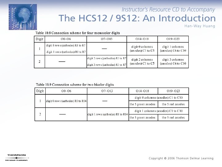
The MAX 6952 Matrix Display Driver • Designed to drive cathode-row matrix displays with 5 7 organization • Can operate with power supply from 2. 7 V to 5. 5 V • Can drive four monocolor or two bicolor cathode-row matrix displays • Has built-in 104 -character Arial font and 24 user definable characters • Allows automatic blinking control for each segment and provides 16 -step digital brightness control • Pin functions shown in Table 10. 7 • Pin connections illustrated in Table 10. 8 and 10. 9
One MAX 6952 Drives Four Matrix Displays
Concatenation of Multiple MAX 6952 s • Multiple MAX 6952 s can be concatenated to drive more than four matrix displays.
MAX 6952 Block Diagram
Procedure for Writing the MAX 6952 • Step 1 – Pull the CLK signal to low. • Step 2 – Pull the CS signal to low to enable the internal 16 -bit shift register. • Step 3 – Shift in 16 bits of data from the DIN pin with the most significant bit first. The most significant bit (D 15) must be low for a write operation. • Step 4 – Pull the CS signal to high. • Step 5 – Pull the CLK to low.
Procedure for Reading the MAX 6952 Register • Step 1 – Pull the CLK signal to low. • Step 2 – Pull the CS signal to low to enable SPI transfer. • Step 3 – Clock 16 bits into the DIN pin with bit 15 first. Bit 15 must be a 1. Bits 14 to 8 contain the address of the register to be read. Bits 7 to 0 contain dummy data. • Step 4 – Pull the CS signal to high. Bits 7 to of the shift register will be loaded with the data in the register addressed by bits 15 through 8. • Step 5 – Pull CLK to low. • Step 6 – Issue another read command examine the bit stream at the DOUT pin. The second 8 bits are the contents of the register addressed by bits 14 to 8 in Step 3.
MAX 6952 Register Map
Digit Registers (1 of 2) • The MAX 6952 uses eight digit registers to store the characters that the user wishes to display on the four 5 7 digits. • These digit registers are placed in two planes (P 0 and P 1) with each plane having 4 bytes. • Each LED digit is represented by 2 bytes of memory, one byte in plane P 0 and the other in plane P 1. • A digit data can be updated in P 0, or P 1, or both at the same time as shown in Table 10. • If the blink function is disabled, then the digit register data in plane P 0 is used to multiplex the display. • If the blink function is enabled, then the digit register data in both plane P 0 and P 1 are alternately used to multiplex the display. • Blinking is achieved by multiplexing the LED display using data planes P 0 and P 1 on alternate phases of the blink clock. The multiplexing pattern in shown in Table 10. 11.
Digit Registers (2 of 2) • The data in the digit registers does not control the digit segments directly. • The register data is used to address a character generator, which stores the data of a 128 -character font. • The lower 7 bits of he display data select the character font. • The bit 7 of the register data selects whether the font data is used directly (D 7 = 0) or whether the font is inverted (D 7 = 1).
Configuration Register • The configuration register is used to enter and exit shutdown, select the blink rate, enable and disable the blink function, clear the digit data, and reset the blink timing.
Intensity Registers • Display brightness is controlled by four pulse-width modulators, one for each display digit. • The upper four bits of the Intensity 10 register control the intensity of the matrix display 1, whereas the lower four bits of the same register control the brightness of the display 0. • Matrix display digits 3 and 2 are controlled by the upper four bits and lower four bits of the Intensity 32 register, respectively. • The modulator scales the average segment current in 16 steps from a maximum of 15/16 down to 1/16 of the peak current.
Scan Limit Register • This register allows the user to choose between displaying two or four matrix displays. • The multiplexing scheme drives digits 0 and 1 at the same time, then digits 2 and 3 at the same time.
Scan Test Register • This register switches the drivers between two modes: normal and test. • Display test mode turns on all LEDs by overriding, but not altering all control and digit registers. • In display test mode, eight digits are scanned and the duty cycle is 7/16 (half power).
Character Generator Font Mapping • The character generator comprises 104 characters in ROM, and 24 user-definable characters. ` • The lower 7 bits of the digit register select the character fonts. • The character map follows the Arial font for 96 characters in the range from %0101000 to %1111111. • The first 32 characters map the 24 user-defined positions (RAM 00 to RAM 23), plus eight extra common characters in ROM. • When the msb is 0 the device will display the font normally. Otherwise, the chip will display the font inversely.
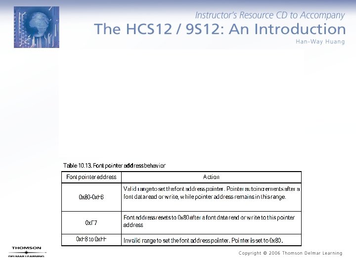
User-Defined Font Register • • The 24 user-definable characters are represented by 120 entries of 7 -bit data, five entries per character in the SRAM. The 120 user definable font data are written and read through a single register at the address 0 x 05. An auto-incrementing font address pointer indirectly accesses the font data. The font data is written to and read from the MAX 6952 indirectly, using the font address pointer. To define user fonts, the user first needs to set the font address pointer. This is done by placing the address in the font address pointer register and set the bit 7 to 1. After this, one can write the font data to the lower 7 bits and clear the bit 7. The font address pointer autoincrements after a valid access to the user-defined font data. The memory mapping of user-defined font register 0 x 05 is detailed in Table 10. 12. The behavior of the font pointer address is illustrated in Table 10. 13. To display the user-defined fonts, one must send in the RAM address from 0 x 00 to 0 x 17, corresponding to the font address pointer value that is 5 RAM address.
Blinking Operation • The blinking operation makes the LED drivers flip between displaying the digit register data in planes P 0 and P 1. • If the digit register data for any digit is different in two planes, then that digit appears to flip between two characters. • To make a character to appear to blink on and off, write the character to one plane and use the blank character for the other plane. • Blinking is enabled by setting the E bit of the configuration register. • The blink speed can be programmed to be fast or slow and is determined by the frequency of the multiplex clock, OSC, and by setting the B bit of the configuration register.
Choosing Values for RSET and CSET • The MAX 6952 uses an RC oscillator to generate clock signals for display multiplexing. • The recommended RSET and CSET values are 53. 6 K and 26 p. F, respectively. • The recommended values for RSET and CSET will set the slow and fast blinking frequencies to 0. 5 Hz and 1 Hz. • The recommended values for RSET and CSET will set the peak current to 40 m. A.
The Circuit that Daisy-Chains Two MAX 6952 (1 of 2) • Example 10. 10 Connect eight matrix displays to these MAX 6952 driver chips. Assume that the E clock frequency is 24 MHz. Write a program to configure the SPI function to shift data at 12 MHz and display the string “MSU ECET”.
The Circuit that Daisy-Chains Two MAX 6952 (2 of 2) • • Solution: The SPI 0 module should be configured with the following setting: – 12 MHz baud rate – Master mode with interrupts disabled – Shift data on the rising edge with clock idle low – Shift data out most significant bit first – Disable mode fault – Stop SPI 0 in wait mode • The setting of two MAX 6952 s are as follows: – Intensity 10 registers • Set to maximum intensity • Send the values 0 x 01, 0 x. FF, 0 x 01, and 0 x. FF to these two registers. – Intensity 32 registers • Set to maximum intensity • Send the values 0 x 02, 0 x. FF, 0 x 02, and 0 x. FF to these two registers – Scan limit registers • Drive four monocolor matrix displays • Send the values 0 x 03, 0 x 01, 0 x 03, and 0 x 01 to these two registers
Configuration Registers • • Select P 1 blink phase Not to clear digit data on both plane P 1 and P 0 Reset blink counter on the rising edge of CS Disable blink function Select slow blinking (doesn’t matter) Select normal mode Send the values 0 x 04, 0 x 11, 0 x 04, and 0 x 11 to these two registers
Display Test Registers • Disable test. • Send the values 0 x 07, 0 x 00, 0 x 07, and 0 x 00 to these two registers.
Digit 0 Registers (Rightmost Digit) Plane P 0 • Display space character and letter T on he display 0 of the first and second MAX 6952. • Send the values 0 x 20, 0 x 54, 0 x 20, and 0 x 20 to these two registers.
Digit 1 registers (second rightmost digit) Plane P 0 • Display letter U and E on the display 1 of the 1 st and 2 nd MAX 6952. • Send the values 0 x 21, 0 x 45, 0 x 21, and 0 x 55 to these two registers.
Digit 2 Registers (Second Leftmost Digit) Plane 0 • Display letters S and C on the display 2 of the 1 st and 2 nd MAX 6952. • Send the values 0 x 22, 0 x 43, 0 x 22, and 0 x 53 to these registers.
Digit 3 Registers (Leftmost Digit) Plane 0 • Display letters M and E on the display 3 of the 1 st and 2 nd MAX 6952. • Send the values 0 x 23, 0 x 45, 0 x 23, and 0 x 4 D to these registers. – The program that perform the desired configuration is as follows: #include “c: egnu 091includehcs 12. h” #include “c: egnu 091includespi 0 util. c” void sendtomax(char x 1, char x 2, char x 3, char x 4); void openspi 0(void); void main (void) { openspi 0(); DDRM |= BIT 5; // configure PM 5 pin for output sendtomax(0 x 01, 0 x. FF, 0 x 01, 0 x. FF); // set intensity for digits 0 & 1 sendtomax(0 x 02, 0 x. FF, 0 x 02, 0 x. FF); // set intensity for digits 2 & 3 sendtomax(0 x 03, 0 x 01, 0 x 03, 0 x 01); // set scan limit to drive 4 digits sendtomax(0 x 04, 0 x 11, 0 x 04, 0 x 11); // set configuration register sendtomax(0 x 07, 0 x 00, 0 x 07, 0 x 00); // disable test
sendtomax(0 x 20, 0 x 54, 0 x 20); sendtomax(0 x 21, 0 x 45, 0 x 21, 0 x 55); sendtomax(0 x 22, 0 x 43, 0 x 22, 0 x 53); sendtomax(0 x 23, 0 x 45, 0 x 23, 0 x 4 D); // value for digit 0 // value for digit 1 // value for digit 2 // value for digit 3 } void sendtomax (char c 1, char c 2, char c 3, char c 4) { char temp; PTM &= ~BIT 5; /* enable SPI transfer to MAX 6952 */ putcspi 0(c 1); /* send c 1 to MAX 6952 */ putcspi 0(c 2); /* send c 2 to MAX 6952 */ putcspi 0(c 3); /* send c 3 to MAX 6952 */ putcspi 0(c 4); /* send c 4 to MAX 6952 */ PTM |= BIT 5; /* load data from shift register to latch */ } void openspi 0(void) { SPI 0 BR = 0 x 00; /* set baud rate to 12 MHz */ SPI 0 CR 1 = 0 x 50; /* disable interrupt, set master mode, shift data on rising edge, clock idle low */ SPI 0 CR 2 = 0 x 02; /* disable mode fault, disable SPI in wait mode */ WOMS = 0; /* enable Port S pull-up */ }
• • Example 10. 11 Modify the previous example to blink the display at a slow rate. Solution: The setting of the configuration needs to be changed and we need to send the space character (0 x 20) to the plane P 1. Send the values 0 x 04, 0 x 19, 0 x 03, and 0 x 19 to the configuration registers. void main (void) { openspi 0(); DDRM |= BIT 5; sendtomax(0 x 01, 0 x. FF, 0 x 01, 0 x. FF); sendtomax(0 x 02, 0 x. FF, 0 x 02, 0 x. FF); sendtomax(0 x 03, 0 x 01, 0 x 03, 0 x 01); sendtomax(0 x 04, 0 x 19, 0 x 04, 0 x 19); sendtomax(0 x 07, 0 x 00, 0 x 07, 0 x 00); sendtomax(0 x 20, 0 x 54, 0 x 20); sendtomax(0 x 21, 0 x 45, 0 x 21, 0 x 55); sendtomax(0 x 22, 0 x 43, 0 x 22, 0 x 53); sendtomax(0 x 23, 0 x 45, 0 x 23, 0 x 4 D); sendtomax(0 x 40, 0 x 20, 0 x 40, 0 x 20); sendtomax(0 x 41, 0 x 20, 0 x 41, 0 x 20); sendtomax(0 x 42, 0 x 20, 0 x 42, 0 x 20); sendtomax(0 x 43, 0 x 20, 0 x 43, 0 x 20); } // configure PM 5 pin for output // configuration register, blink at phase P 1 // disable test // value for digit 0 on plane P 0 // value for digit 1 // value for digit 2 // value for digit 3 // value for digit 0 on plane P 1 (space) // value for digit 1 “ // value for digit 2 “ // value for digit 3 “
• Example 10. 12 For the circuit shown in Figure 10. 30, write a program to display the following message and shift the information from right-to-left every second and enable blinking: 08: 30: 40 Wednesday, 72 o. F, humidity: 60% • Solution: One possible solution is as follows: – Use the plane P 0 to shift the message once every half a second. – Use the message in plane P 0 to multiplex the displays in half a second. – Use the message sent to the plane P 1 to multiplex the displays in the next half of a second. – Display space characters in plane P 1 only to create blinking effect. – Use a delay function to control the shifting of the message. #include “c: egnu 091includehcs 12. h” #include “c: egnu 091includespi 0 util. c” #include “c: egnu 091includedelay. c” void send 2 max (char x 1, char x 2, char x 3, char x 4); void openspi 0 (void); char msg. P 0[41] = "08: 30: 40 Wednesday, 72 o. F, humidity: 60% ";
void main (void) { char i 1, i 2, i 3, i 4; char j 1, j 2, j 3, j 4; char k; openspi 0(); DDRM |= BIT 5; // configure PM 5 pin for output send 2 max(0 x 01, 0 x. FF, 0 x 01, 0 x. FF); send 2 max(0 x 02, 0 x. FF, 0 x 02, 0 x. FF); send 2 max(0 x 03, 0 x 01, 0 x 03, 0 x 01); send 2 max(0 x 04, 0 x 1 D, 0 x 04, 0 x 1 D); // configuration register send 2 max(0 x 40, 0 x 20, 0 x 40, 0 x 20); // send space character to plane P 1 send 2 max(0 x 41, 0 x 20, 0 x 41, 0 x 20); send 2 max(0 x 42, 0 x 20, 0 x 42, 0 x 20); send 2 max(0 x 43, 0 x 20, 0 x 43, 0 x 20); k = 0; while (1) { i 1 = k; i 2 = (k+1)%40; i 3 = (k+2)%40; i 4 = (k+3)%40;
j 1 = (k+4)%40; j 2 = (k+5)%40; j 3 = (k+6)%40; j 4 = (k+7)%40; sendtomax(0 x 20, msg. P 0[i 1], 0 x 20, msg. P 0[j 1]); sendtomax(0 x 21, msg. P 0[i 2], 0 x 21, msg. P 0[j 2]); sendtomax(0 x 22, msg. P 0[i 3], 0 x 22, msg. P 0[j 3]); sendtomax(0 x 23, msg. P 0[i 4], 0 x 23, msg. P 0[j 4]); delayby 100 ms(10); /* wait for 1 s */ k = (k+1)%40; } } void sendtomax (char c 1, char c 2, char c 3, char c 4) { PTM &= ~BIT 5; /* enable SPI transfer to MAX 6952 */ putcspi 0(c 1); /* send c 1 to MAX 6952 */ putcspi 0(c 2); /* send c 2 to MAX 6952 */ putcspi 0(c 3); /* send c 3 to MAX 6952 */ putcspi 0(c 4); /* send c 4 to MAX 6952 */ PTM |= BIT 5; /* load data from shift register to latch */ }
• Example 10. 13 Write a program to define fonts for three special characters as shown below. Store these three special characters’ font at locations from 0 x 00 to 0 x 0 E of the MAX 6952.
#include “c: egnu 091includehcs 12. h” #include “c: egnu 091includespi 0 util. c” char fonts [15] = {0 x 70, 0 x 40, 0 x 7 F, 0 x 40, 0 x 70, 0 x 48, 0 x 38, 0 x 0 F, 0 x 38, 0 x 49, 0 x 7 F, 0 x 49}; void send_font (char xc); void openspi 0 (void); void main (void) { char i; DDRM |= BIT 5; /* configure PM 5 pin for output */ openspi 0(); /* configure SPI module properly */ send_font(0 x 80); /* set font address pointer address to 0 x 00 */ for (i = 0; i < 15; i++) send_font(fonts[i]); } void send_font(char xx) { PTM &= ~BIT 5; /* enable SPI transfer */ putcspi 0(0 x 05); /* specify font address pointer */ putcspi 0(xx); /* send a font value */ PTM |= BIT 5; /* load data in shift register to destination */ }
void openspi 0(void) { SPI 0 BR = 0 x 00; SPI 0 CR 1 = 0 x 50; SPI 0 CR 2 = 0 x 02; WOMS = 0; /* set baud rate to 12 MHz */ /* disable interrupt, set master mode, shift data on rising edge, clock idle low */ /* disable mode fault, disable SPI in wait mode */ /* enable Port S pull-up */ } The statements to display those three Chinese characters followed by letters A, B, C, D, and E from left to right on the matrix LED displays shown in Figure 10. 30 are as follows: sendtomax(0 x 20, 0 x 42, 0 x 20, 0 x 00); // 0 x 00 is the address of the first character font sendtomax(0 x 21, 0 x 43, 0 x 21, 0 x 01); // 0 x 01 is the address of the second character font sendtomax(0 x 22, 0 x 44, 0 x 22, 0 x 02); // 0 x 02 is the address of the third character font sendtomax(0 x 23, 0 x 45, 0 x 23, 0 x 41);