CHAPTER 4 Introduction to Shift Register By Pn
CHAPTER 4 Introduction to Shift Register By : Pn Siti Nor Diana Ismail
Register • A register is a memory device that can be used to store more than one-bit information • A register is usually realized as several flip-flops with common control signals that control the movement of data to and from the register. (shifting data 1 s and 0 s) • A register can consist of one or more FF is used to store and shift data. • A register in digital circuit with 2 basic function : data storage and data movement
Basic Shift Register Function Shift Register consists of an arrangement of Flip-flop. Important in applications involving storage and transfer data in digital system. Has no specified sequence of states. D flip-flop is used
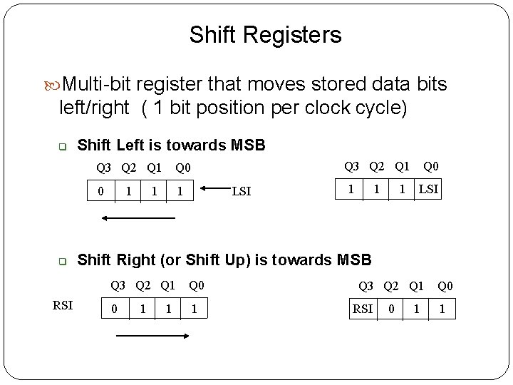
Shift Registers Multi-bit register that moves stored data bits left/right ( 1 bit position per clock cycle) RSI Shift Left is towards MSB Q 3 Q 2 Q 1 Q 0 0 1 1 1 Q 3 Q 2 Q 1 LSI 1 1 1 Q 0 LSI Shift Right (or Shift Up) is towards MSB Q 3 Q 2 Q 1 Q 0 0 1 1 1 Q 3 Q 2 Q 1 RSI 0 1 Q 0 1
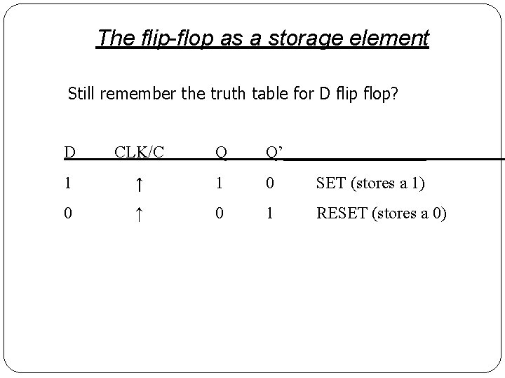
The flip-flop as a storage element Still remember the truth table for D flip flop? D CLK/C Q Q’_________ 1 ↑ 1 0 SET (stores a 1) 0 ↑ 0 1 RESET (stores a 0)
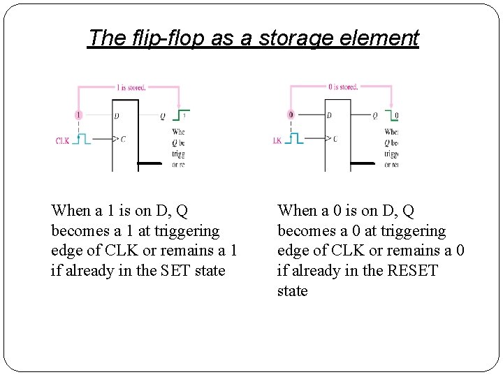
The flip-flop as a storage element When a 1 is on D, Q becomes a 1 at triggering edge of CLK or remains a 1 if already in the SET state When a 0 is on D, Q becomes a 0 at triggering edge of CLK or remains a 0 if already in the RESET state
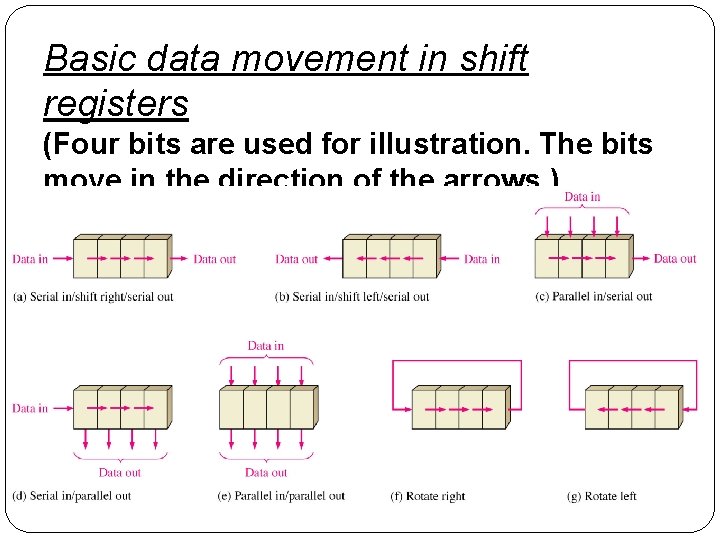
Basic data movement in shift registers (Four bits are used for illustration. The bits move in the direction of the arrows. )
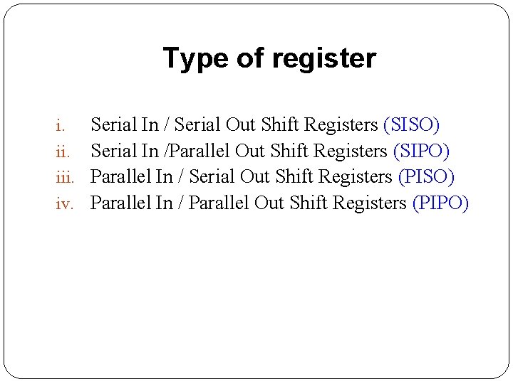
Type of register Serial In / Serial Out Shift Registers (SISO) ii. Serial In /Parallel Out Shift Registers (SIPO) iii. Parallel In / Serial Out Shift Registers (PISO) iv. Parallel In / Parallel Out Shift Registers (PIPO) i.
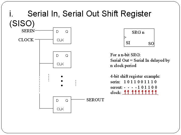
i. Serial In, Serial Out Shift Register (SISO) SERIN CLOCK D Q SRG n > SI CLK D For a n-bit SRG: Serial Out = Serial In delayed by n clock period Q CLK D CLK SO 4 -bit shift register example: serin: 1 0 1 1 0 0 1 1 1 0 serout: - - 1 0 1 1 0 0 clock: Q SEROUT
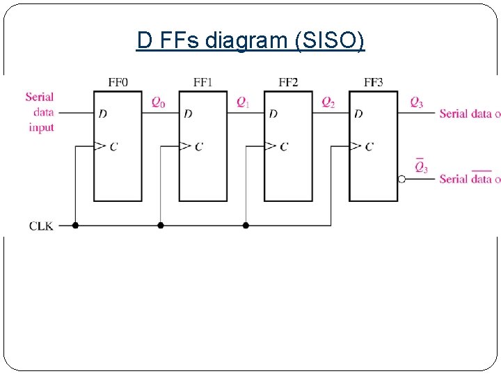
D FFs diagram (SISO)
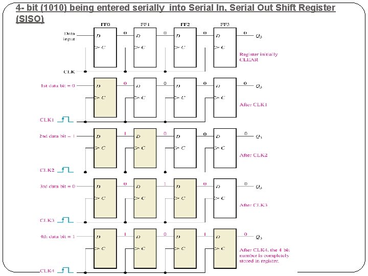
4 - bit (1010) being entered serially into Serial In, Serial Out Shift Register (SISO)
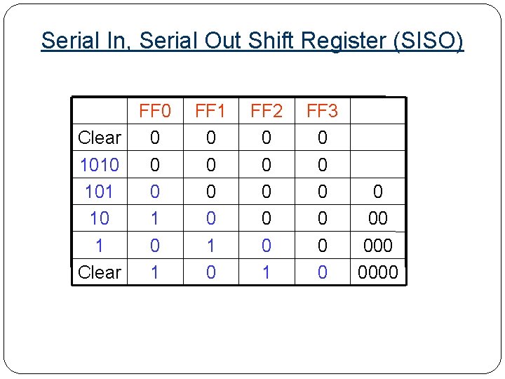
Serial In, Serial Out Shift Register (SISO) FF 0 Clear 0 1010 0 101 0 10 1 1 0 Clear 1 FF 1 0 0 1 0 FF 2 0 0 0 1 FF 3 0 0 0 00 0000
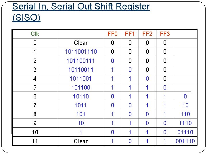
Serial In, Serial Out Shift Register (SISO) Clk FF 0 FF 1 FF 2 FF 3 0 Clear 0 0 1 1011001110 0 0 2 101100111 0 0 3 10110011 1 0 0 0 4 1011001 1 1 0 0 5 101100 1 1 1 0 6 10110 0 1 1 1 0 7 1011 0 0 1 1 10 8 101 1 0 0 1 110 9 10 1 1 0 0 1110 10 1 1 0 01110 11 Clear 1 0 1 1 001110
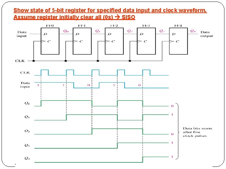
Show state of 5 -bit register for specified data input and clock waveform. Assume register initially clear all (0 s) SISO
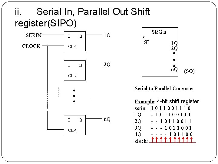
ii. Serial In, Parallel Out Shift register(SIPO) SERIN CLOCK D Q 1 Q CLK D Q 2 Q CLK 1 Q 2 Q n. Q (SO) Serial to Parallel Converter D > SI SRG n Q n. Q Example: 4 -bit shift register serin: 1 0 1 1 0 0 1 1 1 0 1 Q: - 101100111 2 Q: - - 10110011 3 Q: - - - 1011001 4 Q: - - 101100 clock:
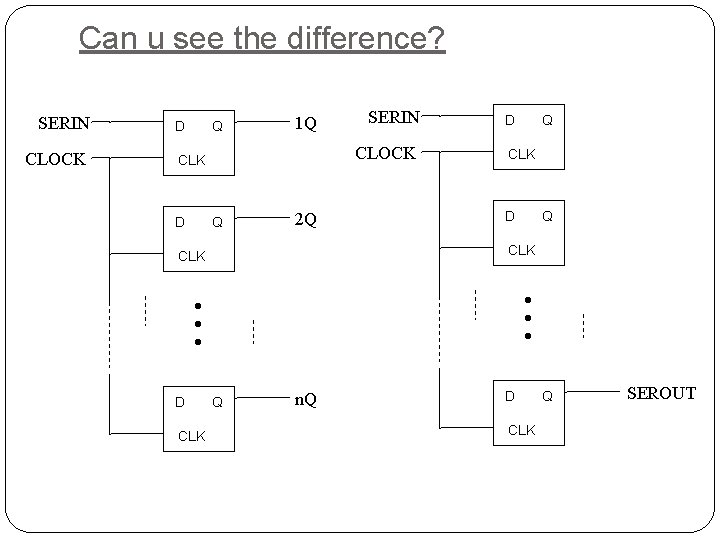
Can u see the difference? SERIN CLOCK D Q 1 Q CLOCK CLK D SERIN Q 2 Q D Q CLK CLK D CLK Q n. Q D CLK Q SEROUT
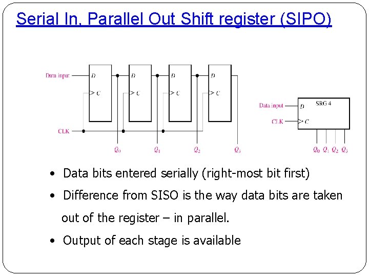
Serial In, Parallel Out Shift register (SIPO) • Data bits entered serially (right-most bit first) • Difference from SISO is the way data bits are taken out of the register – in parallel. • Output of each stage is available
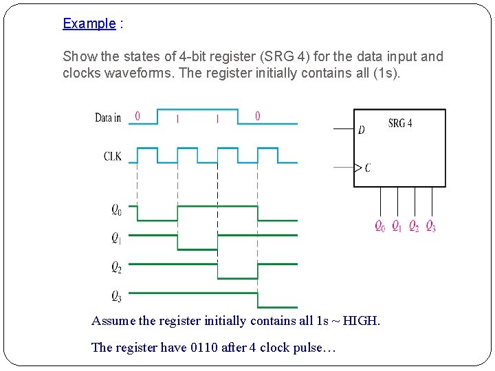
Example : Show the states of 4 -bit register (SRG 4) for the data input and clocks waveforms. The register initially contains all (1 s). Assume the register initially contains all 1 s ~ HIGH. The register have 0110 after 4 clock pulse…
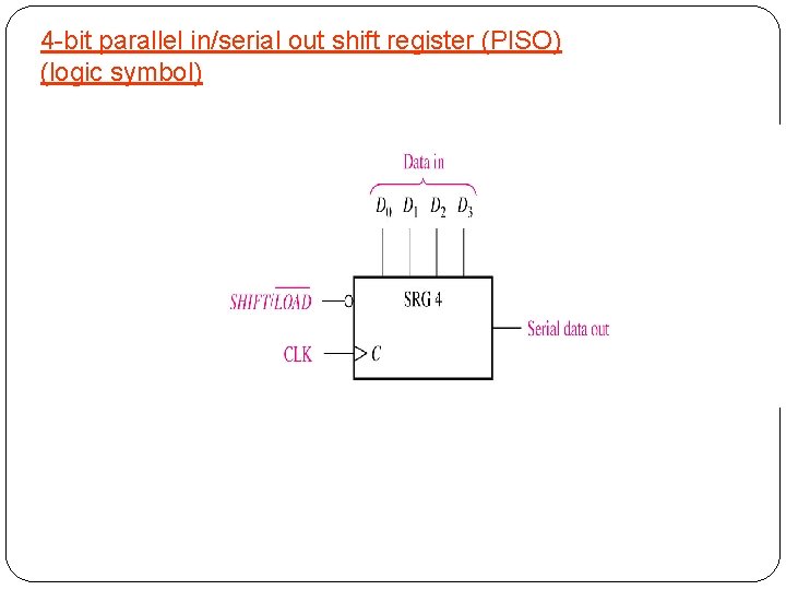
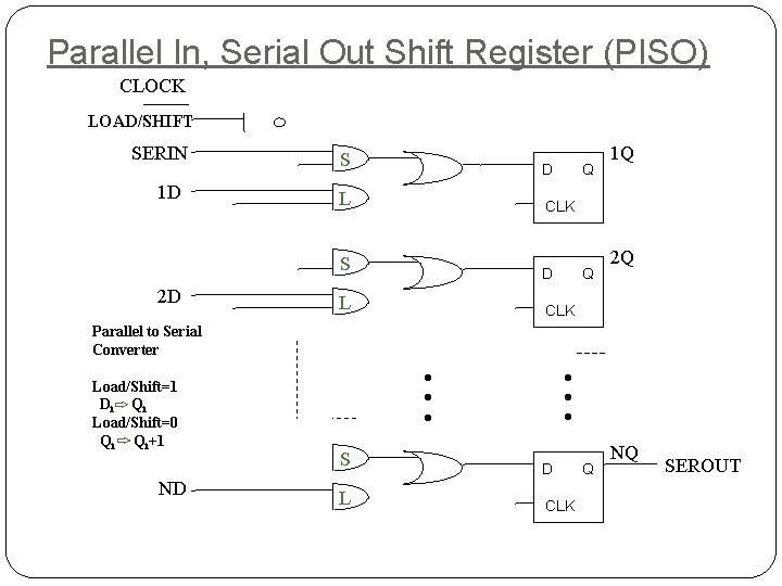
4 -bit parallel in/serial out shift register (PISO) (logic symbol)
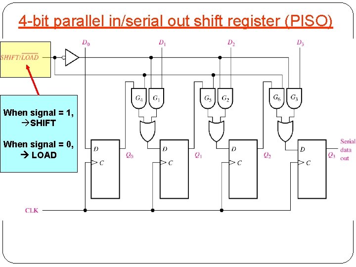
4 -bit parallel in/serial out shift register (PISO) When signal = 1, SHIFT When signal = 0, LOAD
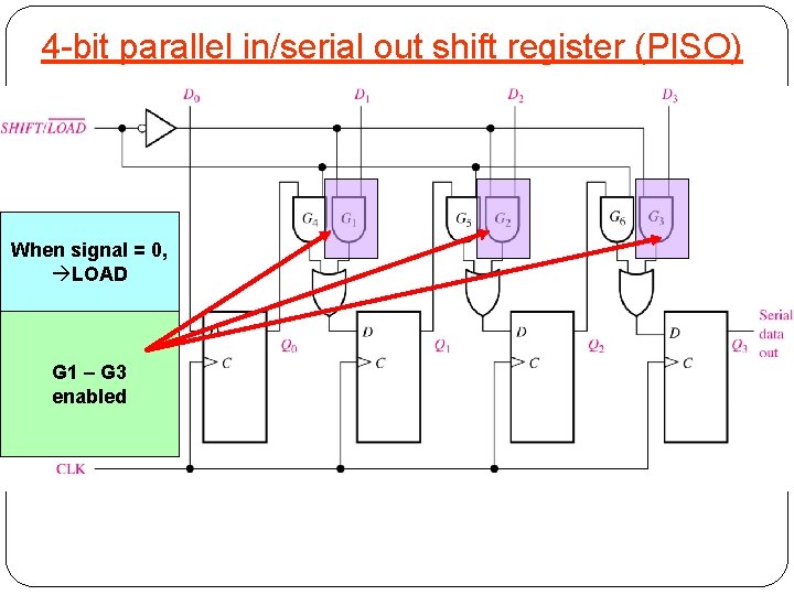
4 -bit parallel in/serial out shift register (PISO) When signal = 0, LOAD G 1 – G 3 enabled
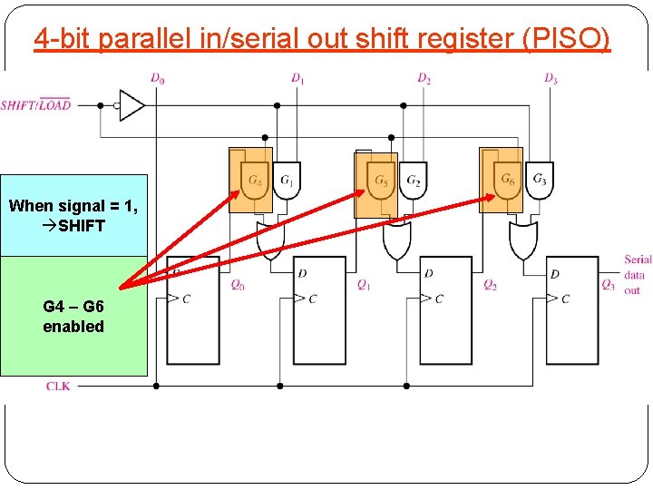
4 -bit parallel in/serial out shift register (PISO) When signal = 1, SHIFT G 4 – G 6 enabled
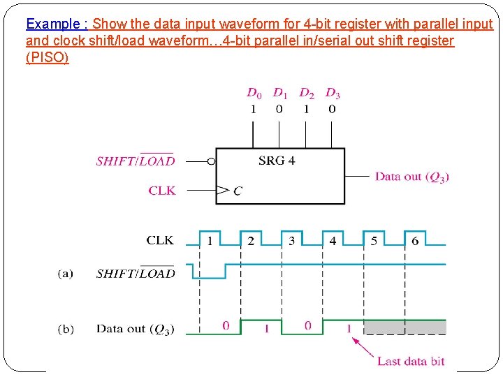
Example : Show the data input waveform for 4 -bit register with parallel input and clock shift/load waveform… 4 -bit parallel in/serial out shift register (PISO)
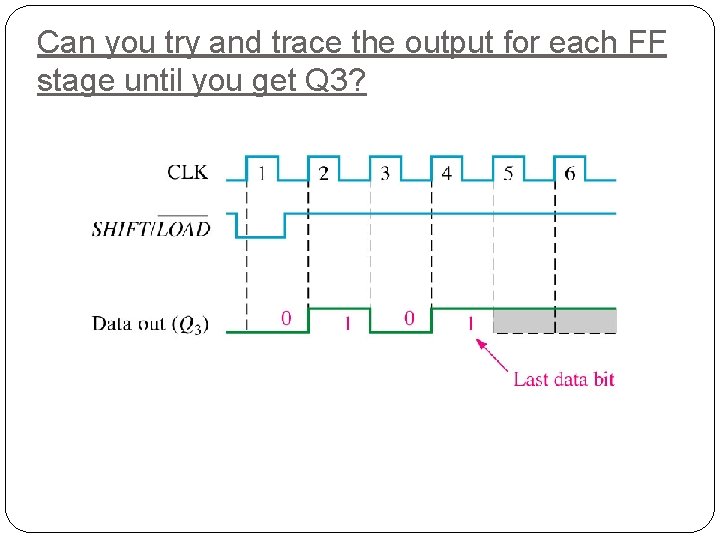
Can you try and trace the output for each FF stage until you get Q 3?

Let’s try to trace this one first… 1 0 1 Assume that the signal has values 011011 for 6 respective clock cycle For the parallel data input Assume D 0 = 1, D 1 = 0, D 2 = 1, D 3 = 0 0
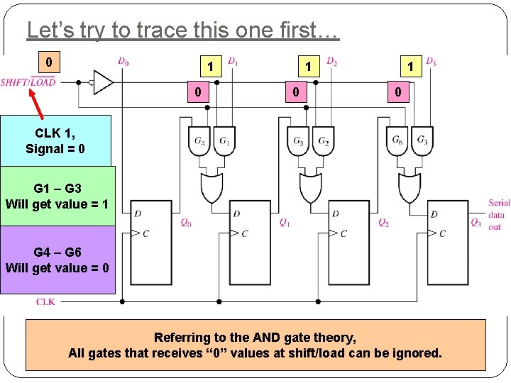
Let’s try to trace this one first… 0 1 0 1 0 CLK 1, Signal = 0 G 1 – G 3 Will get value = 1 G 4 – G 6 Will get value = 0 Referring to the AND gate theory, All gates that receives “ 0” values at shift/load can be ignored.
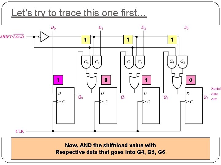
Let’s try to trace this one first… 1 1 1 0 1 1 Now, AND the shift/load value with Respective data that goes into G 4, G 5, G 6 0
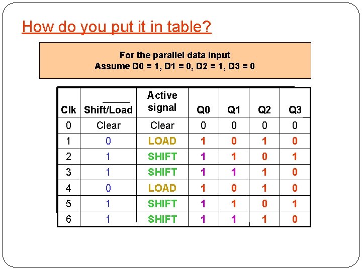
How do you put it in table? For the parallel data input Assume D 0 = 1, D 1 = 0, D 2 = 1, D 3 = 0 Clk Shift/Load Active signal Q 0 Q 1 Q 2 Q 3 0 Clear 0 0 1 0 LOAD 1 0 2 1 SHIFT 1 1 0 1 3 1 SHIFT 1 1 1 0 4 0 LOAD 1 0 5 1 SHIFT 1 1 0 1 6 1 SHIFT 1 1 1 0
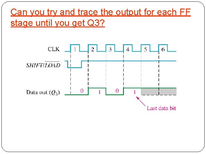
Can you try and trace the output for each FF stage until you get Q 3?
Parallel In, Serial Out Shift Register (PISO) CLOCK LOAD/SHIFT SERIN 1 D S D L CLK S 2 D Q 1 Q D L Q 2 Q CLK Parallel to Serial Converter Load/Shift=1 Di Q i Load/Shift=0 Qi Qi+1 ND S L D CLK Q NQ SEROUT
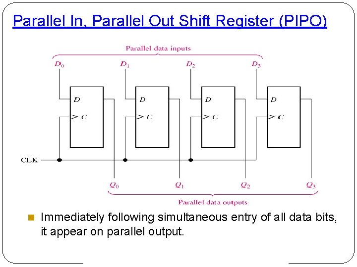
Parallel In, Parallel Out Shift Register (PIPO) Immediately following simultaneous entry of all data bits, it appear on parallel output.
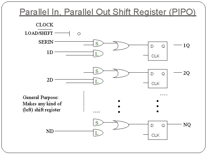
Parallel In, Parallel Out Shift Register (PIPO) CLOCK LOAD/SHIFT SERIN S 1 D L Q 2 Q Q NQ CLK S ND D L General Purpose: Makes any kind of (left) shift register 1 Q CLK S 2 D Q D CLK
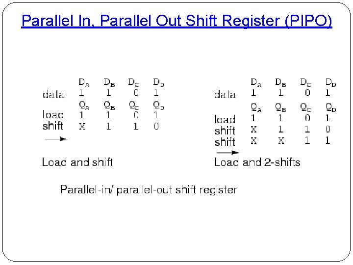
Parallel In, Parallel Out Shift Register (PIPO)
Bi-directional Shift Registers Data can be shifted left/right A parallel load maybe possible 74 HC 194 is a bidirectional universal shift register A bidirectional Shift Register ~ - one is which data can be shifted either left or right. - can be implement by using gate logics that enable transfer data bit from one stage to next stage (to right/left) depend on level of control lines.
Shift Registers Counter Shift register counter is basically a shift register with serial output connect back to serial input to produce sequences. Have 2 types : - (i) Johnson Counter = complement of output of last FF is connected back to D input of 1 st FF. (ii) Ring Counter = utilize one FF for each state in it sequence.
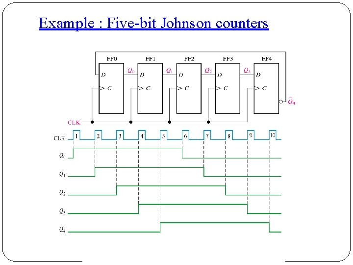
Example : Five-bit Johnson counters
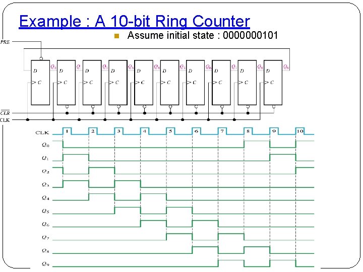
Example : A 10 -bit Ring Counter Assume initial state : 0000000101
Shift Register Applications Bit Serial Operations Bit serial operations can be performed quickly through device iteration Iteration (a purely combinational approach) is expensive (in terms of # of transistors, chip area, power, etc). A sequential approach allows the reuse of combinational functional units throughout the multi-cycle operation
Time Delay Time delay can be adjust up/down by changing the clock frequency Time delay can be increased by cascading shift register Time delay also can be decreased by taking output from lower stage
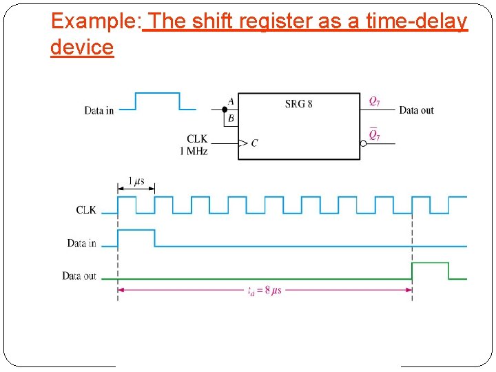
Example: The shift register as a time-delay device
Serial to parallel Conversion Use to reduce number of wires in transmission line. e. g. : eight bits can sent serially over one wire, but it takes 8 wires to send same data in parallel In the operation of serial to parallel converter: - consists of 11 bits(start bit=always 0 and always begin HIGH to LOW transition, 8 bits(D 7 -D 0)=data bit(1 parity bit, 2 stop bits) HIGH to LOW transition set the control flip-flop, enable the clock
- Slides: 41